The focusing effect of electron flow and negative refraction in three-dimensional topological insulators
Abstract
We studied the focusing effect of electron flow induced by a single p-n junction (PNJ) in three-dimensional topological insulator. It is found that the electrons flowing from the n region can be focused at the symmetric position in the p region, acting as a perfect Veselago lens, regardless whether the incident energy is within or beyond the bulk energy gap. In the former case, the focusing effect occurs only in the surfaces. While in the latter case, the focusing effect occurs beyond the surfaces. These results show that the focusing effect of electron flow is a general phenomenon. It means the negative refraction may arise in all materials that are described by the massive or massless Dirac equation of 2D or beyond 2D system. Furthermore, we also find the focusing effect is robust in resisting the moderate random disorders. Finally, in the presence of a weak perpendicular magnetic field , the focusing effect remains well except that the position of the focal point is deflected by the transverse Lorentz force. Due to the finite size effect, the position of focal point oscillates periodically with a period of .
pacs:
73.23.-b 73.43.-f 73.40.Gk, 72.20.-iI INTRODUCTION
In 1960s, Veselago theoretically predicted the existence of negative refractive index material, i.e., left-handed material.Veselago (168); Ward et al. (2005) After about 30 years, the first artificial left-handed material was experimentally verified.Shelby (2001) In general, electromagnetic negative refraction can only be realized in artificial constructed metamaterials because of the negative and ,Smith (2004) where and are the electric permittivity and the magnetic permeability, respectively. However, concerning the wave vector and group velocity, the optical rays and the electron flow (electron’s de Broglie wave) are similar, so the negative refraction would be achieved in real massless Dirac fermion materials, such as graphene. In a real material, the negative refraction is directly related to perfect Veselago lensPendry (2000) and Klein paradox.Guney and Meyer (2009)
The existence of negative refraction in massless Dirac material is natural. The electrons and holes in massless Dirac material are conjugately linked and interconnected, the chiralities (or dispersions) in conductance band and valence band are opposite. Then, the potential barrier induced by p-n junction (PNJ) is highly transparent for the charge carriers,Katsnelson et al. (2006) As a result, the electron flow would be negatively refracted and symmetrically focused by the straight interface of PNJ in the linear dispersion region.Cheianov et al. (2007) Beyond the linear region, the statement on Dirac fermion fall through, however, the focusing effect exists still.Xing et al. (2010) It means the negative refraction is not limited to the two dimensional massless Dirac materials. In fact, as shown in Fig.1, when electrons with momentum and velocity penetrate through PNJ and become holes with momentum , due to the opposite dispersion for electrons and holes, the velocity of holes becomes , then the negative refraction is formed. As a result, the electron flow is focused by the straight interface induced by PNJ. Here, ’’ denotes the direction along for two dimensional system or - plane for three dimensional system. So, there are two essential conditions to the focusing effect of electron flow. One is the opposite dispersions in conductance band and valence band, the other is the nearly transparent PNJ. In principle, besides massless Dirac FermionsFleury and Alu (2014); Pendry et al. (2012), all gapless semi-metal and topological materialsZhao et al. (2015); Sessi et al. (2016) described by quadratic massive Dirac equation in two dimension (2D) or beyond 2D, such as the 3D topological insulator (TI), ought to have the same effect. Considering the helical resolved characters of the TI materials, the focusing effect in TI can have great potential in the applications of helicity-based electron opticsZhao et al. (2015).
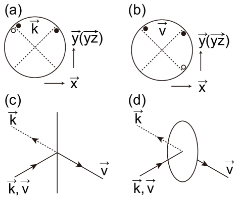
In the past years, due to the extraordinary band structure and huge potential in making future devices, TI have attracted great attentionsHasan and Kane (2010); Qi and Zhang (2011); Murakami (2003); Bernevig et al. (2006); König et al. (2007); Chen et al. (2009); Zhang et al. (2009); Yu et al. (2010); Chang et al. (2013); Zhang et al. (2010); Shan et al. (2010) in condensed matter physics. For a 3D TI such as ,Chen et al. (2009); Zhang et al. (2009) the electrons on conducting surface are massless Dirac Fermions depicted as a single Dirac cone. On the other hand, when the fermi energy is beyond the energy band gap, TI is similar as a conventional semiconductors because of the separated bands (conductance band and valence band). Then, what about the focusing effect of electron flow in 3D TI considering these different states of matter? can we find the focusing effect in deep conductance/valence band?
To answer these questions, we’ve constructed the PNJ in an infinite 3D TI ribbon as shown in Fig.2(a). With the aid of non-equilibrium Green’s function, we study the local conductance response to the non-equilibrium electron injection in 3D TI with single PNJ. It is found that when the incident energy is in the bulk gap, the transport processes are dominated by the surface states, and the focusing effect then arises only on the surfaces. As shown in Fig.2(a), on each side surface, electrons flow injected (the blue points) from n region (blue region) can be focused in the p region (red region) in the symmetric position (the red points). It is not strange since the surface states of 3DTI satisfy the 2D massless Dirac equation. When the incident energy is beyond the bulk energy gap, TI resembles the conventional semiconductors. However, because of the conjugated interconnection between the conductance band and valence band, the focusing effects in the bulk is even better. In this case, the electron flow incident from any site with the position of in the n region would be focused at position in the p region. Although supported by both surface and bulk states, the focusing effect can not be observed when these two type of states are mixed (near the energy band edges), because of the different dispersion for surface states and bulk states. Furthermore, we have also studied the influence of random scattering and the weak external magnetic field on the focusing effect. It is found that the focusing effect is immune to random disorders. In the presence of weak perpendicular magnetic field , the focus point is deviated by the lateral Lorentz force, however, the focusing effect retains well. Owing to the finite size of the scattering region, with the increasing , the position of the focus oscillates periodically with the period of , where is the area of central p region.
The paper is organized as follows. In Sec. II, from the low energy effective model, we present the system Hamiltonian in real space using tight binding technique. Then, both the partial local density and the local conductance describing the local response to the non-equilibrium source, i.e., the incident electron flow, are derived. Sec. III is the numerical results and some discussions. Finally, a summary of our work is presented in Sec. IV.
II MODEL AND FORMALISM
Through perturbation, the low energy effective Hamiltonian of 3D TI can be expanded in the Hilbert space composed with four low-lying states at point, i.e., , , and . Correspondingly, the Hamiltonian of infinite 3D TI is written in the following form: Zhang et al. (2009); Liu et al. (2010); Qi and Zhang (2011)
| (1) |
where, and represent the real spin ( and ) and pseudo-spin (signing the orbital and ) with . and are unitary matrix. , . Here, we set since it shifts the Dirac point and doesn’t change the topological structure of the Hamiltonian. To investigate the spacial focusing effect, the Hamiltonian expressed in real space is needed. Replacing by , we get 3D effective tight-binding Hamiltonian in a square lattice, as follows:Zhang et al. (2014a)
| (2) |
with
where, , denotes the four low-lying states at point, is the onsite energy at each lattice site. Here, is used to indicate the discrete sites of the square lattice with lattice constant . Considering the perpendicular magnetic field , the extra phase is inducedChen et al. (2012); Zhang et al. (2014b) by the magnetic vector potential . In the Coulomb gauge, the vector potential is set as and the magnetic flux at each lattice is then . For an infinite nanoribbon shown in Fig.2(a), and are finite and . The incident electrons are free in the -direction if PNJ is absent.
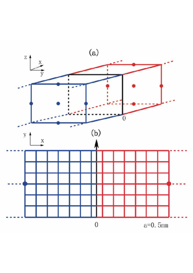
In the presence of the sharp PNJ that is induced by a step potential , the system is composed with semi-infinite electron-like n region (, the blue region in Fig.2(a) where ) and semi-infinite hole-like p region (, the red region in Fig.2(a) where ). Because the semi-infinite p region and n region are ideally periodical, the incident electrons can only scattered by the straight interface [the black interface in the Fig.2(a)], i.e., the sharp PNJ located at . Here, electrons are locally injected through source terminal and detected through drain terminal . The total Hamiltonian including the source and detection terminals is then expressed as
| (3) |
with
where denotes the infinite nanoribbon with sharp PNJ. denotes the source or detecting terminal used to inject or detect electron flow. Phenomenologically, is expressed in the momentum space. is the coupling between the source or detection electrode and the infinite ribbon. Here, we assume the electron flow is locally injected at the site in the n region and detected at site in the p region. For convenience, we define the central scattering region [the solid box in Fig.2(a)] enclosing the injecting site and detecting site. Concerning the central scattering Hamiltonian , the total Hamiltonian can also be written in the following form:
| (4) |
Eq.(4) describes a typical open system. Here, we can treat as open boundaries, denoting the source electrode, the detection electrode and the left and right semi-infinite lead, respectively. is the coupling between central scattering region and open boundaries. Obviously, , and
| (5) |
Next, with the help of the NEGF, the response signals, i.e., the local density in the scattering region are calculated as follows.
| (6) |
where is the diagonal element of the lesser Green’s function. Using Keldysh equation Jauho et al. (1994), the lesser Green’s function can be written as
| (7) |
Here, and are retarded and advanced Green’s function of the scattering region, respectively. , is the Fermi distribution function of the terminal-. In the nonequilibrium system, the Fermi energy of the terminal- is shifted by the external bias , and , where is the fermi distribution function with zero bias. The linewidth function with being the retarded self energy induced by the lead-. For the left and right seimi-infinite lead, , where is the coupling from the central region to the left or right lead, is the surface Green’s function of the semi-infinite lead, which can be calculated iteratively using transfer matrixM. P. Lopez Sancho and Rubio (1984, 1985) or Bloch eigenvector.Lee and Joannopoulos (1981a, b) The source and detection terminal are expressed in the momentum space. In the wide band limit, the self energy of the source or the detecting lead is . Comparing with injecting terminal, the influence of the detection terminal is much weaker, i.e. . In this case, we can neglect , then with .
In our calculation, the electron flow is injected from source terminal, the left and right semi-infinite lead are all the drain terminals. So, we set and . Finally, the lesser Green’s function can be divided into equilibrium and nonequlibrium term, i.e., with
| (8) |
Here, only the nonequlibrium term contributes to the response signals. It means
In zero temperature and linear bias limit, . Then, we can define the local partial density
| (9) |
On the other hand, we can also calculate the local conductance, which is defined as , where is the current flowing to the detection terminal that is located at site . According to the Landauer-Büttiker formalism,
Since we have set , the local conductance is then expressed as
| (10) |
Here, is a constant, so the local conductance is equivalent to the partial density, i.e., . In the following numerical calculation, only the local partial density is considered.
III NUMERICAL RESULTS AND DISCUSSION
In the numerical calculation, the parameters of 3DTI are set as ,Liu et al. (2010) , , , , ,Zhang et al. (2009) the lattice constant . Here we set , so the (kinetic) energy (relative to the energy of point) of electrons and holes are and , respectively.
III.1 Focusing effect in the linear regime
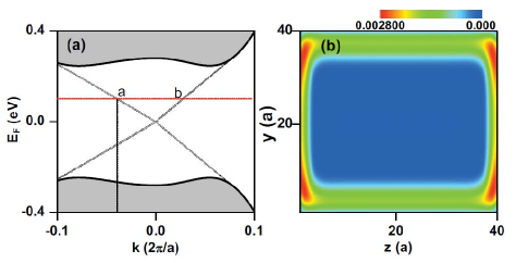
For the 3D TI, because of the band inversion near point, the nontrivial energy gap is induced. When is small, the energy gap is roughly determined by . In our model, the global bulk energy gap is about in the interval of [-0.245eV,0.245eV]. When the incident energy of electron is within the bulk energy gap, all the bulk states are forbidden, only the linear massless Dirac Fermions on the surfaces are permitted. In Fig.3, we first study the equilibrium density of state in this energy regime. According to fluctuation-dissipation theorem, , where is the surface Green’s function of semi-infinite 3D TI for fixed Fermi energy. In Fig.3(a) we plot the distribution of of infinite surface along - plan. The infinite surface is denoted by 2D momentum . In order to show the result intuitively, the momentum is set along the line of () and (), where , and are all the high symmetry points in momentum space. From Fig.3(a), we can clearly see the linear dispersion of the massless Dirac cone within the bulk energy gap that is bordered by the thick black lines in Fig.3(a). Fixing , the corresponding momentum along the path of is determined [the black dotted line in Fig.3(a)]. With this and , the local density of state in the finite cross section () of infinite ribbon is plotted in Fig.3(b). From Fig.3(b), we can clearly see the boundary states (the red region along the boundary) in the - section, depicting the surface states in the infinite ribbon.
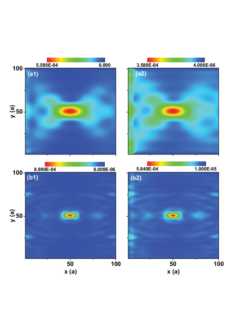
From Fig.3, we have confirmed the surface states in both momentum space and real space when the incident energy is within the bulk energy gap. In the following, we will study the focusing effect induced by these surface states. In Fig.4, we focus on the focusing effect in surfaces of 3D TI nanoribbon with straight PNJ potential within bulk energy gap. In Fig.4(a) and Fig.4(b), we plot the distribution of local partial density at the bottom layer in the p region () for and , respectively. The results in other surfaces are similar (not shown). The width and height of ribbon are set as , , respectively. The local partial density on bottom surface is the sum of the two layers at the lowest bottom, i.e., the layers at and . In the panel (a), electron flow is injected from the position in the n region, and focused at the position in the p region. While in the panel (b), the electron flow is injected from and focused at . It can be seen as long as the energy is within the energy gap, the electron flow can be perfectly focused at the symmetric position in the p region, no matter where it is injected in the n region, as analysed in the Fig.1. It is similar as in grapheneCheianov et al. (2007); Xing et al. (2010). Besides, we also find that the focusing effect for the higher energy () is better, which is totally different from the focusing effect in graphene, for which the focusing effect is worse for the higher energyXing et al. (2010). In addition, due to the extra scattering induced by the boundaries of the nanoribbon, there are regular interference patterns when the scattering region is long, as shown in the Fig.4(b).
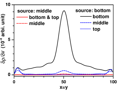
In the linear regime, the focusing effect is dominated by the surface states, so the focusing effect can’t happen in the deep of bulk. In Fig.5, considering a nanoribbon with size and , the distribution of local particle density along the diagonal line of the p region, i.e., , is plotted. Assuming the electron flow is injected from the middle layer (, red lines) and bottom layer (, black and blue lines), we plot at bottom, middle and top layers in the p region. Here, of the middle layers is the sum of the five middle layers, i.e., the layers located at =4.5-8.5. of the bottom (top) layers is the sum of the four lowest (highest) layers, i.e., the layers located at =0.5-3.5 (9.5-12.5). It is found when injecting electron flow from middle layer, the local response in the p region is uniformly small in all layers, which means no focusing effect happens when electron source is located deep inside the bulk. On the other hand, when injecting electron flow from the bottom layer, increases abruptly in the center of the bottom layers (see the black line in Fig.5), and becomes very small in the middle and top layers (the blue lines). In a word, in the low energy linear regime, the focusing effect of electron flow is dominated by the surface states and arises only in the surfaces of 3D TI ribbon.
III.2 Focusing effect in high energy regime
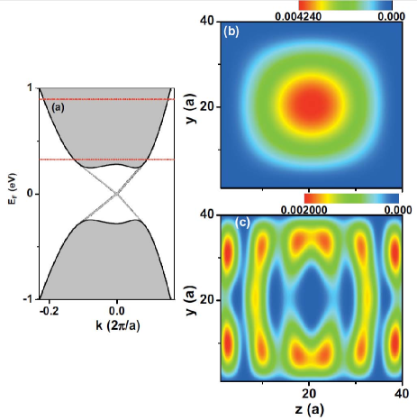
When the incoming Fermi energy is beyond the bulk energy gap, carriers are no longer described by linear Dirac cone. How about the focusing effect in this case? In Fig.6(a), we show the distribution of equilibrium density of state in whole energy regime for an infinite surface of a semi-infinite 3D TI. Both the discrete surface states (gray lines) and continuous bulk states (gray region bordered by black band edges) appear in Fig.6(a). Two cases are considered: Fermi energy is near band edge () and deep in conductance band () [see the red dotted lines in Fig.6(a)]. With these , the local density of state in the finite cross section () of infinite ribbon is plotted in Fig.6(b) and Fig.6(c). We can see near the band edge [eV, panel (b)] the surface states of the infinite ribbon are disturbed meanwhile the bulk states have not yet predominated. When is deep in conductance band [eV, panel (c)], the surface states disappear completely. Then, the system is dominated by the bulk states that do not obey the massless linear Dirac equation. In the following we will study the focusing effect induced by the bulk states.
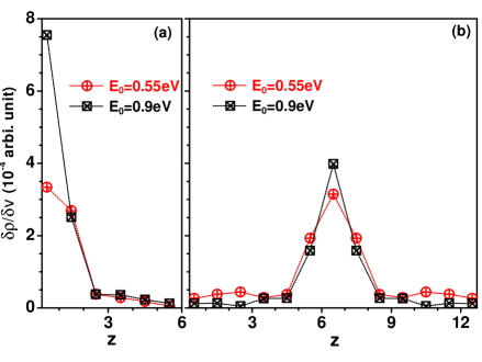
We first set PNJ potential . In this case, the bulk states dominate the transport processes. As a result, the focusing effect can occur in bulk as well as the surfaces, which is different from the focusing effect in the linear energy regime. Injecting electron flow from the bottom layer located at , we plot the local partial density in the center of p region at every layer signed by its coordinate in Fig.7(a). The height of the nanoribbion is . It can be seen becomes maximum at bottom - plane with since electron source is located in bottom layer. When deviating from the bottom layer, reduces abruptly to nearly zero. Next, we set and inject electron flow from the middle layer (). in the center of p region at every layer is plotted in the Fig.7(b). We can see becomes maximum at the middle bulk layer () and decreases abruptly at other layers. In other words, wherever injected from the n region, the electron flow can always be perfectly focused to the site in the p region. It means except the 2D linear massless Dirac Fermions, the conventional semi-metal can also produce the focusing effect.
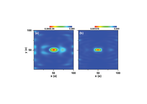
In general, it is difficult to embed the source lead deep into the bulk. So, in the following, the source terminal is assumed to be located in the bottom surface. Of course, the focusing effect occurs on the bottom surface as well. However, we must keep in mind that this focusing is dominated by bulk states, not by surface states. In Fig.8, we plot the distribution of local partial density in the p region for and that are all deep inside the bulk energy band. Here, the local partial density in the bottom surface is the sum of the two lowest layers ( and ). From Fig.8, we can see the perfect focusing effect in the high energy regime. The higher the PNJ potential, the better the focusing effect is. Different from the Fig.4, this focusing effect is induced by the conventional bulk states with quasi-quadratic dispersion.
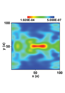
Up to now, we have shown that both the surface states (with linear dispersion) and the bulk states (with quadratic dispersion) can produce focusing effect. Now, we wonder if the focusing effect is going to happen when the surface states and the bulk states are mixed. In Fig.9, we plot the distribution of local partial density in p region for . When , the Fermi energy is near band edge, surface sates and bulk states coexist as shown in Fig.6(b). From Fig.9, we can see the focusing effect induced by the mixed states is really much worse compared to the Fig.4 or Fig.8 in which the pure surface states or bulk states are dominant. It is not strange because the dispersion of surface states and the bulk states are different, the mixture states can’t synchronously penetrate PNJ through the Klein tunnelingCheianov et al. (2007). The poor focusing in Fig.9 just reveals the different behaviors between the surface states and bulk states.
III.3 Influence of disorder on focusing effect
In the real device, disorder is inevitable. In this subsection, we will study the influence of disorder. In general, the impurities may appear near the interface due to the preparation of the PNJ. Disorders induce random scattering which is simulated by the random on-site potentialXing et al. (2011); Chen et al. (2012) uniformly distributed in the interval [], where is the disorder strength. Due to the disorder, the on-site energy now becomes . In the numerical calculation, disorders are distributed near the PNJ in the region from to . The numerical results are averaged over 200 random configurations.
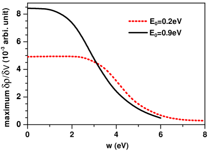
In Fig.10 and Fig.11, we study the focusing effect in the presence of random disorder. Both the surface states dominated focusing effect () and bulk states dominated focusing effect () are studied. In Fig.10(a) and Fig.10(b), we plot the distribution of local partial density for and , respectively. The disorder strength is set as that is very strong comparing to the PNJ potential . From Fig.10, we can see in the presence of strong disorders focusing effects dominated by both the surface states and the bulk states survive successfully. Comparing Fig.10(b) with Fig.8(b), it can be found in the presence of strong disorders the patterns of distribution are hardly affected. So, the focusing effect is quite immune to random disorders, no matter it is dominated by surface states or bulk states. It means the robust focusing effect is a general phenomena, not limited to the massless Dirac Fermions. It is promising for the future device designs.
Comparing Fig.8(b) and Fig.10(b), we can see that although the focusing patterns are kept well, the focusing intensity, i.e., the maximum , is reduced severely in the presence of strong disorder. In Fig.11, we plot the maximum value of local partial density vs random disorder strength . Here the maximum value is the sum of local partial density of the nine sites around the central focus (located at). From Fig.11, we can find for the bulk states dominated focusing (), the intensity is maintained when . When the disorder is strong enough to destroy the PNJ, the maximum decreases rapidly, until the focusing patterns are finally smeared. Correspondingly, the focusing effect induced by the PNJ is out of work. For the surface states dominated focusing (), the maximum remain unchanged even in very strong disorder () because of the topological nature of the surface states. The focusing effect is kept until the disorder is strong enough to destroy the topological surface states. In summary, surface states dominated focusing effect is coarse but more robust than bulk states dominated focusing effect. In other words, the bulk states dominated focusing effect is finer but frangible comparing to surface states dominated focusing effect.
III.4 Effect of magnetic field on focusing
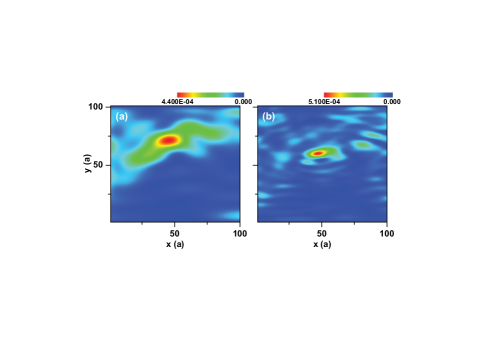
Besides the random disorders, the focusing effect is disturbed by external magnetic field. In the following, we will study the influence of the perpendicular magnetic field . In Fig.12(a) and Fig.12(b), we plot the distribution of local partial density for and , respectively. The magnetic field is set as . It can be seen the focusing pattern is disturbed and the focus point deviates from the central position of p region. Furthermore, comparing Fig.12(b) and Fig.8(b), we can see the focusing intensity is also reduced by . This is because the magnetic vector potential produces additional transverse velocity that breaks the conservation of momentum . As a result, the symmetric focusing process as analysed in the Fig.1 falls down, the focusing intensity is then weakened. Although weakened by the magnetic field , the focusing effect still exist in the p region. From Fig.12, we can clearly seen the deflected focus point.
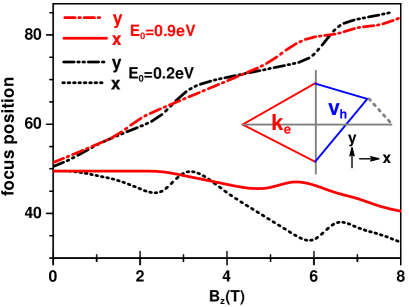
Let’s analyse how does the magnetic field affect the focusing effect. In the presence of magnetic field , the concomitant vector potential induces anomalous transverse velocity .Xiao et al. (2010) In our model, is positive (negative) for electrons (holes). Assuming the electrons are injected in the middle of the ribbon, the momentum is symmetrically distributed, the velocity of holes is shifted by positive as shown the inset of Fig.13. Then we can expect that the focus point (the blue point) is deflected. It deviates from the center of p region with negative and positive (gray dotted line in the inset of Fig.13). To track the deflection of focus point in the presence of magnetic field, we plot and coordinate of the focus position vs in the main panel of Fig.13. It can be seen with the increasing focus point deviates from the central point () of p region. It is true no matter the focusing effect is dominated by surface states () or bulk states (). The deflections of focus point are roughly the same for and . Besides, considering that the the central scattering region is finite, due to the finite size effect the track of the deflection of focus point oscillates periodically with the oscillating period of . This is because when the magnetic flux is quantized by ( is Planck constant and is electron charge), anomalous transverse velocity becomes maximum and or is correspondingly maximum. Furthermore, the oscillation is more violent for lower because the subbands are more discrete.
IV CONCLUSION
In summary, based on tight binding effective Hamiltonian and non-equilibrium Green’s function technique, the focusing effect of electron flow in 3D TI with single PNJ is studied. It is found the electrons/holes flow injecting from n/p region can be perfectly focused at the symmetric position in the p/n region, regardless whether the incident energy is within or beyond the bulk energy gap. It means in a 3D TI, the focusing effect can be produced by both surface states and bulk states effectively. So, The focusing effect in a PNJ is a general phenomena, not limited in the massless linear Dirac cones. Although the focusing effect is absolutely supported by both surface and bulk states, it can not appear when above two type of states are mixed (near the band edges), because of the incompatible dispersion for surface states and bulk states. Furthermore, we also study the influence of random scattering and the weak external magnetic field on the focusing effect. It is found the focusing effect is immune to random disorders. Finally, in the presence of a weak perpendicular magnetic field , the focusing effect remains, except the focus point is deflected by the transverse Lorentz force. The discoveries are beneficial for us to get a better insight on the topological materials.
This work is supported by the grant of Trans-Century Training Programme Foundation for the Talents by the State Education Commission (No. NCET-13-0048), and the grant from National Natural Science Foundation of China
(No. 11674024 and No. 11574019).
References
- Veselago (168) V. G. Veselago, Sov. Phys. Usp. 10, 509 (168).
- Ward et al. (2005) D. W. Ward, K. A. Nelson, and K. J. Webb, New Journal of Physics 7, 213 (2005), ISSN 1367-2630, URL http://dx.doi.org/10.1088/1367-2630/7/1/213.
- Shelby (2001) R. A. Shelby, Science 292, 77 (2001), ISSN 1095-9203, URL http://dx.doi.org/10.1126/science.1058847.
- Smith (2004) D. R. Smith, Science 305, 788 (2004), ISSN 1095-9203, URL http://dx.doi.org/10.1126/science.1096796.
- Pendry (2000) J. B. Pendry, Phys.Rev.Lett. 85, 3966 (2000), ISSN 1079-7114, URL http://dx.doi.org/10.1103/PhysRevLett.85.3966.
- Guney and Meyer (2009) D. O. Guney and D. A. Meyer, Phys. Rev. A 79 (2009), ISSN 1094-1622, URL http://dx.doi.org/10.1103/PhysRevA.79.063834.
- Katsnelson et al. (2006) M. I. Katsnelson, K. S. Novoselov, and A. K. Geim, Nature Physics 2, 620 (2006), eprint cond-mat/0604323.
- Cheianov et al. (2007) V. V. Cheianov, V. Faĺko, and B. L. Altshuler, Science 315, 1252 (2007), eprint cond-mat/0703410.
- Xing et al. (2010) Y. Xing, J. Wang, and Q.-F. Sun, Phys. Rev. B 81, 165425 (2010), eprint 1011.2821.
- Fleury and Alu (2014) R. Fleury and A. Alu, Physical Review B 90, 035138 (2014), ISSN 1550-235X, URL http://dx.doi.org/10.1103/PhysRevB.90.035138.
- Pendry et al. (2012) C. G. Pendry, J. B.terfalvi, L. Oroszlany, C. J. Lambert, and J. Cserti, New Journal of Physics 14, 063028 (2012), ISSN 1367-2630, URL http://dx.doi.org/10.1088/1367-2630/14/6/063028.
- Zhao et al. (2015) L. Zhao, J. Wang, J. Liu, Y. Xu, B.-L. Gu, Q.-K. Xue, and W. Duan, Physical Review B 92, 041408 (2015), ISSN 1550-235X, URL http://dx.doi.org/10.1103/PhysRevB.92.041408.
- Sessi et al. (2016) P. Sessi, P. Ru?mann, T. Bathon, A. Barla, K. A. Kokh, O. E. Tereshchenko, K. Fauth, S. K. Mahatha, M. A. Valbuena, S. Godey, et al., Physical Review B 94, 075137 (2016), ISSN 2469-9969, URL http://dx.doi.org/10.1103/PhysRevB.94.075137.
- Hasan and Kane (2010) M. Z. Hasan and C. L. Kane, Rev. Mod. Phys. 82, 3045 (2010), ISSN 1539-0756, URL http://dx.doi.org/10.1103/RevModPhys.82.3045.
- Qi and Zhang (2011) X.-L. Qi and S.-C. Zhang, Reviews of Modern Physics 83, 1057 (2011), eprint 1008.2026.
- Murakami (2003) S. Murakami, Science 301, 1348 (2003), ISSN 1095-9203, URL http://dx.doi.org/10.1126/science.1087128.
- Bernevig et al. (2006) B. A. Bernevig, T. L. Hughes, and S.-C. Zhang, Science 314, 1757 (2006), eprint cond-mat/0611399.
- König et al. (2007) M. König, S. Wiedmann, C. Brüne, A. Roth, H. Buhmann, L. W. Molenkamp, X.-L. Qi, and S.-C. Zhang, Science 318, 766 (2007), eprint 0710.0582.
- Chen et al. (2009) Y. L. Chen, J. G. Analytis, J.-H. Chu, Z. K. Liu, S.-K. Mo, X. L. Qi, H. J. Zhang, D. H. Lu, X. Dai, Z. Fang, et al., Science 325, 178 (2009).
- Zhang et al. (2009) H. Zhang, C.-X. Liu, X.-L. Qi, X. Dai, Z. Fang, and S.-C. Zhang, Nature Physics 5, 438 (2009).
- Yu et al. (2010) R. Yu, W. Zhang, H.-J. Zhang, S.-C. Zhang, X. Dai, and Z. Fang, Science 329, 61 (2010), URL http://dx.doi.org/10.1126/science.1187485.
- Chang et al. (2013) C.-Z. Chang, J. Zhang, X. Feng, J. Shen, Z. Zhang, M. Guo, K. Li, Y. Ou, P. Wei, L.-L. Wang, et al., Science 340, 167 (2013), URL http://dx.doi.org/10.1126/science.1234414.
- Zhang et al. (2010) W. Zhang, R. Yu, H.-J. Zhang, X. Dai, and Z. Fang, New Journal of Physics 12, 065013 (2010), ISSN 1367-2630, URL http://dx.doi.org/10.1088/1367-2630/12/6/065013.
- Shan et al. (2010) W.-Y. Shan, H.-Z. Lu, and S.-Q. Shen, New Journal of Physics 12, 043048 (2010), ISSN 1367-2630, URL http://dx.doi.org/10.1088/1367-2630/12/4/043048.
- Liu et al. (2010) C.-X. Liu, X.-L. Qi, H.-J. Zhang, X. Dai, Z. Fang, and S.-C. Zhang, Phys. Rev. B 82, 045122 (2010), eprint 1005.1682.
- Zhang et al. (2014a) L. Zhang, J. Zhuang, Y. Xing, J. Li, J. Wang, and H. Guo, Phys. Rev. B 89, 245107 (2014a).
- Chen et al. (2012) J.-C. Chen, J. Wang, and Q.-F. Sun, Phys. Rev. B 85, 125401 (2012).
- Zhang et al. (2014b) S.-f. Zhang, H. Jiang, X. C. Xie, and Q.-f. Sun, Phys. Rev. B 89, 155419 (2014b).
- Jauho et al. (1994) A.-P. Jauho, N. S. Wingreen, and Y. Meir, Phys. Rev. B 50, 5528 (1994), eprint cond-mat/9404027.
- M. P. Lopez Sancho and Rubio (1984) J. M. L. S. M. P. Lopez Sancho and J. Rubio, J.Phys.F: Met.Phys. 14, 1205 (1984).
- M. P. Lopez Sancho and Rubio (1985) J. M. L. S. M. P. Lopez Sancho and J. Rubio, J.Phys.F: Met.Phys. 15, 851 (1985).
- Lee and Joannopoulos (1981a) D. H. Lee and J. D. Joannopoulos, Phys. Rev. B 23, 4988 (1981a).
- Lee and Joannopoulos (1981b) D. H. Lee and J. D. Joannopoulos, Phys. Rev. B 23, 4997 (1981b).
- Xing et al. (2011) Y. Xing, L. Zhang, and J. Wang, Physical Review B 84, 035110 (2011), ISSN 1550-235X, URL http://dx.doi.org/10.1103/PhysRevB.84.035110.
- Chen et al. (2012) L. Chen, Q. Liu, X. Lin, X. Zhang, and X. Jiang, New Journal of Physics 14, 043028 (2012), ISSN 1367-2630, URL http://dx.doi.org/10.1088/1367-2630/14/4/043028.
- Xiao et al. (2010) D. Xiao, M.-C. Chang, and Q. Niu, Rev. Mod. Phys. 82, 1959 (2010), ISSN 1539-0756, URL http://dx.doi.org/10.1103/RevModPhys.82.1959.