Hybridization of sub-gap states in one-dimensional
superconductor/semiconductor Coulomb islands
Abstract
We present measurements of one-dimensional superconductor-semiconductor Coulomb islands, fabricated by gate confinement of a two-dimensional InAs heterostructure with an epitaxial Al layer. When tuned via electrostatic side gates to regimes without sub-gap states, Coulomb blockade reveals Cooper-pair mediated transport. When sub-gap states are present, Coulomb peak positions and heights oscillate in a correlated way with magnetic field and gate voltage, as predicted theoretically, with (anti) crossings in (parallel) transverse magnetic field indicating Rashba-type spin-orbit coupling. Overall results are consistent with a picture of overlapping Majorana zero modes in finite wires.
The prediction that a topological superconductor might be realized by combining accessible and well understood materials Lutchyn et al. (2010); Oreg et al. (2010) prompted an intense experimental effort into superconductor-semiconductor (super-semi) hybrid systems. Open geometries, i.e., without charging energy, have been instrumental to demonstrate transport behavior consistent with Majorana zero modes (MZMs) Mourik et al. (2012); Deng et al. (2016); Nichele et al. (2017); Zhang et al. (2018). However, proposals to manipulate pairs of MZM and probe their expected non-Abelian exchange statistics have focused on closed geometries such as Coulomb islands Aasen et al. (2016). In a superconducting Coulomb island, the Coulomb blockade (CB) period is a probe of the lowest sub-gap state energy Tuominen et al. (1992); Lafarge et al. (1993), making it a viable tool to study MZMs. This geometry was investigated by Albrecht et al. Albrecht et al. (2016), who showed that, in short wires, modes are no longer fixed at zero energy as the magnetic field increases, but instead oscillate. Oscillations in the CB period might, however, also occur at level-crossings of states having no topological character. Numerical simulations suggested several situations in which level-crossings could take place Chiu et al. (2017): multiple sub-band occupancy; the presence of trivial Andreev bound states; or, simply, if the spin-orbit interaction (SOI) is negligible.
Here, we experimentally investigate two aspects of one-dimensional super-semi wires relevant to the topological phase transition: the hybridization of particle- and hole-like sub-gap states, and the spin structure of those hybridized states. The wire-shaped Coulomb islands are lithographically patterned using a two-dimensional electron gas (2DEG) of InAs with an epitaxial layer of Al Shabani et al. (2016). Previous work has shown discrete zero-energy modes can be induced in this heterostructure Suominen et al. (2017); Nichele et al. (2017). We first show that the system can be tuned to a two-electron () periodic CB, indicative of no sub-gap states below the charging energy . When discrete sub-gap states are present, CB peaks spacing oscillate with gate voltage magnetic fields applied in the plane of the 2DEG. We focus on in-plane fields applied parallel () or transverse () to the wire. Coulomb peak spacing oscillations correlate with oscillations in peak conductance, as predicted for extended sub-gap states in clean Majorana wires undergoing a crossover in the spectral weight of their electron- and hole-like components Hansen et al. (2018). Investigating CB spacing as a function of field orientation, we conclude sub-gap states are subject to a Rashba-like SOI, and we provide a lower bound for the Rashba parameter.
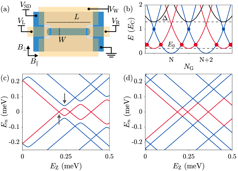
Figure 1(a) shows a schematic of the device, the measurement setup, and the field orientations used in this work. Following the approach of Ref. Suominen et al., 2017, an Al wire, with dimensions and , is etched into the epitaxial Al layer (blue) on top of the III-V heterostructure (gray), with the InAs quantum well 10 nm below the surface. Contact to the island is made via extended planes of the original Al epi-layer. Ti/Au gates (yellow) are deposited on an atomic layer depostion grown HfO2 dielectric. The voltage depletes the 2DEG surrounding the Al stripe, but not below it, and tunes the chemical potential of the resulting Coulomb island. Voltages and tune the transmission of the right and left tunneling barrier, respectively. We present results from two nominally identical devices (Device 1 and 2) with nm and nm, rotated with respect to each other, parallel to the and crystal directions, respectively. Data on an additional nm sample that did not show discrete sub-gap states, and did not demonstrate the correlation between CB spacing and conductance that is reported here, is shown in the Supplemental Material Sup , together with data from two longer islands that showed a decreased magnitude of sub-gap state oscillations consistent with Albrecht et al. (2016). Transport measurements were performed in a dilution refrigerator with a base temperature of via conventional lock-in techniques. A voltage bias was applied to one lead while the current and four-terminal voltage were recorded and used to calculate the differential conductance . Device 1 and Device 2 were aligned parallel and perpendicular, respectively, to the major axis of a vector magnet.
For a superconducting Coulomb island with negligible level spacing weakly tunnel coupled to metallic leads, the lowest energy state with charges is given by , where is the gate-induced occupancy, is the energy of the lowest unpaired quasiparticle state i.e. equal to the gap in the absence of sub-gap states, and is the charging energy [see Fig. 1(b)]. At zero bias, charge flows at degeneracy points , these are CB peaks. For transport occurs at blue squares in Fig. 1(b), the lowest energy state always has even occupation and pairs of electrons transfer into the dot condensate Tuominen et al. (1992); Hekking et al. (1993). However, when transport occurs in the odd state too [red dots in Fig. 1(b)], making CB spacing a probe for .
The combined effect of SOI and Zeeman field drives discrete bound states into the induced superconducting gap, ultimately leading to a topological phase transition and modes with for one-dimensional islands Oreg et al. (2010); Lutchyn et al. (2010). The calculated energy spectrum of the finite-length wires in the present experiment, versus Zeeman energy , is shown in Figs. 1(c) and (d) for magnetic field applied perpendicular and parallel to the direction of SOI, respectively. The model, described in Ref. Hell et al., 2017; Sup, , assumes a purely Rashba-like SOI where is the Rashba parameter, and are Pauli matrices for particle-hole and spin space, respectively, is the momentum and the -axis is defined to be parallel to the wire. That is, SOI lies in the plane of the 2DEG and perpendicular to the wire. As for conventional semiconductor nanostructures Bulaev and Loss (2005); Takahashi et al. (2010); Nichele et al. (2014), SOI mixes spin states, leading to the anti-crossing of iso-parity sub-gap states following the first zero-energy crossing of modes with opposite parity [up-pointing and down-pointing arrows in Fig. 1(c), respectively]. In contrast, when the external magnetic field is aligned to the spin-orbit field, spin-up and spin-down levels cross.
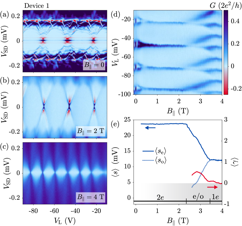
To investigate these spectral features experimentally, we tuned the sub-gap spectrum of the wire by adjusting the voltage on the side gate, which modifies both the chemical potential and the spatial confinement of electrons below the Al. The lowest sub-gap state energy was then probed by measuring the CB spacing while varying to change the island occupancy keeping the spectrum mostly unaltered Sup . Figure 2(a-c) show Coulomb diamonds versus at , and and for . At , enhanced conductance at , together with regular features at finite are attributed to a supercurrent and multiple Andreev reflection with the superconducting leads, respectively. At these features were absent and the spectrum was similar to that reported for superconducting devices with metallic leads Higginbotham et al. (2015). This observation is consistent with previous work on this heterostructure, showing that extended Al planes have a finite and smooth sub-gap density of states at , which is suitable for spectroscopy Suominen et al. (2017). At the system was normal and eV.
Figure 2(d) shows zero-bias conductance versus and . The spacing averaged over even (odd) valleys [Fig. 2(e)] was constant up to , indicating no sub-gap states, before decreasing linearly to half the zero-field value, when the normal state is reached. We refer to CB periodicities as , even/odd () and , respectively. Also shown is the normalized conductance ratio averaged over pairs of peaks. This quantity was found to become zero in the normal state. Its significance is discussed below in detail. Temperature dependence yields at T, and we estimated a parity lifetime ms Sup .
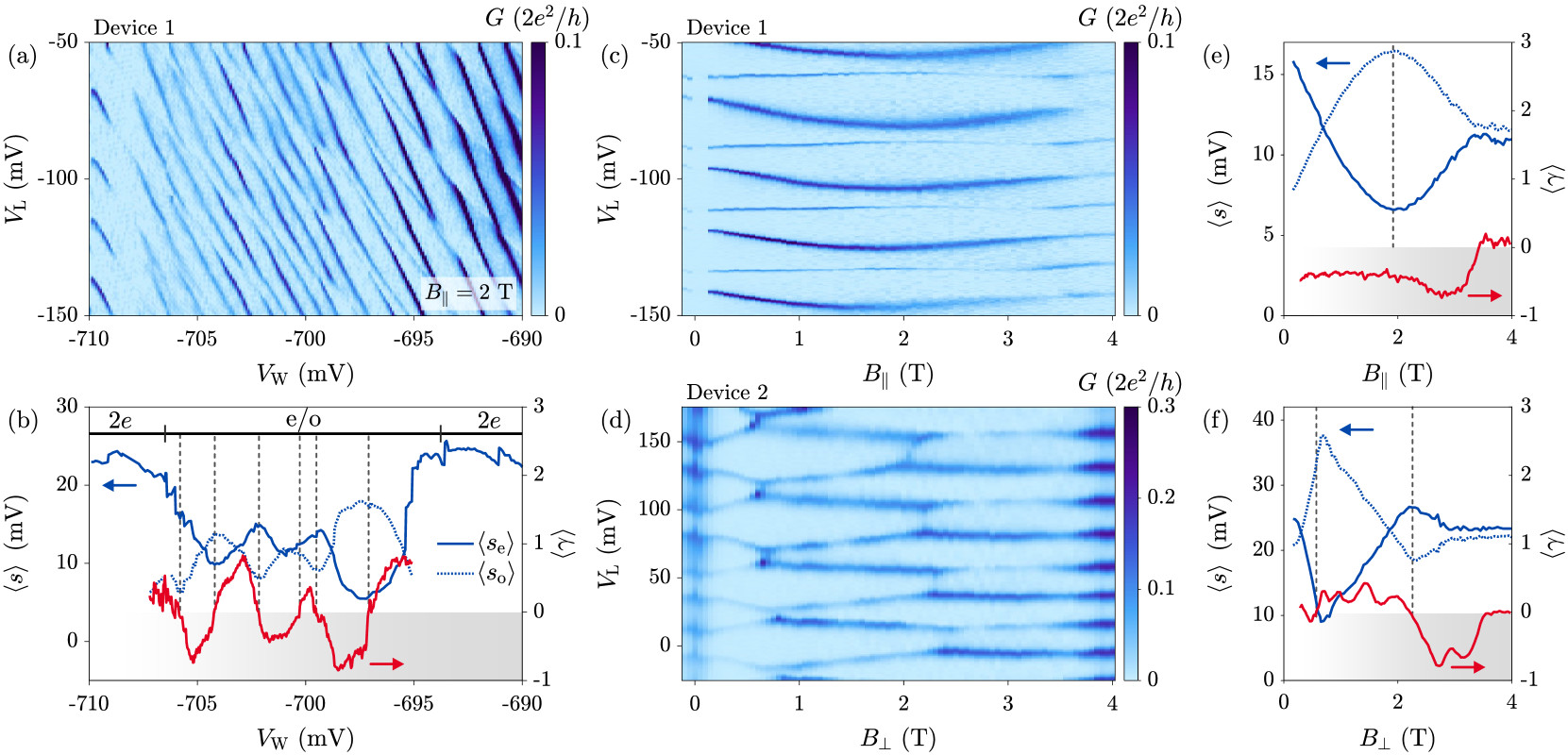
We next investigate the situation where discrete sub-gap states were present. Figure 3(a) shows the zero-bias conductance versus and at . We moved from the regime of Fig. 2, to more negative , periodic CB peaks were split, their spacing became even/odd and oscillated about a periodicity, indicating a sub-gap state energy . With a further reduction of , the state left the gap and charging was re-established. The average peak spacings versus are shown in Fig. 3(b) (left-axis), together with the average peak amplitude . Similar measurements as a function of gave compatible results Sup , with CB period almost independent of extended ranges of and , that indicated a state not localized to the ends of the wire. We also note that oscillations in were correlated with oscillations in : zero-crossings of matched extrema in . Figures 3(c) and (e) show the evolution in at . crossed zero energy at , and then oscillated with a maximum at . Figure 3(d) and (f) show the conductance ratio and peak spacing for a comparable regime in Device 2 under . In Fig. 3(f), zero-crossings of correlated with extrema in spacing. This becomes less evident in Fig. 3(e), presumably due to the small number of oscillations as a function of . In the Supplemental Material Sup we provide additional data on Device 2 and compare the oscillations in with direct tunneling spectroscopy of sub-gap states.
The observed relationship between and was predicted to be characteristic of oscillating sub-gap states in uniform nanowires Hansen et al. (2018); Sup . For a hybridized Majorana mode, oscillations in gate potential and magnetic field reflect oscillations in the electron-hole and spin components of the wavefunction, and vanish in the limit . The state of Fig. 3(a) is compatible with such an interpretation. Similarly, the oscillations seen in Fig. 3(d) for are consistent with a change in the lowest energy state, which dominates transport through the wire. Such a state is also expected to give rise to a Majorana mode for . Correlation between CB peaks spacing and amplitude, with a phase shift in their oscillations, was not previously reported and provides an additional tool for the identification of MZMs in Coulomb islands. In contrast, localized Andreev states Liu et al. (2017) are expected to show no particular relation between and Hansen et al. (2018).
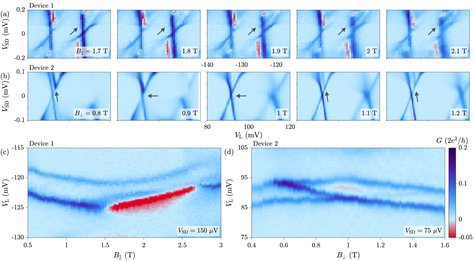
Oscillations of in or were qualitatively different: the smooth curvature in Fig. 3(d) contrasts with the sharp kinks in Fig. 3(f). This behavior reflects a different spin hybridization of sub-gap states for and . Figure 4(a) shows bias spectroscopy at several in the vicinity of the spacing maximum in Fig. 3(c). Negative differential conductance indicated blocking of quasiparticle tunneling into the state Hekking et al. (1993). This enabled us to estimate a quasiparticle tunneling rate, which, together with the quasiparticle density extracted from temperature dependence Sup and following the method of Higginbotham et al. (2015), provides an estimate of the parity lifetime of this state s at T. As increased, the excited state moved to lower energy; however, it did not reach the lowest energy state. Similarly, bias spectroscopy in for Device 2 [Fig. 4(b)] showed a discrete energy level was present for Device 2 in the vicinity of the first oscillation in Fig. 3(e). This showed the level became degenerate with the ground state energy at . The magnitude of negative differential conductance was strongly reduced for , that indicated a weakened blocking effect. Enhanced conduction within the valleys in Fig. 3(d), around maxima in the spacing, may be a signature of the orbital Kondo effect at degeneracy Sasaki et al. (2004).
To measure crossing and anti-crossing precisely, we fixed a finite and varied . Figures 4(c) and (d) show the results for and at and , respectively. For , the lowest energy state anti-crossed with an excited state and then moved back towards zero energy. The energy splitting averaged over the peaks of Fig. 3(c) was , corresponding to the mini-gap denoted by a down-pointing arrow in Fig. 1(c). Instead, for , the lowest energy and excited state exchanged position. The observation that parity states anti-cross for and cross for confirms that the dominant SOI in this system is of Rashba type. Further analysis Sup used the experimentally obtained anti-crossing energy [Fig. 4(c)] to estimate a lower bound of the Rashba parameter, meVÅ. This bound is compatible with the value extracted from anti-localization measurements ( meVÅ) of a similar heterostructure with all the Al removed Shabani et al. (2016).
In conclusion, InAs-Al 2DEG based hybrids are a suitable platform to fabricate clean super-semi Coulomb islands, with long parity lifetimes of bound states. Oscillations in energy of sub-gap states as a function of in-plane magnetic field and gate voltage are consistent with oscillations of parity bands of a Majorana mode. In the light of our results, devices of this kind offer great promise for MZM physics in multi-island geometries.
After completing this work we became aware of a related work by Shen et al. considering sub-gap states in InSb-Al super-semi nanowires Shen et al. .
Acknowledgements.
This work was supported by Microsoft Corporation, the Danish National Research Foundation, and the Villum Foundation. We thank J. Folk, J. Gamble, M. Leijnse, C. Olsen and H. Suominen for useful discussions.References
- Lutchyn et al. (2010) R. M. Lutchyn, J. D. Sau, and S. Das Sarma, Phys. Rev. Lett. 105, 077001 (2010).
- Oreg et al. (2010) Y. Oreg, G. Refael, and F. von Oppen, Phys. Rev. Lett. 105, 177002 (2010).
- Mourik et al. (2012) V. Mourik, K. Zuo, S. M. Frolov, S. Plissard, E. Bakkers, and L. P. Kouwenhoven, Science 336, 1003 (2012).
- Deng et al. (2016) M. Deng, S. Vaitiekėnas, E. B. Hansen, J. Danon, M. Leijnse, K. Flensberg, J. Nygård, P. Krogstrup, and C. M. Marcus, Science 354, 1557 (2016).
- Nichele et al. (2017) F. Nichele, A. C. C. Drachmann, A. M. Whiticar, E. C. T. O’Farrell, H. J. Suominen, A. Fornieri, T. Wang, G. C. Gardner, C. Thomas, A. T. Hatke, et al., Phys. Rev. Lett. 119, 136803 (2017).
- Zhang et al. (2018) H. Zhang, C.-X. Liu, S. Gazibegovic, D. Xu, J. A. Logan, G. Wang, N. van Loo, J. D. Bommer, M. W. de Moor, D. Car, et al., Nature 556, 74 (2018).
- Aasen et al. (2016) D. Aasen, M. Hell, R. V. Mishmash, A. Higginbotham, J. Danon, M. Leijnse, T. S. Jespersen, J. A. Folk, C. M. Marcus, K. Flensberg, et al., Phys. Rev. X 6, 031016 (2016).
- Tuominen et al. (1992) M. T. Tuominen, J. M. Hergenrother, T. S. Tighe, and M. Tinkham, Phys. Rev. Lett. 69, 1997 (1992).
- Lafarge et al. (1993) P. Lafarge, P. Joyez, D. Esteve, C. Urbina, and M. H. Devoret, Phys. Rev. Lett. 70, 994 (1993).
- Albrecht et al. (2016) S. M. Albrecht, A. Higginbotham, M. Madsen, F. Kuemmeth, T. S. Jespersen, J. Nygård, P. Krogstrup, and C. M. Marcus, Nature 531, 206 (2016).
- Chiu et al. (2017) C.-K. Chiu, J. D. Sau, and S. Das Sarma, Phys. Rev. B 96, 054504 (2017).
- Shabani et al. (2016) J. Shabani, M. Kjaergaard, H. Suominen, Y. Kim, F. Nichele, K. Pakrouski, T. Stankevic, R. M. Lutchyn, P. Krogstrup, R. Feidenhans, et al., Phys. Rev. B 93, 155402 (2016).
- Suominen et al. (2017) H. J. Suominen, M. Kjaergaard, A. R. Hamilton, J. Shabani, C. J. Palmstrøm, C. M. Marcus, and F. Nichele, Phys. Rev. Lett. 119, 176805 (2017).
- Hansen et al. (2018) E. B. Hansen, J. Danon, and K. Flensberg, Phys. Rev. B 97, 041411 (2018).
- (15) See Supplemental Material at [URL] for material and methods, and additional measurements, which include Ref. Shaw et al. (2008); Albrecht et al. (2017).
- Hekking et al. (1993) F. W. J. Hekking, L. I. Glazman, K. A. Matveev, and R. I. Shekhter, Phys. Rev. Lett. 70, 4138 (1993).
- Hell et al. (2017) M. Hell, K. Flensberg, and M. Leijnse, Phys. Rev. B 96, 035444 (2017).
- Bulaev and Loss (2005) D. V. Bulaev and D. Loss, Phys. Rev. B 71, 205324 (2005).
- Takahashi et al. (2010) S. Takahashi, R. S. Deacon, K. Yoshida, A. Oiwa, K. Shibata, K. Hirakawa, Y. Tokura, and S. Tarucha, Phys. Rev. Lett. 104, 246801 (2010).
- Nichele et al. (2014) F. Nichele, S. Chesi, S. Hennel, A. Wittmann, C. Gerl, W. Wegscheider, D. Loss, T. Ihn, and K. Ensslin, Phys. Rev. Lett. 113, 046801 (2014).
- Higginbotham et al. (2015) A. P. Higginbotham, S. M. Albrecht, G. Kiršanskas, W. Chang, F. Kuemmeth, P. Krogstrup, T. S. Jespersen, J. Nygård, K. Flensberg, and C. M. Marcus, Nat. Phys. 11, 1017 (2015).
- Liu et al. (2017) C.-X. Liu, J. D. Sau, T. D. Stanescu, and S. Das Sarma, Phys. Rev. B 96, 075161 (2017).
- Sasaki et al. (2004) S. Sasaki, S. Amaha, N. Asakawa, M. Eto, and S. Tarucha, Phys. Rev. Lett. 93, 017205 (2004).
- (24) J. Shen, S. Heedt, F. Borsoi, B. van Heck, S. Gazibegovic, R. L. M. Op het Veld, D. Car, J. A. Logan, M. Pendharkar, G. Wang, D. Xu, A. Geresdi, C. J. Palmstrøm, E. P. A. M. Bakkers, and L. P. Kouwenhoven, arXiv:1804.08405 .
- Shaw et al. (2008) M. D. Shaw, R. M. Lutchyn, P. Delsing, and P. M. Echternach, Phys. Rev. B 78, 024503 (2008).
- Albrecht et al. (2017) S. M. Albrecht, E. B. Hansen, A. P. Higginbotham, F. Kuemmeth, T. S. Jespersen, J. Nygârd, P. Krogstrup, J. Danon, K. Flensberg, and C. M. Marcus, Phys. Rev. Lett. 118, 137701 (2017).
I Supplementary information for: Sub-gap states hybridization in one-dimensional
superconductor/semiconductor Coulomb islands
II Materials
All devices were fabricated on a heterostructure of InAs with epitaxial Al grown on an InP substrate by molecular beam epitaxy. The quantum well was grown on a graded buffer described in the supplemental material of Nichele et al. Nichele et al. (2017), the quantum well of 5 nm InAs was grown with a top barrier of 10 nm In0.81Ga0.19As over which two monolayers of GaAs were added. Finally, a 8.7 nm Al film was grown at low temperature in the same chamber.
III Gating definitions
Here we discuss the effect of the gates on the device and gating definitions used for the Coulomb blockade (CB) spacing spectroscopy described in the Main Text. Figure S.1(a) shows the conductance for Device 1 as a function of the left lead gate voltage () and the main wire gate voltage () under a parallel magnetic field T, and no compensation was applied.
Coulomb blockade peaks define iso-charge lines of the quantum dot and thereby the mutual capacitance of and . As changes, from right to left, we observed that CB peaks split from two electron periodicity [Fig. S.1(a)]. The charging energy was approximately constant over this range of as shown in Fig. S.1(b) when superconductivity is suppressed in the normal state at T. We therefore attribute variation in spacing to a coupling between and the sub-gap state energy. This coupling is more than an order of magnitude smaller than the iso-charge slope, we interpreted this as evidence that the sub-gap state is affected by local electric field in the semiconductor along the wire.
For the purposes of CB peak spacing analysis, we compensated for this coupling in the measurement software by applying a constant proportionality to when sweeping such that:
| (S.1) |
where and for Devices 1 and 2 respectively.
Figure S.1(c) shows conductance as a function of and at T in the same configuration as Fig. 3(c) of the Main Text, demonstrating the device behaved as a single dot. has a lower mutual capacitance to the dot than , so that it crosses fewer charge states for a given voltage range. Nevertheless in this range significantly tunes the conductance. The spacing of CB peaks was almost independent for both gates in this range whereby we concluded the sub-gap state was weakly affected by or .

IV Temperature dependence and quasiparticle poisoning rate estimate
The temperature dependence of CB can be used to extract the superconducting gap of the island and the energy of bound states within the gap. These parameters can be used to estimate the equilibrium quasiparticle density on the device. For the case of a discrete bound state, this can be combined with measurements of the tunneling rate in order to estimate a parity lifetime for the bound state Higginbotham et al. (2015). We note that measurements of the quasiparticle density in Al superconducting devices typically obtain significantly higher values than the equilibrium estimate Shaw et al. (2008); this is likely to be true also in the devices presented here.
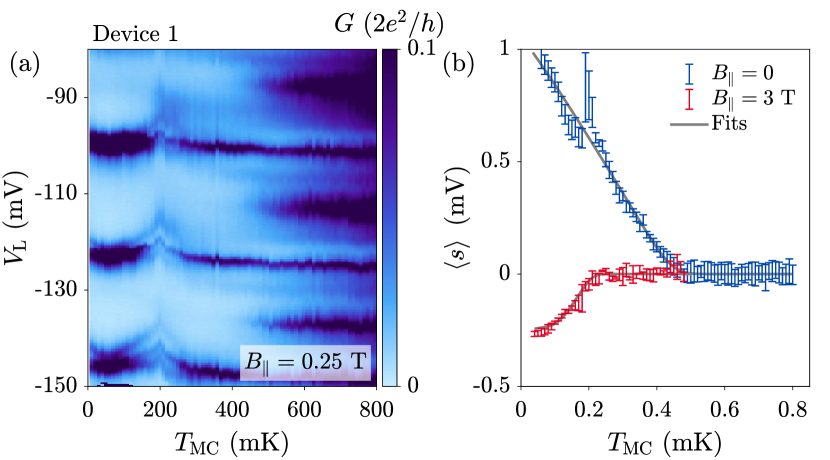
Fig. S.2(a) shows the mixing chamber temperature () dependence of the conductance for the regime shown in Fig. 2 of the Main Text, measured at magnetic field T to induce a finite sub-gap density of states in the contacts. A common mode peak motion versus , which was also observed in the normal state, has been removed. Figure S.2(b) shows the relative peak spacing for the data shown in Fig. S.2(a) and for the regime described in the Main Text with reference to Fig. 3(c).
The conventional expression for the free energy of a superconductor modified to include a sub-gap state is Lafarge et al. (1993); Higginbotham et al. (2015):
| (S.2) |
where is the the first Bessel function, is the spacing for even (odd) valleys, is the Boltzmann constant, is the charging energy, and and are the density of states and volume of Al, respectively, which dominates the semiconductor density of states. and are the superconducting gap and the sub-gap state energy which are parameters of the fit. Fitting Eq. S.2 to the data, we obtain eV and eV at and T, respectively, and sub-gap state energy eV. These values are consistent with bias spectroscopy [see Sec. V].
We estimate the quasiparticle density using the expression , where is the temperature, is the superconducting gap, is the Boltzmann constant, is the Al volume and is the effective number of continuum states for Al Higginbotham et al. (2015). Using the lower bounds for the gap and K, we obtain a quasiparticle density at low field and at T.
For the case of a discrete bound state we follow the analysis of Higginbotham et al. Higginbotham et al. (2015) in using negative differential conductance to calculate the tunneling rate into the bound state. We calculate the ratio as -0.3 for the bound state in the main text Figure 4(c), from which we to obtain a quasiparticle tunneling rate of 10 ns Higginbotham et al. (2015). Together with the quasiparticle density, this yields a parity lifetime of approximately s for this bound state.
While this analysis is strictly valid for the case of a discrete sub-gap state, we tentatively apply it to the negative differential conductance that is observed in the regime of Fig. 2 of the Main Text where sub-gap states are absent. We obtain and a quasiparticle tunneling rate ns, and thereby a parity lifetime ms.
V Comparison of bias spectroscopy to spacing analysis
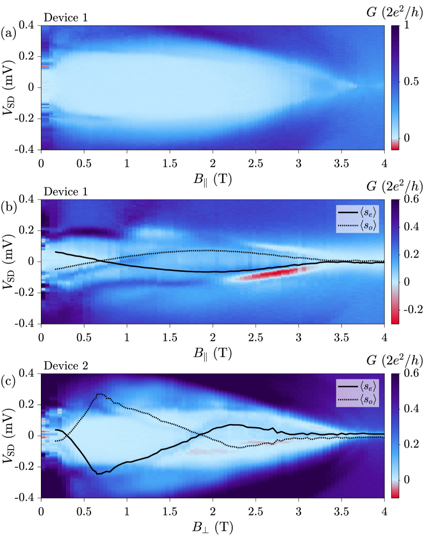
Figure S.3 shows bias spectroscopy of the states described in Figs. 2 and 3 of the Main Text. Figure S.3(a) shows the regime for Fig. 2 of the Main Text when sub-gap states were absent, consistent with this we observed no sub-gap state in bias spectroscopy and a gap that agreed with that extracted from temperature dependence. Figures S.3(b-c) show bias spectroscopy for the states in Figs. 3(c) and (e) of the Main Text overlaid with the sub-gap state energy obtained from the spacing analysis. A finite residual charging energy of the quantum dot reduced the energy resolution when compared that typically observed in tunneling spectroscopy measurements Nichele et al. (2017). Nevertheless, we observed consistency between the spacing analysis and spectroscopy.
VI Sub-gap state dependence on electrostatic gating
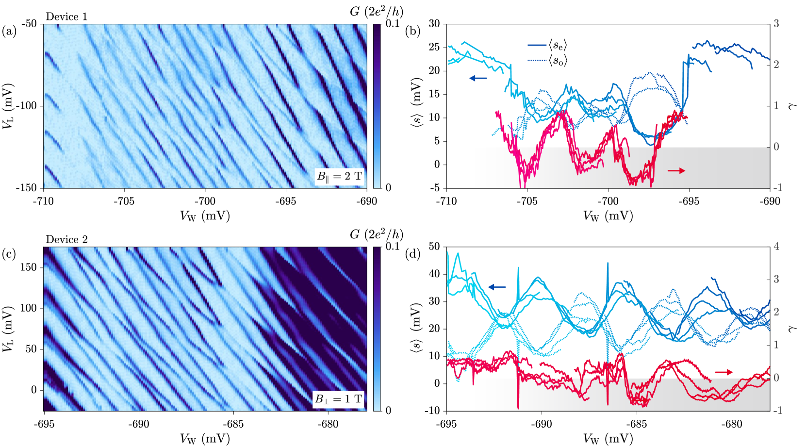
Figure S.4 shows the gate dependence of sub-gap states on for Device 1 2 in the neighborhood of the regimes presented in Fig. 3 of the Main Text. Figure S.4(a) the conductance of Device 1 for T. As described in the Main Text, peaks were split when a sub-gap state entered the spectrum and oscillated around zero-energy as inferred from the spacing, Fig. S.4(b) shows spacing and the conductance ratio for individual pairs of peaks (c.f. the averaged results presented in the Main Text).
Figure S.4(c-d) show similar analysis for Device 2 at , where oscillations were again observed in the spacing and the conductance ratio. Oscillations in the spacing and the conductance ratio show some correlation between features in and , some zero crossings of correspond to maxima in spacing, however the relationship is not robust.
VII Other devices
VII.1 Device 3
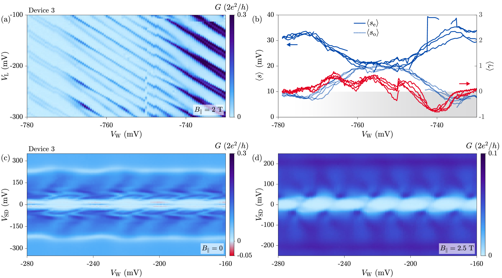
Device 3 is lithographically identical to Devices 1 and 2 presented in the Main Text, i.e. nm nm. In contrast to Devices 1 and 2, Device 3 did not show discrete states in the spectrum. Figure S.5(a) shows vs. for a regime tuned to have no sub-gap state, the superconducting gap closes at T which we attribute to a larger thickness of Al for this device due to variation in processing. Figure S.5(b) shows vs. in a regime where a sub-gap density of states splits the peaks; however, we now show this splitting does not correspond to a discrete sub-gap state.
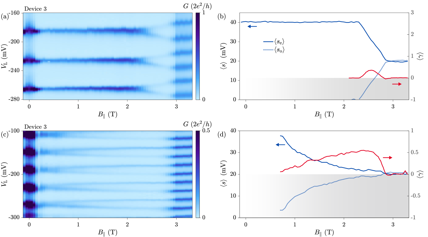
Figure S.6(a) shows shows vs. at T. The spacing splits from to and sticks close to for a range of [Fig. S.6(b)]. However, bias spectroscopy [Fig. S.6(d)] at T in this region showed that this splitting was not due to a discrete state, but rather a continuum, and correlation between and was absent [Fig. S.6(b)].
VII.2 Devices 4 and 5
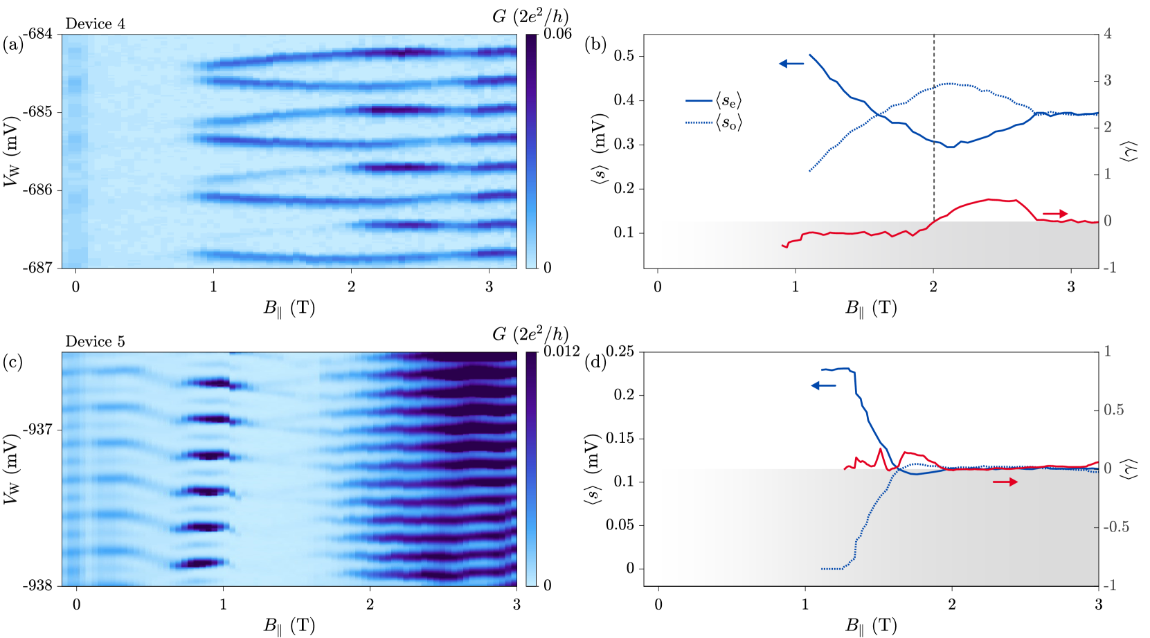
Figures S.7(a-b) show oscillations in for a nm, nm wire where the occupancy was changed by rather than . The oscillations in were qualitatively similar to those presented in the Main Text; oscillations in the conductance ratio vs. were more apparent in this device. The oscillation amplitude of , following conversion to energy units via a lever arm, is eV, significantly smaller than for the 750 nm device in the Main Text (eV).
Finally, figures S.7(c-d) shows oscillations in for a nm, nm wire where the occupancy was also changed by . The oscillations in were negligible in this device. At low field a weak CB peak is observed at spacing, we attribute this to quasiparticle poisoning Albrecht et al. (2017). This poisoning peak disappeared in field prior to the splitting of peaks.
VIII Theoretical comparisons
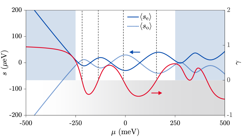
In the Main Text we compare the experimental results to two theoretical models: first, the one-dimensional model of Hansen et al. Hansen et al. (2018) to qualitatively consider oscillations in the quantity ; second, the two-dimensional model of Hell et al. Hell et al. (2017) to quantitatively estimate a bound for the Rashba parameter from the magnitude of the anti-crossing.
The model of Hansen et al. (2018) is a one-dimensional single band model that is used to correlate oscillations in the CB peak conductance to spectral weight transfer between electron and hole-like components of a hybridized MZM. While oscillations in the Zeeman interaction are mainly considered in Ref. Hansen et al. (2018), oscillations as a function chemical potential are also expected. Figure S.8(a) shows theoretical calculations of the conductance ratio and spacing as a function of the chemical potential analogous to the measurements presented in the main text using nm, mev Å for the Rashba parameter, 0.3 meV for the Zeeman interaction and with the chemical potential centered around zero.
To estimate a bound for the Rashba parameter based on the observed anti-crossing we use the model described in Hell et al. (2017):
| (S.3) |
where is the effective mass, is the chemical potential underneath the Al stripe, and are Pauli matrices for particle-hole and spin space respectively, is the Zeeman energy, the -direction is parallel to the wire and the -direction is transverse in the plane of the 2DEG. is a step-like transverse confinement potential, where is the Heaviside step function, the chemical potential is fixed to outside the wire. The dimensions are the same as the experimental dimensions nm and nm, solutions are found on a square lattice with lattice constant 10 nm.
To obtain a bound on , we take the approach of calculating the magnitude of the anti-crossing for various as a function of . For each value of we further constrain the chemical potential in two ways: first, the zero-energy crossing of opposite parity states occurs before the anti-crossing of iso-parity states; second, the energy of the lowest sub-gap state is below at . Both constrains are based on experimental observations. Ranges where these conditions are satisfied are denoted by solid red lines in Fig. S.9. We see that in order to meet this condition and to have magnitude within the experimental range eV, we require at least meV Å for the first sub-band [Fig. S.9(a)]. For the second and third sub-bands [Fig. S.9(b)-(c)] a broader range up to higher can satisfy the experimental condition, therefore we take the value for the first sub-band as a lower bound.
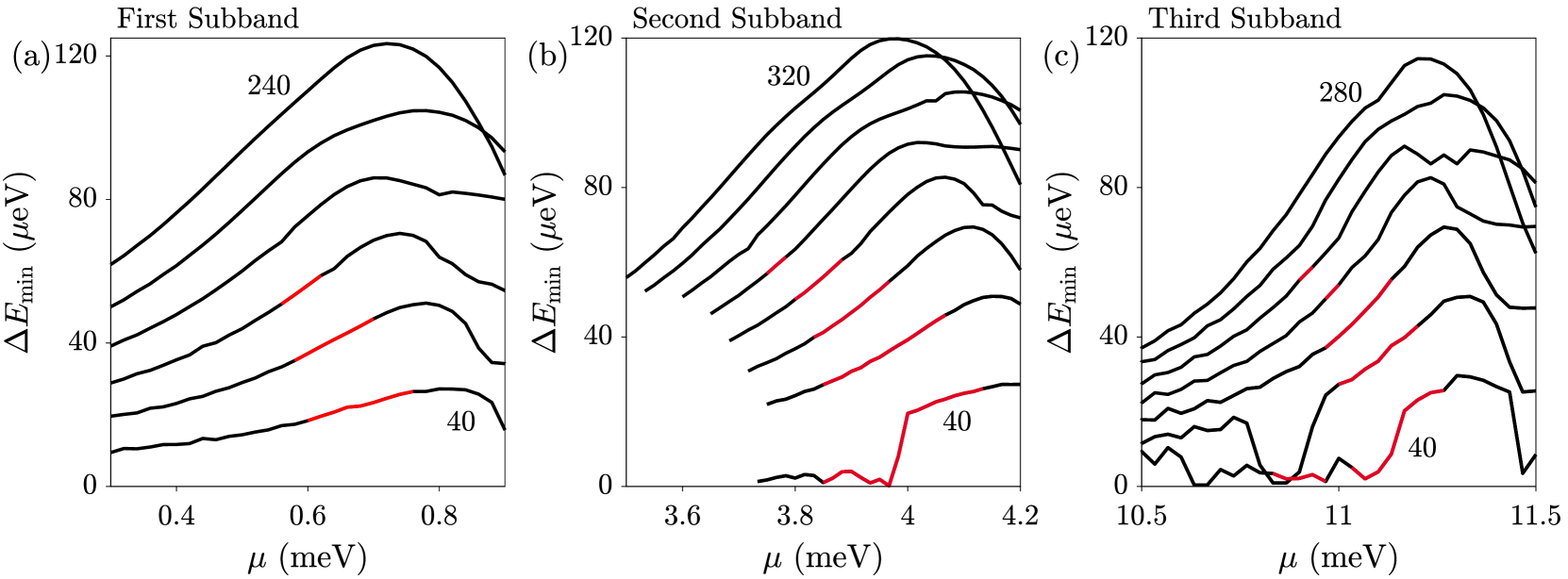
The value of the chemical potential for which the experimental constraints are met i.e. meV is distinct from the 1D case. This is due an offset of the band-bottom energy in the 2D case relative to the 1D case. In the 1D case, the band bottom is at . In the 2D case, there is an additional shift of from the transverse spin-orbit term. In addition, there is a shift due to the transverse confinement energy term which is explicitly included in the 2D model. The precise value of this confinement energy depends on the microscopic details of the heterostructure (and the number of the subband considered) and we therefore do not attempt to correct for this between the 1D and 2D models.
References
- Lutchyn et al. (2010) R. M. Lutchyn, J. D. Sau, and S. Das Sarma, Phys. Rev. Lett. 105, 077001 (2010).
- Oreg et al. (2010) Y. Oreg, G. Refael, and F. von Oppen, Phys. Rev. Lett. 105, 177002 (2010).
- Mourik et al. (2012) V. Mourik, K. Zuo, S. M. Frolov, S. Plissard, E. Bakkers, and L. P. Kouwenhoven, Science 336, 1003 (2012).
- Deng et al. (2016) M. Deng, S. Vaitiekėnas, E. B. Hansen, J. Danon, M. Leijnse, K. Flensberg, J. Nygård, P. Krogstrup, and C. M. Marcus, Science 354, 1557 (2016).
- Nichele et al. (2017) F. Nichele, A. C. C. Drachmann, A. M. Whiticar, E. C. T. O’Farrell, H. J. Suominen, A. Fornieri, T. Wang, G. C. Gardner, C. Thomas, A. T. Hatke, et al., Phys. Rev. Lett. 119, 136803 (2017).
- Zhang et al. (2018) H. Zhang, C.-X. Liu, S. Gazibegovic, D. Xu, J. A. Logan, G. Wang, N. van Loo, J. D. Bommer, M. W. de Moor, D. Car, et al., Nature 556, 74 (2018).
- Aasen et al. (2016) D. Aasen, M. Hell, R. V. Mishmash, A. Higginbotham, J. Danon, M. Leijnse, T. S. Jespersen, J. A. Folk, C. M. Marcus, K. Flensberg, et al., Phys. Rev. X 6, 031016 (2016).
- Tuominen et al. (1992) M. T. Tuominen, J. M. Hergenrother, T. S. Tighe, and M. Tinkham, Phys. Rev. Lett. 69, 1997 (1992).
- Lafarge et al. (1993) P. Lafarge, P. Joyez, D. Esteve, C. Urbina, and M. H. Devoret, Phys. Rev. Lett. 70, 994 (1993).
- Albrecht et al. (2016) S. M. Albrecht, A. Higginbotham, M. Madsen, F. Kuemmeth, T. S. Jespersen, J. Nygård, P. Krogstrup, and C. M. Marcus, Nature 531, 206 (2016).
- Chiu et al. (2017) C.-K. Chiu, J. D. Sau, and S. Das Sarma, Phys. Rev. B 96, 054504 (2017).
- Shabani et al. (2016) J. Shabani, M. Kjaergaard, H. Suominen, Y. Kim, F. Nichele, K. Pakrouski, T. Stankevic, R. M. Lutchyn, P. Krogstrup, R. Feidenhans, et al., Phys. Rev. B 93, 155402 (2016).
- Suominen et al. (2017) H. J. Suominen, M. Kjaergaard, A. R. Hamilton, J. Shabani, C. J. Palmstrøm, C. M. Marcus, and F. Nichele, Phys. Rev. Lett. 119, 176805 (2017).
- Hansen et al. (2018) E. B. Hansen, J. Danon, and K. Flensberg, Phys. Rev. B 97, 041411 (2018).
- (15) See Supplemental Material at [URL] for material and methods, and additional measurements, which include Ref. Shaw et al. (2008); Albrecht et al. (2017).
- Hekking et al. (1993) F. W. J. Hekking, L. I. Glazman, K. A. Matveev, and R. I. Shekhter, Phys. Rev. Lett. 70, 4138 (1993).
- Hell et al. (2017) M. Hell, K. Flensberg, and M. Leijnse, Phys. Rev. B 96, 035444 (2017).
- Bulaev and Loss (2005) D. V. Bulaev and D. Loss, Phys. Rev. B 71, 205324 (2005).
- Takahashi et al. (2010) S. Takahashi, R. S. Deacon, K. Yoshida, A. Oiwa, K. Shibata, K. Hirakawa, Y. Tokura, and S. Tarucha, Phys. Rev. Lett. 104, 246801 (2010).
- Nichele et al. (2014) F. Nichele, S. Chesi, S. Hennel, A. Wittmann, C. Gerl, W. Wegscheider, D. Loss, T. Ihn, and K. Ensslin, Phys. Rev. Lett. 113, 046801 (2014).
- Higginbotham et al. (2015) A. P. Higginbotham, S. M. Albrecht, G. Kiršanskas, W. Chang, F. Kuemmeth, P. Krogstrup, T. S. Jespersen, J. Nygård, K. Flensberg, and C. M. Marcus, Nat. Phys. 11, 1017 (2015).
- Liu et al. (2017) C.-X. Liu, J. D. Sau, T. D. Stanescu, and S. Das Sarma, Phys. Rev. B 96, 075161 (2017).
- Sasaki et al. (2004) S. Sasaki, S. Amaha, N. Asakawa, M. Eto, and S. Tarucha, Phys. Rev. Lett. 93, 017205 (2004).
- (24) J. Shen, S. Heedt, F. Borsoi, B. van Heck, S. Gazibegovic, R. L. M. Op het Veld, D. Car, J. A. Logan, M. Pendharkar, G. Wang, D. Xu, A. Geresdi, C. J. Palmstrøm, E. P. A. M. Bakkers, and L. P. Kouwenhoven, arXiv:1804.08405 .
- Shaw et al. (2008) M. D. Shaw, R. M. Lutchyn, P. Delsing, and P. M. Echternach, Phys. Rev. B 78, 024503 (2008).
- Albrecht et al. (2017) S. M. Albrecht, E. B. Hansen, A. P. Higginbotham, F. Kuemmeth, T. S. Jespersen, J. Nygârd, P. Krogstrup, J. Danon, K. Flensberg, and C. M. Marcus, Phys. Rev. Lett. 118, 137701 (2017).