pnasresearcharticle \leadauthorYao \significancestatementInterlayer interaction in van der Waals heterostructures could induce many exotic phenomena. Unlike commensurate heterostructures, incommensurate ones have often been neglected, due to the rarity in nature and the assumption of suppressed coherent interlayer movement of electrons. How the interlayer interaction affects the electronic structure of such non-periodic heterostructure is a fundamental question. In this work, by successfully growing 30°-tBLG as an example for incommensurate “heterostructure” with quasicrystalline order, we report the emergence of novel mirrored Dirac cones. We identify that these mirrored Dirac cones are a consequence of the interlayer interaction, showing its importance in the incommensurate structure which has been overlooked before. These results broaden the application range of van der Waals heterostructure for future electronic devices. \authorcontributionsAuthor contributions: S.Z. conceived the research project. W.Y. prepared the graphene sample. W.Y. and K.Z. performed the Raman measurements. W.Y. and E.W. performed the conventional ARPES measurements. E.W. and C.B. performed Nano-ARPES measurements and analyzed the ARPES data with assistance from C.C., J.A. and M.C.A. Y.Z., K.B., C.K.C. and J.Z. performed the theoretical calculation. W.Y., J.Z. and S.Z. wrote the manuscript, and all authors commented on the manuscript. \authordeclarationThe authors declare no conflict of interest. \correspondingauthor1To whom correspondence should be addressed. E-mail: jyzhu@phy.cuhk.edu.hk and syzhou@mail.tsinghua.edu.cn.
Quasicrystalline 30° Twisted Bilayer Graphene as an Incommensurate Superlattice with Strong Interlayer Coupling
Abstract
The interlayer coupling can be used to engineer the electronic structure of van der Waals heterostructures (superlattices) to obtain properties that are not possible in a single material. So far research in heterostructures has been focused on commensurate superlattices with a long-ranged Moiré period. Incommensurate heterostructures with rotational symmetry but not translational symmetry (in analogy to quasicrystals) are not only rare in nature, but also the interlayer interaction has often been assumed to be negligible due to the lack of phase coherence. Here we report the successful growth of quasicrystalline 30° twisted bilayer graphene (30°-tBLG) which is stabilized by the Pt(111) substrate, and reveal its electronic structure. The 30°-tBLG is confirmed by low energy electron diffraction and the intervalley double-resonance Raman mode at 1383 cm-1. Moreover, the emergence of mirrored Dirac cones inside the Brillouin zone of each graphene layer and a gap opening at the zone boundary suggest that these two graphene layers are coupled via a generalized Umklapp scattering mechanism, i.e. scattering of Dirac cone in one graphene layer by the reciprocal lattice vector of the other graphene layer. Our work highlights the important role of interlayer coupling in incommensurate quasicrystalline superlattices, thereby extending band structure engineering to incommensurate superstructures.
keywords:
Twisted bilayer graphene NanoARPES Band structure engineering Incommensurate van der Waals heterostructure QuasicrystalThis manuscript was compiled on
-2pt
In van der Waals heterostructures (1), a long-ranged commensurate Moiré superlattice (2, 3, 4, 5, 6, 7) forms only when satisfying +=+ (8), where and are primitive lattice vectors for the top and bottom layers respectively, and , , , are integers. Twisted bilayer graphene (tBLG) can be viewed as a simple version of “hetero”-structure with rotated by a twisting angle with respect to . In tBLG, commensuration occurs when satisfies (9, 10)
| (1) |
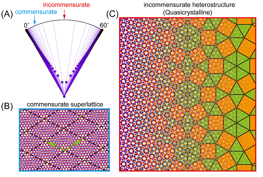
where and are two coprime positive integers. Figure 1(A) plots the possible twisting angles for forming commensurate tBLG for . It is clear that commensuration easily forms around 0° while for larger twist angles, especially around 30°, incommensurate superlattice is more common (11). In contrast to commensurate superlattice with a long-ranged period (see example in Fig. 1(B)), incommensurate superlattice lacks a long-ranged translational symmetry in real space while preserving the rotational symmetry, e.g. 30°-tBLG (Fig. 1(C)) is similar to quasicrystals with a classic dodecagonal pattern (12).
Although the electronic structures of commensurate heterostructures have been investigated in recent years (13, 14, 15, 16, 17), research on incommensurate heterostructures remains limited for two reasons. On one hand, incommensurate heterostructures are difficult to be stabilized and thus they are quite rare under natural growth conditions. On the other hand, it is usually assumed that the interlayer interaction is suppressed due to the lack of phase coherence. For example, incommensurate tBLG has often been taken as a trivial combination of two non-interacting graphene layers (18, 19, 20). How the electronic structure is modified in such incommensurate heterostructures, with symmetry analogous to quasicrystalline order, is a fundamental question. Here by growing epitaxial 30°-tBLG successfully on Pt(111) substrate and revealing its electronic structure using angle-resolved photoemission spectroscopy (ARPES) and NanoARPES, we show that the interlayer coupling can modify the electronic structure significantly, leading to mirrored Dirac cones. Additionally, to understand the intriguing stability that is against common belief on bilayer graphene, we performed first-principles calculations and found that such incommensurate 30°-tBLG heterostructure is stabilized under appropriate substrate conditions.
Results
Growth of 30°-tBLG
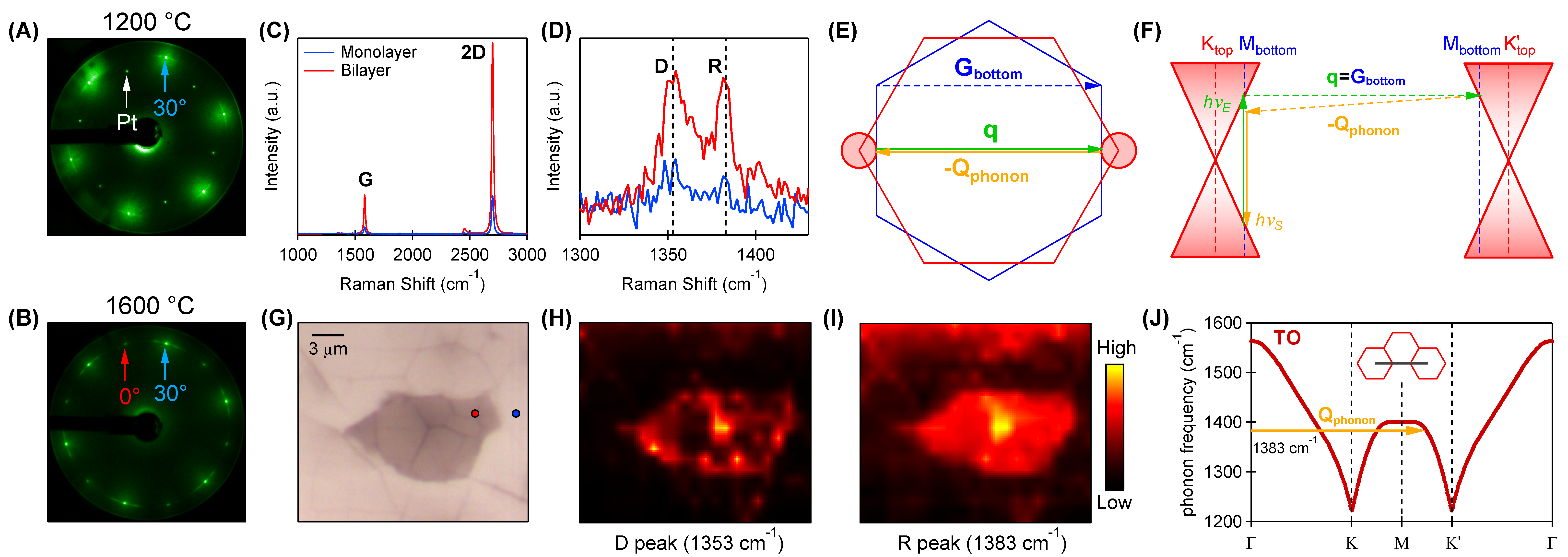
The 30°-tBLG sample was grown on Pt(111) substrate by carbon segregation from the bulk substrate (21, 22). Figure 2(A) shows the low energy electron diffraction (LEED) of bottom monolayer graphene at 30° azimuthal orientation (blue arrow) relative to the substrate. Our previous work shows that distinguished from other graphene/Pt with commensurate (e.g. 22, 33) Moiré superstructures (21), the interface between the 30° monolayer graphene and the Pt(111) substrate is incommensurate without forming any Moiré pattern, leading to nearly free-standing monolayer graphene (22). Further increasing the annealing temperature and time can lead to thicker graphene sample with a new set of diffraction peaks emerging at 0° orientation (red arrow in Fig. 2(B)) coexisting with those at 30°, and such graphene sample is the focus of current work. The lattice constants extracted from LEED show that there is negligible strain (<0.2, see Fig. S1 in SI Appendix for details) between the 30° and 0° graphene layers, and the absence of additional reconstructed diffraction spots in the LEED pattern further supports that they do not form commensurate superlattice. If these diffraction peaks come from the same graphene domains, this would imply that 0° graphene is stacked on top of the bottom 30° graphene layer, namely, a 30°-tBLG is formed. In the following, we will provide direct experimental evidence for the conjectured incommensurate 30°-tBLG from Raman spectroscopy and reveal its electronic structure from ARPES measurements.
Intervalley double-resonance Raman mode
Raman spectroscopy is a powerful tool for characterizing the vibrational mode in graphene (23) and can provide direct information about the sample thickness and stacking. Figure 2(G) shows a typical optical image of the as-grown sample. The optical image shows strong intensity contrast, with a darker region of 10 m overlapping with the brighter region. The Raman spectra in Fig. 2(C) show stronger intensity for the darker region (red curve) than the brighter region (blue curve), suggesting that the darker region is thicker. The spectra for both regions show characteristic features of monolayer graphene (23), in which the 2D mode shows a single Lorentzian peak with stronger intensity than the G mode. This suggests that the top and bottom flakes are both monolayer graphene, and the thicker region is not a Bernal (AB stacking) bilayer graphene, but a bilayer graphene with a large twisting angle instead (24). More importantly, when zooming in the spectra between 1300 to 1430 cm-1, the bilayer region shows two peaks centered at 1353 cm-1 and 1383 cm-1 respectively (Fig. 2(D)). The peak at 1353 cm-1 is the D mode of graphene which is caused by the limited size or defects (23). The Raman mapping for this peak (Fig. 2(H)) shows that it only appears at the edges of the bilayer region or defect centers, consistent with the nature of the D peak. In contrast, the peak at 1383 cm-1 (“R” peak) is observed in the whole bilayer graphene region (Fig. 2(I)), indicating that it is intrinsic to the twisted bilayer graphene.
Since the energy of the R mode is close to that of the D mode, the R mode likely has similar origin as the D mode: intervalley double-resonance (DR) Raman process (25, 26). The key process for the intervalley DR Raman process involves a special scattering process (by defect, phonon or Moiré pattern etc.) in which photoexcited electrons at one valley are scattered to another valley by a non-zero momentum transfer and subsequently decay back to the original valley by emitting a phonon with wave vector = (see Fig. 2(F)). While D mode is induced by defect scattering between two neighboring Dirac cones, instead, we claim that the R mode in our case is caused by scattering between two opposite Dirac cones which are connected by one reciprocal lattice vector of the bottom graphene layer with = (see Fig. 2(E) and 2(F)). This is verified by observing a phonon mode with matching momentum and energy in the transverse optical (TO) phonon spectrum along -K-M-K′- direction (see Fig. 2(J)). The phonon momentum of R mode is not a Moiré reciprocal vector of any commensurate superlattice, suggesting that the bilayer region is an incommensurate 30°-tBLG. It also reveals an unreported scattering process involving the reciprocal lattice vector of the bottom layer in this interesting 30°-tBLG region. This novel scattering process for the observed R mode is closely related to the interlayer interaction to be discussed below and is supported by the exotic electronic structure of the 30°-tBLG which we will investigate next.
Observation of mirrored Dirac cone
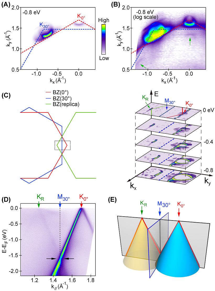
The electronic structure of the sample was first measured by conventional ARPES with a beam size of 100 m. Figure 3(A) shows the ARPES intensity map at -0.8 eV. Characteristic conical contours appear at the K points of the graphene Brillouin zone (BZ) for both 0° and 30° layers (labeled as K and K), in agreement with the coexistence of 0°- and 30°-graphene layers observed in the LEED pattern. Additional contours with weaker intensity are detected inside the first BZ near K (green arrows in Fig. 3(B)) when enhancing the weak features using logarithmic scale. The curvature images (Fig. 3(C)) at different energies with higher visibility show that these contours expand from low to high binding energy similar to the Dirac cones at K, and they occur at the reflected position of K (indicated by green arrow and labeled as KR) with respect to the 30° BZ edges (blue lines). The dispersion near the KR also shows linear behavior, which is the reflected image of the Dirac cone at K (Fig. 3(D)). The mirrored Dirac cone shows similar intensity asymmetry caused by the dipole matrix element (27), with stronger intensity between K (KR) and the M point of the 30° graphene layer M, suggesting that it comes from the original Dirac cone at the opposite momentum valley and is strongly related to the transfer mechanism discussed above for the double-resonance Raman mode (more details are shown in the Discussion section). Moreover, the suppression of intensity at the crossing point M between the original and mirrored Dirac cones indicates a gap opening (pointed by black arrows in Fig. 3(D)). Such mirrored Dirac cones and gap opening are not observed in the bottom monolayer 30°-graphene (see SI Appendix for details). Furthermore, the gap happens to appear at BZ boundary of bottom layer and is away from the substrate bands (see SI Appendix for details), suggesting that they are not caused by the graphene-substrate interaction, but intrinsic properties of the 30°-tBLG. Therefore our ARPES results confirm that the 30° graphene layer spatially overlap with 0° graphene layer and they interact with each other.
The band structures with spatial resolution
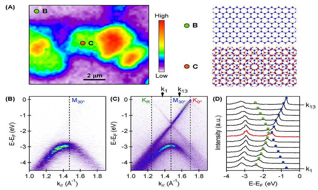
The electronic structure of 30°-tBLG is further confirmed by NanoARPES (28), which is capable of resolving the electronic band structure of coexisting graphene structures with spatial resolution at 120 nanometer scale. A spatially resolved intensity map is shown in Fig. 4(A), where we can distinguish different regions and map out their distinct electronic structure. Region labeled by b shows dispersion along the -M direction of the 30° bottom graphene layer (Fig. 4(B)), while region c shows dispersions from the 30°-tBLG, with dispersion along the -K direction of 0° top graphene layer coexisting with that along the -M direction of the bottom 30° graphene layer (Fig. 4(C)). Therefore, dispersions measured by NanoARPES with spatial resolution provides definitive experimental evidence for the 30°-tBLG, and the mirrored Dirac cones indeed originate from this newly discovered tBLG structure. Moreover, by focusing only in the 30°-tBLG region, sharper dispersions can be obtained and the gap at the M point becomes more obvious. Analysis from the energy distribution curves (EDCs) for 30°-tBLG (Fig. 4(D)) shows a gap at the M point, suggesting the Dirac cone at K and the mirrored Dirac cone are hybridized.
Band gap in k-space
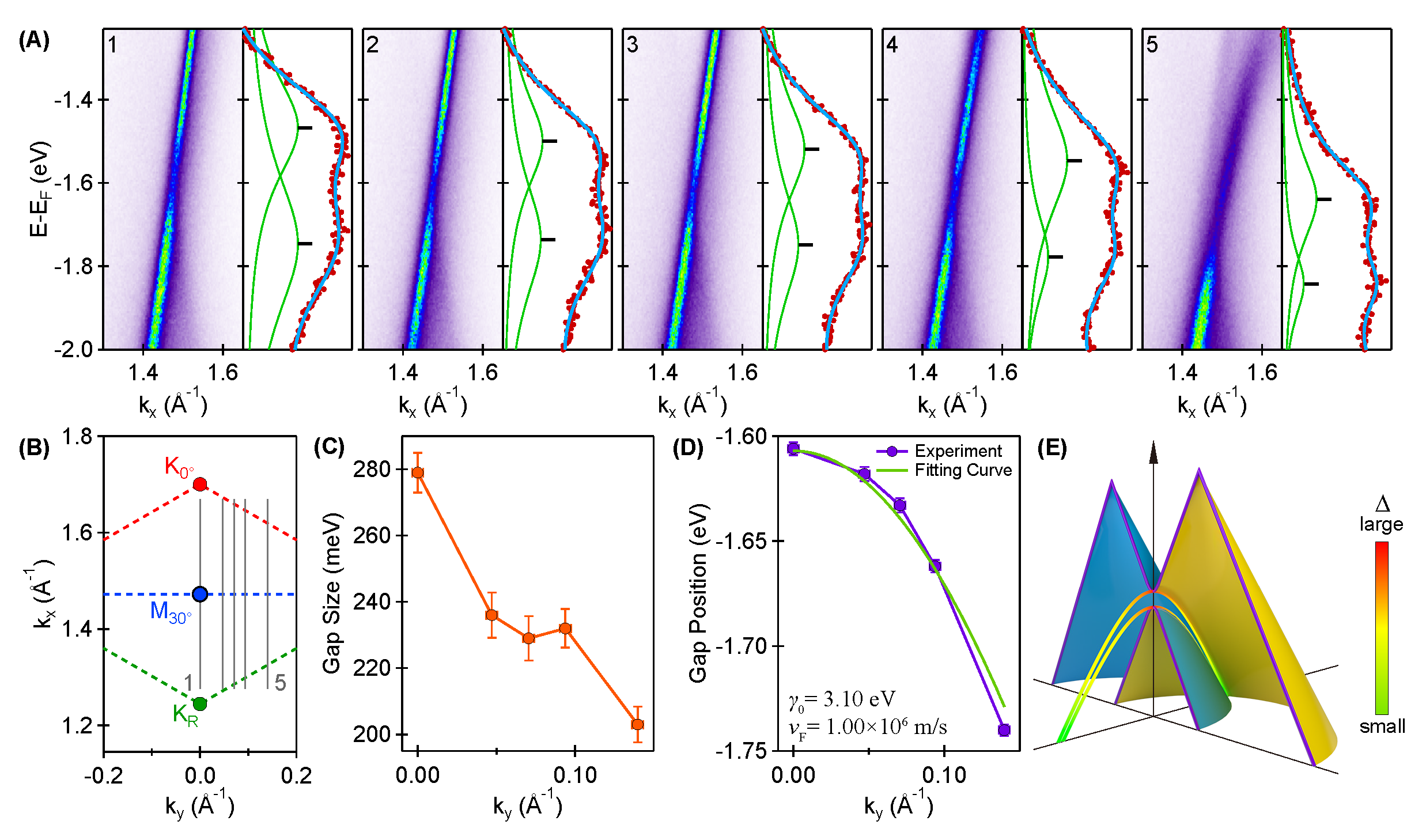
To track the evolution of the gap at the crossing points between the original Dirac cone at K and the mirrored Dirac cone at KR, we show in Fig. 5(A) dispersions measured from cut 1 to 5 (labeled in Fig. 5(B)). The gap size is quantified by the peak separation of the EDCs at the crossing points and the extracted value is plotted in Fig. 5(C). It is clear that the gap size decreases from the maximum value of 280 meV at the M point to 200 meV when deviating from the M point. In addition, we can define the gap position as the average of the two peak positions. The gap position curve in Fig. 5(D) shows that the gap is located at the intersecting line of the two Dirac cones, hence it is possible to fit the gap positions by the energy dispersion obtained from a tight-binding model (see SI Appendix for details). The fitting curve (green curve in Fig. 5(D)) is in good agreement with the experimental data, giving a nearest-neighbor hopping parameter to be 3.10 eV which is closed to the value derived from theoretical calculations (29). The Fermi velocity ( 2.46 Å) is extracted to be 1.0030.002 m/s. A schematic summary of the gap between the original and mirrored Dirac cones is shown in Fig. 5(E).
Theoretical calculation
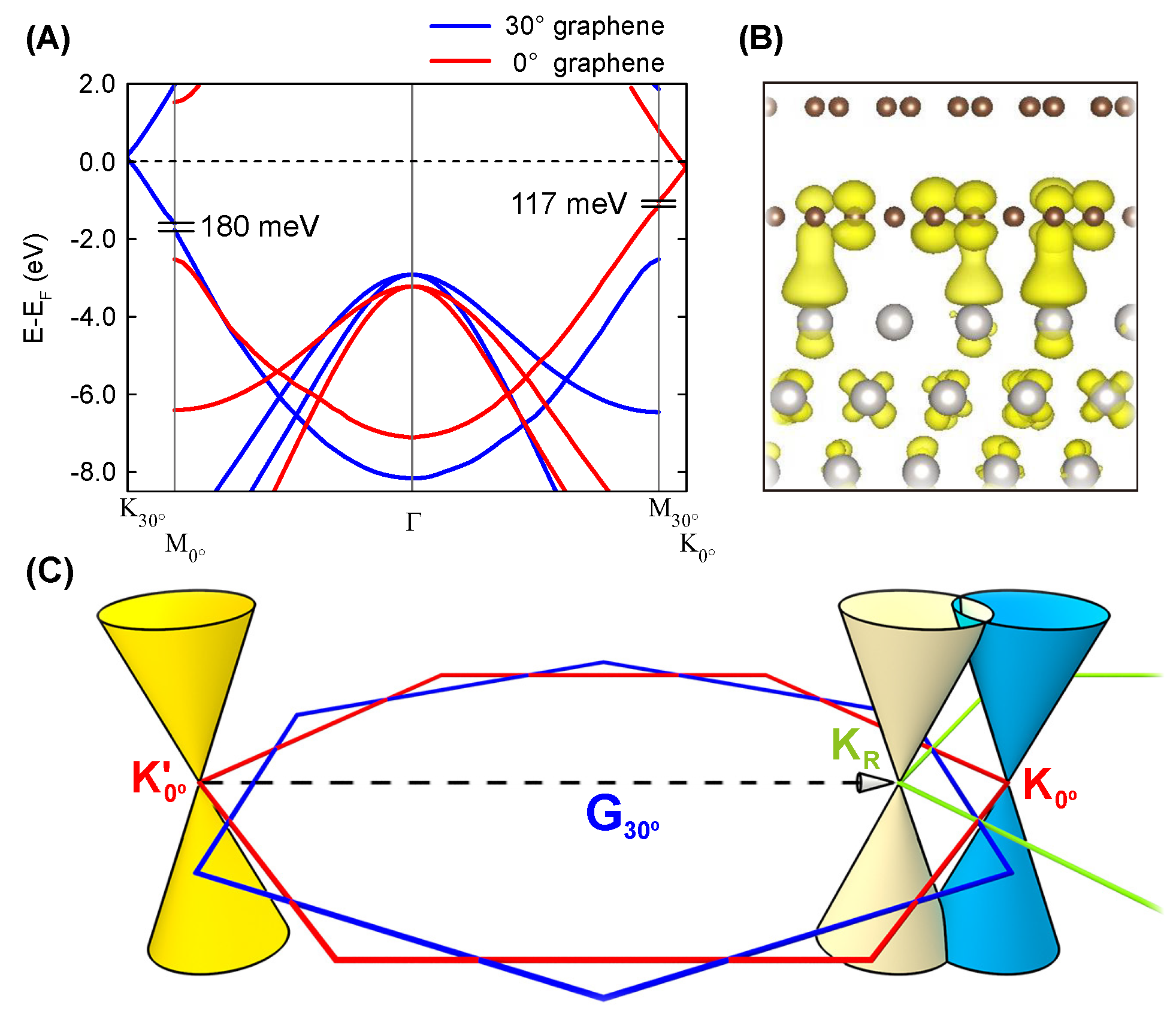
Ab initio calculations are performed to reveal the electronic structure of 30°-tBLG and investigate the stability. Since Bloch theorem does not apply to the non-periodic structure and an infinitely large cell is beyond the calculation capability, a finite supercell of R30° is constructed to mimic the non-periodic 30°-tBLG system. The calculated electronic structure in Fig. 6(A) shows band gap opening at the M point of the counterpart layer, with gap value close to the experimental measurements. An interesting observation regards the stability of 30°-tBLG when the Pt substrate is included in the calculation. While the formation energy of free-standing 30°-tBLG is 1.6 meV/(C atom) higher than the more common AB-stacking BLG, inclusion of the substrate leads to formation energy of 4.1 meV/(C atom) lower than AB-stacking one, which explains why 30°-tBLG emerges in our sample and suggests an important role of the Pt substrate in stabilizing the 30°-tBLG. By investigating real-space projection of the Bloch states, a significant coupling between the carbon p orbital and platinum d orbital (shown in Fig. 6(B)) is revealed near Fermi level. Since such p-d coupling occurs at the point and phase matching between graphene and Pt substrate is less critical (due to zero -vector). Therefore it could thus exist in systems with weak and incoherent sample-substrate interaction such as our sample, contributing positively to the stability of grown 30°-tBLG on Pt substrate. Extrapolating to larger supercell, like 5×5, 7×7 and 16×16, the stability of 30°-tBLG is further enhanced (See SI Appendix for details) and the electronic structure remains similar, suggesting that the calculation conclusion mentioned above still holds at the limit of infinitely large cell or the incommensurate structure. Our calculation, although not perfect, still provides some theoretical insights into the physics and stability of the 30°-tBLG.
Discussion
Unlike the satellite Dirac cones appearing in commensurate graphene system with long-ranged Moiré pattern (30, 31, 32), the emergence of mirrored Dirac cones in incommensurate 30°-tBLG indicates an unusual scattering mechanism in this novel structure. Based on a generalized Umklapp scattering process (33), we build up a tight-binding model with second-order perturbation further included (See SI Appendix for details) and reveal a general coupling condition for two Bloch states in one layer of twisted bilayer system:
| (2) |
where and are wave vectors of the two Bloch states in one layer, and are the reciprocal lattice vectors of the same layer and its counterpart respectively. Applying this condition, we propose a scattering mechanism for electrons in 30°-tBLG: Dirac cone at the K′ point of one graphene layer K is scattered by one reciprocal lattice vector of the other layer , forming a mirrored Dirac cone KR near the opposite momentum valley at K as schematically shown in Fig. 6(C). This corresponds to the simplest case in (2) for and . Such a mechanism is confirmed by three experimental observations. First of all, the momentum of the mirrored Dirac point is connected to the other graphene valley by just one reciprocal lattice vector of the other 30° layer . Secondly, the asymmetry of the intensity contour for the mirrored Dirac cone is identical to the one at K′ (see Fig. 3(D) or Fig. 4(C)), suggesting that the mirrored Dirac cone is scattered from K′ point. Thirdly, such a scattering mechanism is fully consistent with the observed R mode in Raman spectrum. Not only for the incommensurate structure, this scattering mechanism is also able to account for the appearance of replica Dirac cones in those commensurate graphene systems following the same analysis (33). Thus, this mechanism can be applied to other van der Waals heterostructure beyond tBLG.
Conclusions
In summary, we have successfully grown 30°-tBLG, a typical example for incommensurate superlattice with quasicrytalline order. The realization of 30°-tBLG provides new opportunities for investigating the intriguing physics of quasicrystalline superlattice. Moreover, by revealing the mirrored Dirac cones in a 30°-tBLG, we provide direct experimental evidence for the strong interlayer coupling through a coherent scattering process in such an incommensurate superlattice. Such scattering mechanism can be applied to engineer the band structure of both commensurate and incommensurate tBLG as well as other van der Waals heterostructures.
Sample Growth
The graphene sample was obtained by annealing one Pt(111) substrate to about 1600 ℃. At this high temperature, the carbon impurities would segregate from the bulk to surface forming graphene film.
ARPES and NanoARPES
Conventional ARPES measurements were performed at the home laboratory with a Helium discharge lamp and beamline 10.0.1 of Advanced Light Source (ALS) with synchrotron radiation source. The NanoARPES measurements were performed at ANTARES endstation of Synchrotron SOLEIL, France, with a lateral spatial resolution of 120 nm. The sample temperature was kept at 20 K for measurements at ALS and 40 K for those at SOLEIL.
Calculations
The calculations were based on VASP code (34, 35) with plane wave basis set (36, 37). We adopted opt86b-vdW functional (38, 39) to include the van der Waals interactions. A periodic (5×5) on ×R30° structure was created to simulate the 30°-tBLG because it is impossible to directly simulate the very large non-periodic bilayer. The lower layer is slightly compressed about 1.8% to fit the Pt lattice and the upper layer is slightly stretched about 2% to partially compensate the compression from the lower layer. Extensive convergence tests have been performed in terms of vacuum, film thickness, and k-point sampling. Although our calculations were based on one periodic structure, such effects would be extrapolated to non-periodic structures of 30°-tBLG.
This work is supported by the Ministry of Science and Technology of China (Grant No. 2016YFA0303004 and 2015CB921001), National Natural Science Foundation of China (Grant No. 11334006 and 11725418), Science Challenge Project (No. 20164500122) and Beijing Advanced Innovation Center for Future Chip (ICFC).
The Synchrotron SOLEIL is supported by the Centre National de la Recherche Scientifique (CNRS) and the Commissariat à l′Energie Atomique et aux Energies Alternatives (CEA), France. This work is supported by a public grant overseen by the French National Research Agency (ANR) as part of the “Investissements d′Avenir” program (Labex NanoSaclay, reference: ANR-10-LABX-0035), as well as the the French Ministre des affaires trangres et europennes (MAEE), the Centre National de la Recherche Scientifique (CNRS) through the ICT-ASIA programme grant 3226/DGM/ATT/RECH.
References
- (1) Geim AK, Grigorieva IV (2013) Van der Waals heterostructures. Nature 499:419.
- (2) Dean CR, et al. (2010) Boron nitride substrates for high-quality graphene electronics. Nat Nano 5(10):722–726.
- (3) Xue J, et al. (2011) Scanning tunnelling microscopy and spectroscopy of ultra-flat graphene on hexagonal boron nitride. Nat. Mater. 10(4):282–285.
- (4) Dean CR, et al. (2013) Hofstadter’s butterfly and the fractal quantum Hall effect in Moiré superlattices. Nature 497(7451):598–602.
- (5) Hunt B, et al. (2013) Massive Dirac fermions and Hofstadter butterfly in a van der Waals heterostructure. Science 340(6139):1427–1430.
- (6) Yu GL, et al. (2014) Hierarchy of Hofstadter states and replica quantum Hall ferromagnetism in graphene superlattices. Nat. Phys. 10(7):525–529.
- (7) Wang E, et al. (2016) Gaps induced by inversion symmetry breaking and second-generation Dirac cones in graphene/hexagonal boron nitride. Nat. Phys. 12(12):1111–1115.
- (8) Moon P, Koshino M (2012) Energy spectrum and quantum Hall effect in twisted bilayer graphene. Phys. Rev. B 85(19):195458.
- (9) Mele EJ (2010) Commensuration and interlayer coherence in twisted bilayer graphene. Phys. Rev. B 81:161405(R).
- (10) dos Santos JMBL, Peres NMR, Neto AHC (2012) Continuum model of the twisted graphene bilayer. Phys. Rev. B 86:155449.
- (11) Woods CR, et al. (2014) Commensurate–incommensurate transition in graphene on hexagonal boron nitride. Nat. Phys. 10:451–456.
- (12) Koren E, Duerig U (2016) Superlubricity in quasicrystalline twisted bilayer graphene. Phys. Rev. B 93:201404(R).
- (13) Li G, et al. (2010) Observation of van Hove singularities in twisted graphene layers. Nature Physics 6:109.
- (14) Luican A, et al. (2011) Single-layer behavior and its breakdown in twisted graphene layers. Phys. Rev. Lett. 106:126802.
- (15) Ohta T, et al. (2012) Evidence for interlayer coupling and Moiré periodic potentials in twisted bilayer graphene. Phys. Rev. Lett. 109:186807.
- (16) Kandyba V, Yablonskikh M, Barinov A (2015) Spectroscopic characterization of charge carrier anisotropic motion in twisted few-layer graphene. Scientific Reports 5:16388.
- (17) Razado-Colambo I, et al. (2016) NanoARPES of twisted bilayer graphene on SiC: absence of velocity renormalization for small angles. Scientific Reports 6:27261.
- (18) Sprinkle M, et al. (2009) First direct observation of a nearly ideal graphene band structure. Phys. Rev. Lett. 103(22):226803.
- (19) Hass J, et al. (2008) Why multilayer graphene on 4H-SiC() behaves like a single sheet of graphene. Phys. Rev. Lett. 100(12):125504.
- (20) Kim Y, et al. (2013) Breakdown of the interlayer coherence in twisted bilayer graphene. Phys. Rev. Lett. 110:096602.
- (21) Sutter P, Sadowski JT, Sutter E (2009) Graphene on Pt(111): Growth and substrate interaction. Phys. Rev. B 80:245411.
- (22) Yao W, et al. (2015) Monolayer charge-neutral graphene on platinum with extremely weak electron-phonon coupling. Phys. Rev. B 92:115421.
- (23) Ferrari AC, et al. (2006) Raman spectrum of graphene and graphene layers. Phys. Rev. Lett. 97:187401.
- (24) Kim K, et al. (2012) Raman spectroscopy study of rotated double-layer graphene: Misorientation-angle dependence of electronic structure. Phys. Rev. Lett. 108:246103.
- (25) Thomsen C, Reich S (2000) Double resonant raman scattering in graphite. Phys. Rev. Lett. 85:5214.
- (26) Carozo V, et al. (2011) Interlayer interaction in general incommensurate atomic layers. Nano Lett. 11:4527–4534.
- (27) Shirley EL, Terminello L, Santoni A, Himpsel F (1995) Brillouin-zone-selection effects in graphite photoelectron angular distributions. Phys. Rev. B 51:13614.
- (28) Bostwick A, Rotenberg E, Avila J, Asensio MC (2012) Zooming in on electronic structure: NanoARPES at SOLEIL and ALS. Synchrotron Radiation News 25(5):19–25.
- (29) Wallace PR (1947) The band theory of graphite. Phys. Rev. 71:622–634.
- (30) Pletikosic I, et al. (2009) Dirac cones and minigaps for graphene on Ir(111). Phys. Rev. Lett. 102:056808.
- (31) Starodub E, et al. (2011) In-plane orientation effects on the electronic structure, stability, and raman scattering of monolayer graphene on Ir(111). Phys. Rev. B 83:125428.
- (32) Wang E, et al. (2016) Gaps induced by inversion symmetry breaking and second-generation dirac cones in graphene/hexagonal boron nitride. Nature Physics 12:1111–1115.
- (33) Koshino M (2015) Interlayer interaction in general incommensurate atomic layers. New J. Phys. 17:015014.
- (34) Kresse G, Hafner J (1994) Ab initio molecular-dynamics simulation of the liquid-metal–amorphous-semiconductor transition in germanium. Phys. Rev. B 49:14251.
- (35) Kresse G, Furthmüller J (1996) Efficiency of ab-initio total energy calculations for metals and semiconductors using a plane-wave basis set. Computational Materials Science 6:15.
- (36) Blöchl PE (1994) Projector augmented-wave method. Phys. Rev. B 50:17953.
- (37) Kresse G, Joubert D (1999) From ultrasoft pseudopotentials to the projector augmented-wave method. Phys. Rev. B 59:1758.
- (38) Lee K, Éamonn D. Murray, Kong L, Lundqvist BI, Langreth DC (2010) Higher-accuracy van der Waals density functional. Phys. Rev. B 82:081101(R).
- (39) Klimeš J, Bowler DR, Michaelides A (2011) Van der Waals density functionals applied to solids. Phys. Rev. B 83:195131.