Pt3Zr(0001): A substrate for growing well-ordered ultrathin zirconia films by oxidation
Abstract
We have studied the surface of pure and oxidized Pt3Zr(0001) by scanning tunneling microscopy (STM), Auger electron microscopy, and density functional theory (DFT). The well-annealed alloy surface shows perfect long-range chemical order. Occasional domain boundaries are probably caused by nonstoichiometry. Pt3Zr exhibits ABAC stacking along [0001]; only the A-terminated surfaces are seen by STM, in agreement with DFT results showing a lower surface energy for the A termination. DFT further predicts a stronger inward relaxation of the surface Zr than for Pt, in spite of the larger atomic size of Zr.
A closed ZrO2 film is obtained by oxidation in mbar O2 at 400 ∘C and post-annealing at C. The oxide consists of an O-Zr-O trilayer, equivalent to a (111) trilayer of the fluorite structure of cubic ZrO2, but contracted laterally. The oxide forms a R23∘ superstructure. The first monolayer of the substrate consists of Pt and contracts, similar to the metastable reconstruction of pure Pt(111). DFT calculations show that the oxide trilayer binds rather weakly to the substrate. In spite of the O-terminated oxide, bonding to the substrate mainly occurs via the Zr atoms in the oxide, which strongly buckle down towards the Pt substrate atoms, if near a Pt position. According to DFT, the oxide has a bandgap; STM indicates that the conduction band minimum lies eV above .
pacs:
68.55.A-, 68.35.bd, 68.37.Ef, 81.65.MqI Introduction
Zirconia (ZrO2) in pure and doped form is an important material in various fields, with applications in engineering (zirconia toughened alumina, ZTA; zirconia-based thermal barrier coatings for gas turbinesAygun ), ceramics for dentistry (tetragonal zirconia polycrystal, TZP),Denry and as a high- dielectric in microelectronics.BauerHiK Zirconia is also a catalyst support and a catalyst on its own.Tanabe ; Steiner With its wide bandgap ( eV), zirconia is a perfect insulator. It remains an electronic insulator, even when it becomes an ionic conductor at high temperatures, or when doped with trivalent metals (Y, Sc) introducing oxygen vacancies. This property forms the basis of its applications in solid-state electrochemistry, where it is an electrolyte in solid-oxide fuel cellsSteele and gas sensors.Goepel The low electric conductivity of zirconia is not only a blessing but also a curse: While the surface properties of ZrO2 are crucial for many of its applications, detailed studies of ZrO2 surfaces are hampered by the fact that electron-based methods like scanning tunneling microscopy (STM) cannot be applied to this material.
To overcome this problem, ultrathin ZrO2 films have been prepared by deposition and oxidation of Zr on a Pt(111) substrate, resulting in (111)-oriented films with cubic fluorite ZrO2 structure Maurice ; Meinel03 ; Meinel04 . On these films, STM images have been successfully acquired, but it was difficult to obtain atomic resolution.Meinel03 ; Meinel04 ; Meinel06 Growing ultrathin films this way is not straightforward because it is difficult to evaporate zirconium: It has a high melting point (too high for evaporation from a heated crucible) and low vapor pressure at the melting point. Thus, evaporation from a rod in standard ultrahigh-vacuum (UHV) electron-beam evaporators is a lengthy process, prone to contamination with impurities from the residual gas.
Another route towards synthesis of ultrathin oxide films is via the oxidation of a suitable metal alloy. Experience from ultrathin alumina films shows that such an alloy should fulfill two criteria: It should be be based on a metal that is rather inert towards to oxidation, and the alloy should only reluctantly liberate the reactive metal, so that it will be oxidized rather slowly, an important prerequisite for the formation of well-ordered oxide films. This is the case for alloys with a low concentration of the reactive metal NapteschnigCuAl , and so-called superalloys, which show strong chemical ordering and high stability, impeding diffusion of the reactive metal from the bulk to the surface [Examples include the well-known alumina films on NiAl(110)LibudaNiAlOx ; KresseScience and Ni3Al(111)Ni3Al ]. In the present work, we use the superalloy Pt3Zr(0001) as such a substrate for the growth of ultrathin ZrO2 films.
Pt3Zr and other AB3 alloys with elements from groups 4 and 9–10 are also called “Engel-Brewer” alloys. It was noted that the average number of electrons per atom in such alloys is , and such a half-filled shell guarantees exceptionally strong bonding.Brewer ; HumeRothery A more “chemical” interpretation for the high stability would consider electron transfer from the electropositive Zr to Pt, emptying the shell of Zr and completely filling that of Pt. Pt3Zr has a high formation energy of kJ/g atom (Ref. Srikrishnan, ) and a melting point of 2427 K, significantly higher than Pt (2042 K) and Zr (2128 K).PtZrLB Pt3Zr crystallizes in the Ni3Ti (D024) structure, shown schematically in Fig. 1. This structure exhibits ABAC stacking; it can be considered a hybrid of the face-centered cubic and hexagonally close-packed structures. With each Zr atom surrounded by Pt neighbors only, the number of bonds between unequal atoms is maximized. This chemical order prevents easy gliding of dislocations, making Ni3Ti-type materials superalloys, whose strength can even increase with temperature (yield strength anomaly).Hagihara
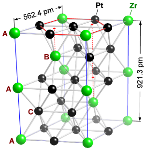
We describe the (0001) surface of this alloy in section III and the preparation and properties of the ultrathin ZrO2 film on this alloy in section IV. The experimental work is supplemented by a density-functional theory (DFT) study of the alloy (section III.2) and the ultrathin oxide (section IV.2).
II Experimental and Computational Methods
The experiments were performed in a two-chamber ultrahigh-vacuum (UHV) system, with a preparation chamber for sputtering, annealing and oxidation, and an analysis chamber for STM and Auger electron spectroscopy (AES). Both chambers had a base pressure below 10-10 mbar. For cleaning we used 2 keV Ar+ ions with a current density between 5 and 10 A cm-2 and typical sputter times of 20 minutes. An electron-beam heater was used for annealing. The thermocouple was attached to the sample holder and not to the single crystal, thus, the thermocouple does not show the correct sample temperature at high temperatures. Temperatures above 800 ∘C were therefore measured with a disappearing-filament pyrometer. For oxidation, we used a directional doser with a microcapillary plate in close proximity to the sample; the pressure at the sample position is estimated as mbar at a chamber pressure of mbar.
The STM images were acquired in constant current mode at room temperature with electrochemically etched W tips; positive voltages refer to tunneling into unoccupied states of the surface (positive sample). We also studied the Fourier transforms of STM images. When both the substrate and the overlayer lattice can be seen in the Fourier transform, it contains essentially the same information as a LEED pattern, except for the spot intensities. Using the Fourier transformed STM image has the advantage that we can select only one domain, while LEED patterns of the oxide are more complex due to the superposition of the mirror domain. For an accurate determination of lattice constants in STM images, we followed the procedure in Ref. deSantisCoO, , based on selected Fourier components transformed back to real space; comparison of the substrate and overlayer lattice in the same image results in an error well below 1%. A cylindrical mirror analyzer with a concentric electron source (3 keV) was used for AES.
The DFT studies were performed with the Vienna Ab-initio Simulation Package (VASP), using the projected augmented wave (PAW) method bloechl1994 ; kressejoubert1999 and an energy cutoff of 400 eV. The generalized gradient approximation (GGA) proposed by Perdew, Burke and ErnzerhofPerdew1996 (PBE) was used to treat the electronic exchange and correlation effects. A -centered Monkhorst-Pack mesh monkhorstpack1976 was used for the calculation of the Pt3Zr bulk properties, and a k-point mesh for the surface calculations. All structures have been relaxed until the residual forces were eV/Å. As we find only a weak interaction between the Pt3Zr surface and the ZrO2 layer, we also investigated the influence of non-local effects within the framework of van-der-Waals DFT (vdW-DF), using the optB88 functional. klimes2011
III The Pt3Zr(0001) surface
III.1 STM results
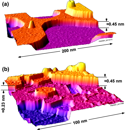
After a few cycles of sputtering and annealing, the Pt3Zr(0001) surface showed large terraces, and AES showed no impurities except for a small concentration of residual oxygen [few % of a monolayer (ML)]. On a well-prepared sample, all steps have a height of nm [Fig. 2(a)]. This indicates that the chemical order is perfect over distances 100 nm, and that only one type of surface termination is present, either A or B/C (cf. Fig. 1). The annealing temperature required for such a surface is C or higher, depending on the history of the sample (see below).
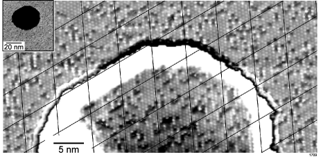
STM images with sufficiently high resolution show a hexagonal array of protrusions with a lattice constant of 0.56 nm, i.e., one protrusion per unit cell of the alloy (Fig. 3). Alloys with strong chemical ordering commonly show a bulk-terminated surface.Varga Comparison with Fig. 1 strongly suggests that the protrusions are Zr, the element with the larger atomic radius (0.16 vs. 0.14 nm for Zr and Pt, respectively). So far, we could not determine whether the missing protrusions in the STM images are antisite defects (Zr replaced by Pt) or Zr atoms appearing dark due do oxygen impurities.
As the step heights of well-annealed defect-free samples are always 0.45 nm or an integer multiple thereof [Fig. 2(a)], the alloy termination layer is either always an A layer or never an A layer (apart from a 180∘ rotation, the B and C layers are equivalent; see Fig. 1). STM images with clearly resolved 0.56 nm alloy lattice on adjacent layers allow us to determine the registry of the surface lattice in these layers. However, it is difficult to extrapolate the lattice across steps, because of drift and image distortions. In case of a hole surrounded by a well-resolved atomic lattice, we can determine the continuation of the surface lattice more easily. Fig. 3 shows that the lattices of Zr atoms in the top layer and at the bottom of the hole are in registry. In the Pt3Zr structure, all A layers have their Zr atoms above each other (Fig. 1); therefore we can conclude that the surface layers are A layers.
Sample preparation can also yield a higher density of steps, some of which are also nm high [Fig. 2(b)]. In addition, we find a network of lines, parallel to the close-packed directions of the metal, i.e., . Some lines appear as protrusions (ridges) with a height of nm, others as depressions with a similar depth. These lines are not observed on well-prepared surfaces, which only exhibit 0.45 nm steps. These ridges are often found at steps, then they pin the steps, and the steps are straight, as opposed to well-prepared samples, where steps can be curved and have any direction. We interpret these lines as domain boundaries of the alloy intersecting the surface.
While heating to high temperature helps reducing the number of such domain boundaries, we found that preparation with an annealing temperature of 900 ∘C can lead to both, well-prepared surfaces and surfaces with a large number of steps and defects (Fig. 2). We could reproducibly avoid the domain boundaries by sputtering not at room temperature (RT) but rather soon after high-temperature annealing, while the sample was cooling from 400 to 100 ∘C (roughly 20 minutes), followed by the final annealing step (without sputtering) at 900 ∘C. We can only speculate about the reason for the different outcome of sputtering at RT or slightly higher temperatures: Any structural of morphological differences between samples sputtered at RT or slightly elevated temperatures should disappear after annealing at 900 ∘C. Thus, differences of surface composition must be responsible for the domain boundaries seen after sputtering at RT. It is well known that preferential sputtering of alloys leads to a modification of the chemical composition, and the composition can depend on the sputtering temperature: At elevated temperatures, the preferentially sputtered element can be replenished at the surface by diffusion, causing depletion of that element over a thicker region of the sample. In addition, preferential sputtering can depend on the roughness of the sample, which also depends on the temperature. Assuming that Pt is preferentially found at steps,woudaPtRh Pt would be sputtered preferentially on rougher samples with many steps, again modifying the surface composition depending on the sample temperature during sputtering. Unfortunately, the differences of surface composition are too small to be detected by AES.
Recently, a phase diagram was constructed from thermodynamical data of the Pt-Zr system.Gao It shows that the Pt3Zr phase has a narrow stability range ( % at 1000 K, even less at lower temperatures), i.e., phase separation occurs at very small deviations from the Pt3Zr stoichiometry. This supports our notion that the sample is sensitive to tiny variations of the stoichiometry. Slight deviations from the ideal stoichiometry do not lead to nucleation of a completely different phase; this would be easily detected by different terrace heights and different atomic structure in STM. Instead, we observe domain boundaries, which are probably enriched in one element.
III.2 DFT study of the Pt3Zr(0001) surface
In order to benchmark the description of the substrate by DFT, we determined the optimal lattice parameters of the Pt3Zr bulk using both the GGA (PBE) and vdW-DF (optB88) functionals. Table 1 shows the results of a fit to a Birch-Murnaghan equation of state, together with the experimental values from Ref. PtZrLB, . The comparison shows that the predicted geometries of the GGA (PBE) and vdW-DF (optB88) are rather similar; both slightly overestimate the experimental lattice parameters, which results in an overestimation of the volume by about 5.5 and 6.1%, respectively.
| PBE | optB88 | exp. | |
|---|---|---|---|
| (pm) | 572.9 | 574.2 | 562.4 |
| (pm) | 936.4 | 938.0 | 921.3 |
| Volume (nm3) | 0.2663 | 0.2678 | 0.2524 |
From the calculated surface energies of the two different terminations of Pt3Zr(0001) we can determine whether the terminating layer should be of A type (fcc) or B/C type (hcp; see Fig. 1). To address this question, we compared the calculated surface energies for two differently terminated 5-layer slabs of Pt3Zr by DFT (PBE functional). The calculations yield a surface energy of 0.73 eV per surface atom for the A-terminated slab (ABACA stacking, as shown in Fig. 1). This is 66 meV lower than for the C-terminated (CABAC stacked) slab. The relative arrangement of the first two layers is the same for both slabs; thus, the 3rd monolayer significantly influences the surface energy, stabilizing the A termination. The DFT result is in agreement with the experimental observation of an A-terminated surface.
The A-terminated Pt3Zr surface (7-layer slab) shows a small rumpling in the top layers. The surface Zr atoms are 15 pm lower than the Pt. In the second monolayer, the Zr is 15 pm higher than the Pt. The distance between the first and the second monolayer is 229.5 pm, and between the second and the third monolayer 236.1 pm (we define the interlayer distances as the difference of the average height of the atoms in each layer). Compared to the calculated bulk value of 234.1 pm, this corresponds to a 1.9% contraction of the first, and a 0.4% expansion of the second interlayer distance. The overall inward relaxation of the first monolayer, followed by a slight outwards relaxation of the 2nd ML is typical for metal surfaces. It is unusual, however, that the larger atom (Zr) in the surface buckles inwards. Nevertheless, the relative relaxations of Pt ( %) and Zr ( % with respect to the bulk interlayer distance of the alloy) in the Pt3Zr(0001) surface are comparable to the pure metals [+1 % and % for Pt(111) Zolyomi and Zr(0001) Kwon , respectively].
We also simulated a surface terminated by a full Pt layer, as observed experimentally after oxidation of the sample (see below). For constructing these Pt-terminated slabs we simply replaced zirconium in the surface layer by platinum. Again we find a higher stability for the A termination; albeit with a low surface energy difference of 6 meV per atom as compared to the B/C termination. Also the Pt-terminated slab shows a slight buckling of the surface: The Pt atoms with a Zr neighbor in the 2nd ML are 7 pm higher than the other Pt surface atoms. Similar to the A-terminated stoichiometric Pt3Zr, the Zr atom of the second monolayer is situated 12 pm closer to the surface than the Pt atoms of the same layer. The first two interlayer distances in the Pt-terminated slab are 229.2 pm and 233.1 pm, i.e., both are contracted with respect to the bulk (by 0.4% and 2.1%, respectively).
IV ZrO2 films on the Pt3Zr(0001)
IV.1 Preparation and experimental investigations
In order to prepare an ultrathin zirconia film at the alloy surface, we oxidized the sample at mbar O2 at 400 ∘C for 30 minutes. This treatment results in many islands, about 0.2 nm in height, and a few holes of nm depth [Fig. 4(a)]. About 30–40% of the surface is covered with islands; the total area of the holes is low (). A flat oxide-covered surface can be obtained by post-annealing at temperatures C. If the annealing temperature is too high, C, the oxide film becomes discontinuous, with a small fraction of uncovered metal; presumably oxygen diffuses into the bulk. This is the only difference between films annealed at different temperatures above 750 ∘C. STM images with atomic resolution are obtained at low tunneling voltages typical for ultrathin oxide films (cf. Ref. KresseScience, ), and the oxide shows good order with a lattice constant of nm [Fig. 4(b)]. The atoms imaged by STM show significant height differences of up to 50 pm; almost every atom has at least one neighbor differing in apparent height by pm.
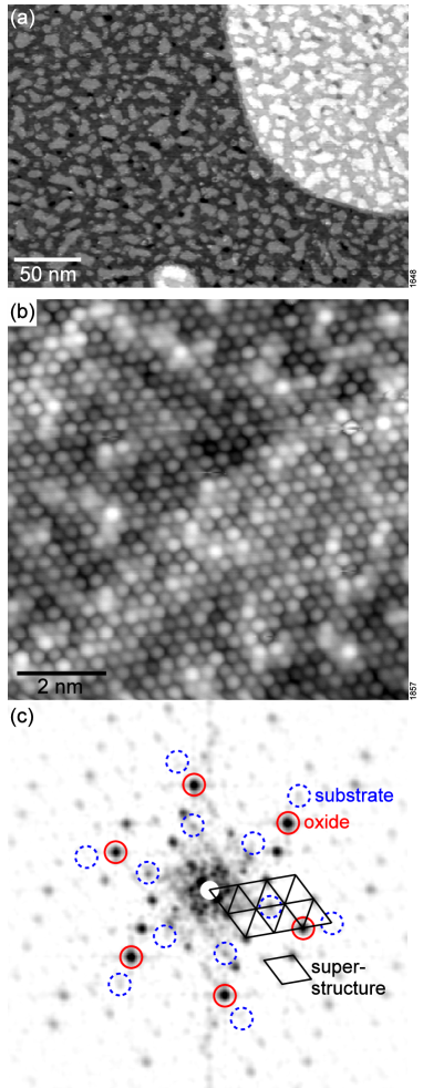
Fig. 4(c) shows the Fourier transform of Fig. 4(b). The spots of the oxide grid are marked by full circles. The outer broken circles correspond to the metal lattice of the substrate ( nm), and the inner broken circles to the unit cell of the ordered alloy ( nm). Not all of these substrate spots are apparent in the Fourier transform, but their positions can be ascertained by comparison with images of the substrate. The superstructure cell (1.2 nm in real space) is marked by black lines. It is commensurate, each Fourier spot of the 0.28 nm substrate lattice and the oxide coincides with the superstructure reciprocal lattice. In terms of the reciprocal lattice of the superstructure, the reciprocal lattices of the oxide and metal have side lengths of and , respectively. Translated to real space, this means that the superstructure has a R cell with respect to the 0.28 nm metal atomic lattice (i.e., not taking into account the chemical order of the alloy), and the lattice constant of the oxide is times that of the metal. The rotation angle between the oxide and the substrate lattice is . The spots of the 0.56 nm alloy lattice appear at half-integer positions with respect to the reciprocal cell of the R superstructure (which was referred to the 0.28 nm lattice). Thus, when including the chemical order of the alloy, the superstructure cell is twice as large in real space (2.4 nm). We have analyzed several STM images of different preparations and always found the same relation between substrate and oxide lattice.
The hexagonal lattice suggests formation of a ZrO2(111) layer, as already found for films grown by deposition and oxidation of Zr on Pt(111)Maurice ; Meinel03 ; Meinel04 ; Meinel06 . The lattice constant of 0.350 nm found by STM is only 3% lower than the interatomic distance in (111) layers of cubic ZrO2 ZrO2Note . The charge-neutral building block of ZrO2(111) is an O-Zr-O trilayer. From STM, we cannot determine the thickness of the oxide, i.e., whether one or more such trilayers are present.
To this end we compare the oxygen Auger signal of the ZrO2 films with that of a RhO2/Rh(111) trilayer oxide, which has a well-known structure with an in-plane lattice constant of 0.310 nm as determined by surface x-ray diffraction.GustafsonRh111 In contrast to the RhO2 trilayer oxide, AES measurements of the ultrathin zirconia films are hampered by strong electron-stimulated desorption (ESD) of oxygen; we observe a 10% decrease of the oxygen signal within 50 seconds. Correcting for ESD by extrapolating the oxygen signal back to the start of the measurement we obtain a ratio between the oxygen signals of the zirconia film and the RhO2 trilayer of . This is slightly less than expected on the basis of the areal densities of the two oxides, . The discrepancy might be related to a shoulder observed at the high-energy side of the oxygen peak of RhO2, which amounts to 15% of the total O signal; the shoulder is possibly due to oxygen dissolved in the Rh bulk. Nevertheless, these AES results clearly rule out the possibility of a ZrO2 film thicker than a single trilayer. As our STM images always show the same superstructure and appearance of the oxide we conclude that the zirconia film always consists of a single trilayer.
During growth of the ultrathin zirconia film, Zr is liberated from the alloy. Defining 1 ML (monolayer) as the density of atoms in the alloy surface, each layer of the alloy contains 0.25 ML Zr. To form the oxide, we need ML Zr. Counting all metal atoms irrespective of their identity, this means that 64% of the upper monolayer is removed. The remaining 36% of the surface layer are present as islands unless mobility is high enough for mass transport to or from steps [cf. Fig. 4(a)]. Mass transport of Zr into the oxide layer also results in a Pt-enriched near-surface region of the alloy. The narrow range for the Pt3Zr structure in the phase diagram (mentioned above, cf. Ref. Gao, ) suggests that replenishing the missing Zr needs long diffusion paths to keep the alloy composition within the Pt3Zr stability range. Such long-distance diffusion will need extremely high temperatures, otherwise the alloy surface remains Pt rich. The amount of Zr needed for creation of the oxide layer corresponds to the Zr content within ML of the alloy.
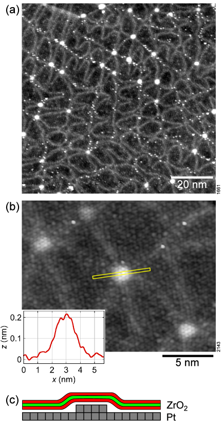
The presence of at least one Pt layer below the oxide also explains the pattern of weak ridges on the surface [Fig. 5(a)]. Pt(111) is know to be on the verge of reconstruction,MichelyPt111rec where the first ML contracts in a manner similar to Au(111). With an interatomic distance of 0.281 nm, the alloy lattice is larger than that of pure Pt (0.2775 nm), so it is natural that the first Pt layer contracts with respect to the underlying bulk lattice. As is usual for structures consisting of a first layer with a lattice constant smaller than the underlying bulk, the bright ridges mark the positions where the first-layer (Pt) atoms are located in bridge sites of underlying substrate lattice. The alternating wide and narrow dark regions between the ridges indicate that one of the two stacking sequences (Pt in hcp or fcc hollow sites) is preferred.
Our STM images also show small nm high protrusions in the oxide lattice [Fig. 5(b), see also the linescan in the inset]. These protrusions are always found at the nodes of the Pt dislocation network. The height of these protrusions is close to that of a metal layer, suggesting that these protrusions are caused by a small metal island below the oxide. In contrast to normal substrate steps, where we see a rather sharp boundary, the oxide lattice runs smoothly over these protrusions like a carpet [Fig. 5(c)]. This observation and the fact that such defects should quickly disappear at the annealing temperature indicates that these are metal islands resulting from expulsion of metal atoms from the surface while cooling to room temperature. Possibly this is caused by a lower coefficient of thermal expansion of the dense (thus hard), reconstructed Pt(111) layer compared to the bulk of the alloy. The junctions of the dislocation lines mark points where dislocations reach the surface; these sites should be nucleation sites for any metal atoms diffusing beneath the oxide carpet at high temperature, and, in addition, the more weakly bound metal atoms at these defect sites should be also the first ones to get expelled when the Pt layer contracts.
We further observe a few bright atom-sized defects in the oxide [e.g., two near the top right corner of Fig. 5(b)]. These defects also show a clear correlation with the ridges (dislocations) of the Pt reconstruction. The nature of these point defects is unclear.
Fourier transforms [Fig. 4(c)] show spots in the positions corresponding to the 0.56 nm lattice of the ordered alloy; in some STM images (especially when taken at positive sample bias) this is even the dominating Fourier component. For a thick Pt layer on top of the ordered alloy the 0.56 nm modulation should be smoothed out; thus, the Pt layer is probably only one ML thick, and the second substrate layer is already an ordered alloy.
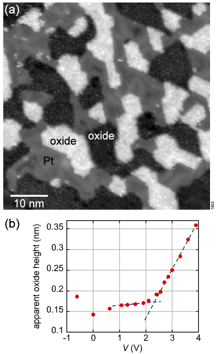
Shorter oxidation (5 instead of 30 minutes), and no post-annealing results in a surface partially covered by oxide. The O/Pt AES peak ratio of this surface was roughly half of that of a fully-oxidized high-temperature annealed sample, and STM shows % bare metal surface [Fig. 6(a)]. It is interesting to note that the uncovered metal surface also shows the dislocation lines of the Pt reconstruction [only weakly visible in Fig. 6(a) because of their low corrugation compared to the step heights]. Thus, the first monolayer consists of Pt in the uncovered areas as well; the amount of Zr needed for formation of the incomplete oxide layer is still higher than that in one monolayer of the alloy. The Pt surface also shows height modulations due to the 0.56 nm lattice of the underlying alloy.
Fig. 6(a) shows two levels of oxide (bright and very dark gray); the height difference equals one metal interlayer distance (0.23 nm). This is a consequence of mass transport due to the different metal densities in the alloy and the oxide.
We now focus on the electronic properties of the oxide. A first impression of its metallic or insulating nature can be gained by studying the apparent height of the oxide on the metal as a function of tunneling voltage. When tunneling into the band gap, an ultrathin insulator appears thinner than its geometric height. Bertrams ; Hebenstreit When tunneling into states above the conduction band minimum, the apparent height strongly increases. Napetschnig The sample with partial oxide coverage [Fig. 6(a)] allows us to compare the apparent height of the oxide with that of the metal substrate (Pt terminated). The apparent height of the oxide increases very slowly at low voltages; above V the height rises sharply and almost linearly [Fig. 6(b)]. This behavior is very similar to the one observed for ultrathin alumina films on NiAl(110).Napetschnig From the intercept of the two broken lines in Fig. 6(b), we estimate that the conduction band minimum of the oxide is at eV above the Fermi level.
IV.2 DFT study of the ultrathin ZrO2 films
We have first calculated the properties of a free-standing ZrO2(111) trilayer. DFT gives an in-plane lattice constant of 330 pm, 9 % less than the in-plane distances in cubic ZrO2(111) (DFT value: 363.2 pm). The in-plane contraction is accompanied by a 31% expansion perpendicular to the plane, with calculated interlayer distances between the Zr and O layers of 97.4 pm in the trilayer film, compared to 74.1 pm in cubic bulk ZrO2.
To decrease the computational effort involved in calculating the full R superstructure of the ZrO2/Pt3Zr(0001) observed in experiment, we used a smaller model for the DFT calculations. The diagonal of the unit cell of the free-standing ZrO2(111) (572 pm) fits the DFT lattice constant of the alloy ( pm), so we simply use one alloy unit cell with oxide cells on top (Fig. 7). By keeping roughly the lattice constants of the free-standing ZrO2(111) trilayer, this approach overestimates the lateral contraction of the oxide film on the metal substrate; according to our STM data the oxide is contracted by only 3%. The essential properties of the system should nevertheless be reproduced well by the calculations.
We have compared two lateral adsorption configurations of the ZrO2 film (Fig. 7). Either one of the Zr atoms of the trilayer, or one of the the lower oxygen atoms (O1) is positioned on top of a substrate Pt atom. For both configurations, the PBE adsorption energies are low and degenerate within our computational accuracy: 300 meV (Zr above Pt) and 299 meV (O1 above Pt) per ZrO2 formula unit (Table 2). The calculated interlayer distances between the lower O layer (“O1”) of the ZrO2 trilayer and the substrate are large, more than 300 pm, again indicating a very weak adsorption. Nevertheless, the interaction with the substrate induces a slight vertical contraction of the oxide film, with the Zr-O interlayer distances reduced by 2–3 pm compared to the free-standing film, and a slight buckling of the Zr layer. The latter is stronger if a Zr atom sits directly above a Pt atom (configuration “Zr/Pt” in Table 2); this Zr atom moves down, towards the metal substrate. Within the computational accuracy, the buckling of the Pt substrate atoms is the same as in the bare substrate (7 pm).

| Functional | PBE | vdW-DF | ||
|---|---|---|---|---|
| Configuration | O1/Pt | Zr/Pt | O1/Pt | Zr/Pt |
| (pm) | 95 | 95 | 96 | 96 |
| (pm) | 95 | 95 | 95 | 94 |
| (pm) | 349 | 337 | 266 | 244 |
| (pm) | 2 | 9 | 56 | 71 |
| (pm) | 0 | 0 | 5 | 0 |
| (pm) | 8 | 7 | 7 | 1 |
| (meV) | -299 | -300 | -338 | -385 |
As standard DFT neglects non-local contributions, we have performed additional calculations using the van der Waals DFT (vdW-DF), which also gives an improved description for physisorbed overlayers MittendorferGraphene . Indeed, the vdW-DF results in a significantly stronger adsorption. The adsorption energies show a moderate increase by 40–85 meV (O1/Pt and Zr/Pt geometries). More significant is the decrease of the distance to the substrate by 83–93 pm, bringing the substrate-oxide distances closer to typical bond lengths.
The closer distance results in a significant buckling of the Zr layer. In the Zr/Pt geometry, the Zr atom directly above a Pt substrate atom moves down by 47 pm (compared to the center between the O1 and O2 layers). This buckling results in a Pt-Zr distance of 293 pm, which is comparable to the Pt-Zr distance in the alloy ( pm with this functional). In the O1/Pt geometry, the Zr atom in the oxide closest a Pt atom in the substrate buckles down by 35 pm (Pt-Zr distance: 338 pm). This indicates that the oxide film binds to the substrate via the Zr atoms, not the oxygen, even though the O1 atoms reside much closer to the substrate than the Zr. In spite of the large movement of the Zr atom closest to Pt, the force exerted by the Pt-Zr bond is small: The Pt atom directly below the Zr in the oxide moves up by only 5 pm upon adsorption. Thus, the ultrathin oxide is rather soft with respect to distortions of its Zr sublattice. This type of distortion is different from the soft phonon mode leading to instability of cubic bulk ZrO2 below K; there the oxygen atoms are displaced in an initially rigid Zr sublattice souvatzis .
While one Zr atom in the ZrO2 trilayer buckles down, the two others move up by roughly half that amount, keeping the overall O1-Zr and Zr-O2 interlayer distances almost unchanged. This can be explained by in-plane displacements of the O atoms. When a Zr atom directly above a Pt moves down, its three lower oxygen neighbors remain at the same height above the substrate and move laterally away from this Zr to make space. This increases the O-O distance in the triangle below the Zr from 331 to 357 pm. The oxygens above this Zr atom also remain in the same plane, but move closer together (O-O distances 312 pm). Now the other two Zr atoms experience a compressed oxygen layer below and expanded O-O distances above; to keep reasonable Zr-O bond lengths they move up.
In the O1/Pt configuration (vdW-DF geometry), the distance between the on-top O1 atom and the Pt below is 258 pm. This O atom moves down by 5 pm and the Pt atom moves up by 5 pm, indicating that the O-Pt interaction is also attractive, but the resulting O-Pt distance is still significantly larger than a typical O-Pt bond length (204 pm in PtO; Ref. McBride, ). Comparing the bonding energies and the substrate-oxide distances of the Zr/Pt and O1/Pt configurations also shows that the oxide binds much more strongly via its Zr atoms than via the oxygen.
Figure 8 gives an overview of the electronic density of states (DOS) of the ZrO2 film for both, the PBE and vdW-DF configurations. The experimentally observed large cell contains many different lateral positions of the oxide on the substrate, we thus averaged the DOS over the O1/Pt and Zr/Pt simulation cells for each configuration. In both, the PBE and vdW-DF configurations, we find a band gap of about 4 eV for the trilayer oxide. The DOS is essentially zero in the vicinity of . Minor contributions in the band gap arise from hybridization with the metal support. As expected, these contributions are strongest for the lower oxygen atoms (O1, dotted), and increase with decreasing distance to the substrate (from the PBE to the vdW-DF configuration). The DFT calculations predict a conduction band minimum at eV. When comparing this result with the experimental value ( eV; Fig. 6), it should be noted that DFT systematically underestimates band gaps, thus the experimental and calculated values can be considered in reasonably good agreement.
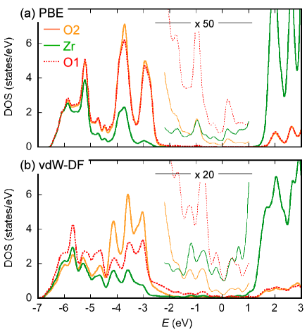
We have also simulated STM images for both, the PBE and the vdW-DF geometry, by plotting the local density of states (LDOS) above the surface between and eV. We find that the highest LDOS is found above the upper atoms (O2) in the PBE geometry, but above the Zr atoms in the vdW-DF geometry. This result is directly related to the DOS near plotted in Fig. 8, where the Zr DOS increases more strongly with decreasing oxide-substrate distance than the O2 DOS (compare the PBE and vdW-DF geometries). The low DOS in the bandgap and the low tunneling resistance used for atomic resolution [Fig. 4(b)] imply a short distance between the tip and the oxide. Together with the soft Zr sublattice mentioned above, we consider it likely that the experimental STM images are dominated by tip-sample interaction. Thus, the LDOS is only of limited value for predicting whether STM shows the oxygen or the Zr atoms as protrusions.
Nevertheless, the STM results help us to decide whether the PBE or vdW-DF functional better describes this system: The large buckling of the oxide seen by STM cannot be reconciled with the PBE results, which predict flat layers for oxygen and Zr. Thus we consider the vdW-DF geometry a more realistic description of the system than PBE. The large buckling observed by STM also indicates that STM shows the Zr atoms as protrusions.
V Conclusions
We have characterized the Pt3Zr(0001) surface by STM and DFT and grown ultrathin ZrO2 films by oxidation of this alloy. The film consists of a O-Zr-O trilayer. Oxidation is self-limiting, similar to ultrathin alumina films obtained by oxidation of NiAl alloys, indicating that O2 cannot dissociate on the trilayer oxide. Incorporation of Zr into the oxide leads to a Pt layer at the interface, which reconstructs by contracting. DFT calculations show that the oxide binds to the substrate via some of its Zr atoms, causing a large rumpling of the Zr layer in the oxide. The O layers remain rather flat and the average height of the Zr layer remains centered between the two O layers. Strong oxide-support bonding via the metal cations is very different from the surface oxides of the late transition metals. All these surface oxides bind to the surface via oxygen,LundgrenJPCM even when the oxygen-metal interlayer distances are much closer than in the ZrO2 film, putting the metal atoms close to the substrate.LundgrenPd111 .
Our study also indicates that DFT-only calculations of an oxide-metal interface can give misleading results; non-local contributions (van der Waals corrections) play an important role and must be considered for obtaining the correct result. Using vdW-DF (optB88 potential) leads to a significant change of adsorption height, from physisorption to bonding distances more typical for chemical bonds, but not to a dramatic increase of the adsorption energy (when compared to PBE calculations). This is similar to recent calculations for graphene/Ni(111).MittendorferGraphene . Finally, the new and simple approach towards preparation of ultrathin zirconia films presented in this work should pave the way to detailed atomic-scale studies of the surface properties of this important material.
VI Acknowledgements
This work was supported by the Austrian Science Fund (FWF) under project number F45. The Vienna Scientific Cluster (VSC) is acknowledged for computer time.
References
- (1) A. Aygun, A. L. Vasiliev, N. P. Padture, X. Ma, Act. Mater. 55, 6734 (2007).
- (2) I. Denry and J. R. Kelly, Dental Mater. 24, 299 (2008).
- (3) A. J. Bauer, M. Lemberger, T. Erlbacher, W. Weinreich, Mater. Sci. Forum 573, 165 (2008).
- (4) K. Tanabe and T. Yamaguchi, Catal. Today 20, 185 (1994).
- (5) S. A. Steiner, T. F. Baumann, B. C. Bayer, R. Blume, M. A. Worsley, W. J. MoberlyChan, E. L. Shaw, R. Schlögl, A. J. Hart, S. Hofmann, B. L. Wardle, J. Am. Chem. Soc. 131, 12144 (2009).
- (6) B. C. H. Steele and A. Heinzel, Nature 414, 345 (2001).
- (7) W. Göpel, G. Reinhardt, M. Rösch, Solid State Ionics 136, 519 (2000).
- (8) V. Maurice, M. Salmeron, G. A. Somorjai, Surf. Sci. 237, 116 (1990).
- (9) K. Meinel, K.-M. Schindler, H. Neddermeyer, Surf. Sci. 532, 420 (2003).
- (10) K. Meinel, A. Eichler, K.-M. Schindler, H. Neddermeyer, Surf. Sci. 562, 204 (2004).
- (11) K. Meinel, A. Eichler, S. Förster, K.-M. Schindler, H. Neddermeyer, W. Widdra, Phys. Rev. B 74, 235444 (2006).
- (12) E. Napetschnig, M. Schmid, P. Varga, Surf. Sci. 602, 1750 (2008).
- (13) J. Libuda, F. Winkelmann, M. Bäumer, H.-J. Freund, T. Bertrams, H. Neddermeyer, K. Müller, Surf. Sci. 318, 61 (1994).
- (14) G. Kresse, M. Schmid, E. Napetschnig, M. Shishkin, L. Köhler, P. Varga, Science 308, 1440 (2005) and Refs. therein.
- (15) M. Schmid, G. Kresse, A. Buchsbaum, E. Napetschnig, S. Gritschneder, M. Reichling, P. Varga, Phys. Rev. Lett. 99, 196104 (2007) and Refs. therein.
- (16) L. Brewer, Acta Metall. 15, 553 (1967).
- (17) W. Hume-Rothery, Progress in Materials Science 13, 229 (1968).
- (18) V. Srikrishnan and P. Ficalora, Metall. Mater. Trans. 5, 1471 (1974).
-
(19)
B. Predel: Pt-Zr (Platinum-Zirconium). In: O. Madelung (ed.) SpringerMaterials - The Landolt-Börnstein Database. DOI:
10.1007/10542753_2542. - (20) K. Hagihara, T. Tanaka, T. Nakano, P. Veyssière, Y. Umakoshi, Phil. Mag. Lett. 87, 705 (2007).
- (21) Y. Gao, C. Guo, C. Li, Z. Du, Int. J. Mater. Res. 101, 819 (2010).
- (22) M. De Santis, A. Buchsbaum, P. Varga, M. Schmid, Phys. Rev. B 84, 125430 (2011).
- (23) J. P. Perdew, K. Burke, M. Ernzerhof, Phys. Rev. Lett. 77, 3865 (1996).
- (24) P.E. Blöchl, Phys. Rev. B 50, 17953 (1994).
- (25) G. Kresse, and D. Joubert, Phys. Rev. B 59, 1758 (1999).
- (26) H.J. Monkhorst, J.D. Pack, Phys. Rev. B 13, 5188 (1976).
- (27) J. Klimeš, D. R. Bowler, A. Michaelides, Phys. Rev. B 83, 195131 (2011).
- (28) M. Schmid, P. Varga, in Surface Alloys and Alloy Surfaces, edited by D. P. Woodruff (Elsevier, 2002), pp. 118-151.
- (29) P. T. Wouda, B. E. Nieuwenhuys, M. Schmid, P. Varga, Surf. Sci. 359, 17 (1996).
- (30) V. Zólyomi, L. Vitos, S. K. Kwon, J. Kollár, J. Phys.: Condens. Matter 21, 095007 (2009).
- (31) S. K. Kwon, Z. Nabi, K. Kádas, L. Vitos, J. Kollár, B. Johansson, R. Ahuja, Phys. Rev. B 72, 235423 (2005).
- (32) This value is based on a ZrO2 lattice constant of nm, Ref. KatzZrO2, ; the contraction would be 4% when comparing to Ref. PlocZrO2, ( nm).
- (33) G. Katz, J. Am. Ceram. Soc. 54, 531 (1971).
- (34) R. A. Ploc, J. Nucl. Mater. 99, 124 (1981).
- (35) J. Gustafson, A. Mikkelsen, M. Borg, E. Lundgren, L. Köhler, G. Kresse, M. Schmid, P. Varga, J. Yuhara, X. Torrelles, C. Quirós, J. N. Andersen, Phys. Rev. Lett. 92, 126102 (2004).
- (36) M. Bott, M. Hohage, T. Michely, G. Comsa, Phys. Rev. Lett. 70, 1489 (1993).
- (37) W. Hebenstreit, J. Redinger, Z. Horozova, M. Schmid, R. Podloucky, P. Varga, Surf. Sci. 424, L321 (1999).
- (38) T. Bertrams, A. Brodde, H. Neddermeyer, J. Vac. Sci. Technol. A 12, 2122 (1994).
- (39) E. Napetschnig, M. Schmid, P. Varga, Surf. Sci. 601, 3233 (2007).
- (40) F. Mittendorfer, A. Garhofer, J. Redinger, J. Klimeš, J. Harl, G. Kresse, Phys. Rev. B 84, 201401 (2011).
- (41) P. Souvatzis, S. P. Rudin, Phys. Rev. B 78, 184304 (2008).
- (42) J. R. McBride, G. W. Graham, C. R. Peters, and W. H. Weber, J. Appl. Phys. 69, 1596 (1991).
- (43) E. Lundgren, A. Mikkelsen, J. N. Andersen, G. Kresse, M. Schmid, P. Varga, J. Phys.: Condens. Matter 18, R481 (2006).
- (44) E. Lundgren, G. Kresse, C. Klein, M. Borg, J. N. Andersen, M. De Santis, Y. Gauthier, C. Konvicka, M. Schmid, P. Varga, Phys. Rev. Lett. 88, 246103 (2002).