CMOS compatible W/CoFeB/MgO spin Hall nano-oscillators with wide frequency tunability
Abstract
We demonstrate low-operational-current W/Co20Fe60B20/MgO spin Hall nano-oscillators (SHNOs) on highly resistive silicon (HiR-Si) substrates. Thanks to a record high spin Hall angle of the -phase W ( = -0.53), a very low threshold current density of 3.3 107 A/cm2 can be achieved. Together with their very wide frequency tunability (7–28 GHz), promoted by a moderate perpendicular magnetic anisotropy, this makes HiR-Si/W/CoFeB based SHNOs potential candidates for wide-band microwave signal generation. Their CMOS compatibility offers a promising route towards the integration of spintronic microwave devices with other on-chip semiconductor microwave components.
pacs:
Valid PACS appear hereThe phenomenon of spin Hall effectHirsch (1999); Sinova et al. (2015) has been widely exploited to generate a uniform pure transverse spin current density () from a lateral charge current density () using a non-magnetic metal (NM) with high spin-orbit interaction. The generated can diffuse into an adjacent ferromagnetic (FM) layer to apply spin orbit torqueLiu et al. (2012a) (SOT). Spin Hall nano-oscillatorsLiu et al. (2012b); Awad et al. (2016); Mazraati et al. (2016); Dürrenfeld et al. (2017); Chen et al. (2016) (SHNOs) rely on SOT to overcome the local spin wave damping and sustain steady-state, current- and field-tunable, precession of the magnetization around an effective magnetic field. SHNOs have been demonstrated using different FM/NM combinations such as NiFe/PtDemidov et al. (2012, 2014); Dürrenfeld et al. (2017); Awad et al. (2016), NiFe/WMazraati et al. (2016), Co40Fe40B20/PtRanjbar et al. (2014) and YIG/PtCollet et al. (2016). Finding materials with a high charge-to-spin current conversion, quantified by the spin Hall angle (), has been of particular interest, with Pt, TaLiu et al. (2012a), WMazraati et al. (2016), AuTaLaczkowski et al. (2017), and CuBiNiimi et al. (2012) being prominent examples.
For practical applications, it is crucial that the NM/FM stack can be grown with high quality on CMOS compatible substrates. Ideally, the substrate should also have a high thermal conductivity to dissipate the relatively large local heat generated by the SHNO, and be inert to the NM layer at temperatures typically encountered during processing. For example, SHNO applications will likely require the use of CoFeB/MgO/CoFeB based magnetic tunnel junction (MTJ) stacks, which require an anneal step. The commonly used Si/SiO2 substrate suffers from poor thermal conductivity of SiO2 (1.3 W/mK). Therefore, other substrates were chosen for SHNOs, such as sapphireAwad et al. (2016); Dürrenfeld et al. (2017); Mazraati et al. (2016), which has a rather high thermal conductivity coefficient (25 W/mK) and low microwave losses; however, sapphire is not a CMOS compatible substrate.
High resistivity Si could be an alternative substrate as it offers both high thermal conductivity (130 W/mK), five times higher than sapphire and 100 times that of Si/SiO2, while also exhibiting low microwave lossesReyes et al. (1996). However, most of the typical metallic materials used in SHNOs, such as PtCohen et al. (1982), PdMurarka (1995), NiLuo et al. (2010), Cu, Au, and their alloys, form low-resistivity MxSiy silicides at elevated temperatures, and hence would shunt the SHNO current, or inter-diffuse into the substrate, which is fatal for the CMOS process. Tungsten, on the other hand, can stand very high temperatures up to 800 ∘C without forming a silicideSiegal, Graham, and Santiago (1989) and is already widely used as a diffusion barrier in CMOS processes.
In this study, we therefore demonstrate SHNOs based on -W/Co20Fe60B20/MgO stacks fabricated on high-resistivity silicon (HR-Si) substrates. Thanks to the very high spin Hall angle, =-0.53, these CMOS compatible SHNOs exhibit a very low auto-oscillation threshold current accompanied by a very wide current- and field-tunable microwave frequency. As STT-MRAM technology is pushed towards being embedded in fully depleted silicon on insulator (FD-SOI), which is widely used in CMOSDoris et al. (2016) and CMOS RF technologyShahidi (2002), our demonstration is also a proof-of-concept of how SHNOs can be embedded in FD-SOI.

The W(5)/Co20Fe60B20(2)/MgO(2) stack (thicknesses in nm) was deposited using an AJA Orion-8 magnetron sputtering system working at a base pressure of 110-8 mTorr while the Argon pressure during sputtering was kept at 3 mTorr for all the layers. dc and rf sputtering were used for the depositions of metallic and insulting layers, respectively. As it is crucial to keep the W deposition rate low to obtain the -phase with a high spin Hall angleMazraati et al. (2016); Zhang et al. (2016), it was kept at 0.09 Å/s; the same rate was used for Co20Fe60B20, while that of the MgO layer was 0.04 Å/s. The stack was deposited on intrinsic HR-Si with 10 kcm.
To crystallize the Co20Fe60B20 layer the stack was annealed at 300 ∘C for 60 minutes at the system base pressure. The crystallization starts at the interface to MgO while W serves as a Boron getterLee, Shim, and Park (2016) to mediate the Co20Fe60B20 crystallization. The annealing was followed by deposition of 40 Å of SiOx to protect the MgO layer from reacting with the ambient moisture. The -phase W and Co20Fe60B20 resistivities were measured to be 200 cm and 90 cm, respectively. Obtaining high resistivity W layer is a sign of having either mixed or -rich phase W as it has been studied extensively in literature Mazraati et al. (2016); Zhang et al. (2016); Mondal et al. (2017); Demasius et al. (2016); Pai et al. (2012). For the sake of notation, We use the term -phase for both cases for the rest of the manuscript.
In order to fabricate nano-constrictions, the sample surface was covered with negative electron resist followed by electron beam lithography (JEOL9300XS). Nano-constrictions of different widths were defined in 4m 12m mesas. We also made 6m 18m bars which was used to characterize the stack using spin-torque-induced ferromagnetic resonance measurements (ST-FMR). The patterns were transferred to the stack by Ar ion beam etching in an Oxford Ionfab 300 Plus etcher. The negative resist was subsequently removed and optical lift-off lithography was carried out to define ground–signal–ground (GSG) coplanar waveguides (CPW) of a thick Cu(950 nm)/Au(50 nm) bilayer. To ensure good electrical contact between the CPW and the SHNOs, the MgO/SiOx layers were removed in the CPW defined area by substrate plasma cleaning at 40 W rf power in our AJA Orion-8 sputtering machine right before Cu/Au deposition.
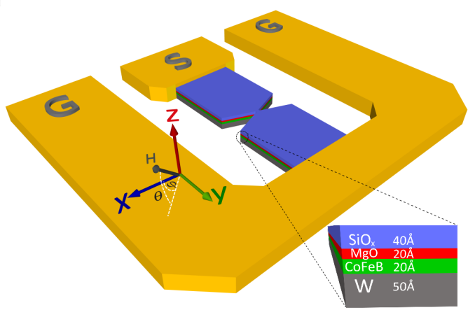
Figure 1 shows a schematic of the SHNO device including the CPW. The inset shows the magnified view of the constituent layers and their thicknesses. A positive direct current is defined to flow from the signal pad to ground in the -direction. and are the in-plane (IP) and out-of-plane (OOP) field angles, respectively.

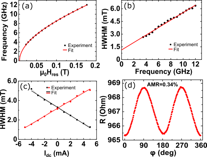
We first investigated the magnetodynamic properties of the stack using ST-FMR measurement on a 6 18 bar by applying a direct current (dc) and a 98.76 Hz modulated microwave current through the input port of a bias-tee at a fix rf frequency, and detecting the resulting voltage on its output port using a lock-in amplifier while sweeping the magnetic field (0–0.2 T). The voltage response from each sweep was fit to a sum of one symmetric and one antisymmetric Lorentzian sharing the same resonance field and linewidth.Liu et al. (2011) Figure 2(a) shows the resonance fields extracted at different microwave frequencies (3–12 GHz) without any direct current. The field dependence is well described by a Kittel behaviorKittel (1948) with an effective magnetization of = 0.71 T and a gyromagnetic ratio of = 30.9 GHz/T. It is interesting to compare = 0.71 T with 1.17 T measured using Alternating Gradient Magnetometry (AGM). According to equation . , the significantly lower indicates a moderate perpendicular magnetic anisotropy (PMA) field of 0.46 T.Liu et al. (2011); Peng et al. (2015)
Figure 2(b) shows the extracted linewidth for the same set of sweeps along with a linear fit Kittel (1948) yielding a low Gilbert damping of = 1.36 10-2. Figure 2(c) shows the current-induced linewidth changes of the ST-FMR spectra due to SOT, at a fixed frequency of 5 GHz. The linewidth has a linear current dependence with a negative (positive) slope for an IP field angle of = 30∘ ( = 210∘) from which we can extract -0.53, which is the highest reported for W.Demasius et al. (2016); Mondal et al. (2017); Zhang et al. (2016) Figure 2(d) shows an anisotropic magnetoresistance of 0.34 for a 120 nm wide nano-constriction. This is about an order of magnitude larger than the previously reported value of 0.026 for CoFeB Ranjbar et al. (2014) and relates to the fact that our annealing step turns the initially amorphous Co20Fe60B20 into a more poly-crystalline microstructure.

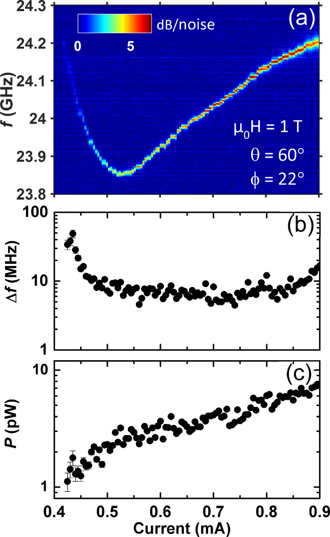
To investigate auto-oscillations, the lock-in amplifier was replaced with a low noise +43 dB amplifier and a spectrum analyzer, and the generated microwave power spectral density (PSD) was recorded as a function of direct current and applied magnetic field. Figure 3(a) shows the current dependent PSD from a = 120 nm nano-constriction measured in a constant 1 T field with = 22∘ and = 60∘. The non-monotonic current dependence—first red-shifted, then blue-shifted—is typical for a nano-constriction SHNO in a close-to-perpendicular magnetic field.Dvornik, Awad, and Åkerman (2018); Awad et al. (2016) The auto-oscillation region starts at the constriction edge (red-shift) and, as the current increases, moves to the center and expands to fill the constriction region (blue-shift)Awad et al. (2016). The linewidth (Figure 3(b)) and integrated power (Figure 3(c)) were obtained by Lorentzian fits to the PSD; the linewidth decreases and the power increases with increasing current. The maximum integrated power of about 8 pW has been achieved at low operational current of 0.9 mA which is considerably higher compared to previous reports on NiFe/Pt Awad et al. (2016); Dürrenfeld et al. (2017) and NiFe/W Mazraati et al. (2016) SHNOs. The high reduces the auto-oscillation threshold current to about = 0.5 mA (determined as in Ref. [(32)]), corresponding to a 4.4 107 A/cm2 current density in the W layer, i.e. very close to previously reported values for NiFe/W SHNOs in in-plane fieldsMazraati et al. (2016). Reducing the field magnitude to 0.8 T, we extracted an even lower threshold of about 3.3 107 A/cm2. It may be pointed out that wider nano-constriction width offers an increased auto-oscillation mode volume which in turn reduces the line-width of auto-oscillation peaks and enhances the peak power. However, lateral confinement of the nano-constriction, within the limit of reasonable yield of SHNO devices, results into a linear rise in resistance and an equivalent decrease in threshold current, thereby reduces the power consumption via quadratic dependence on current. Therefore, an optimum nano-constriction width of 120 nm has been chosen in this present work to efficiently realize the conducive operational characteristics with lesser power consumption.

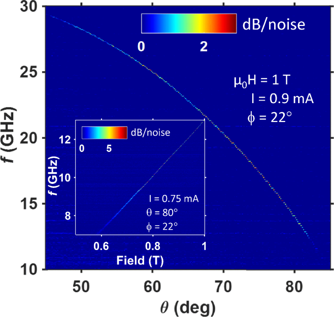
To examine the operational frequency range of our SHNOs, we investigated their auto-oscillations as a function of OOP angle at a fixed field magnitude ( = 1 T) and current ( 0.9 mA). Figure 4 displays the resulting auto-oscillations, which range from 12 to 28 GHz. As the OOP angle increases, the IP component of the magnetic field becomes smaller in magnitude and therefore shifts both the FMR frequency and the auto-oscillation operating frequency to lower values. It can be noted that our SHNOs are operative in a wide frequency range from 12 GHz up to 28 GHz by just tailoring the OOP angle. The inset in Figure 4 further shows the field dependence of auto-oscillation frequency at a fixed OOP angle ( = 80∘) and dc-current (=0.75 mA). The variation in the magnitude of external magnetic field gives rise to the tilting of internal magnetization angle with respect to IP direction which is manifested as a linear rise of the precessional frequency from 7 GHz up to 13 GHz. It is noteworthy that an observable auto-oscillation signal clearly persists down to much lower field values than that suggested by , which emphasizes the beneficial role of the moderate PMA in extending the field range. As a potential route to further reduce the required magnetic field to levels where integrated thin film permanent magnets would be sufficient, one could increase the PMA by thinning the CoFeB.
In conclusion, we have demonstrated CMOS compatible nano-constriction SHNOs based on W/Co20Fe60B20/MgO stacks grown on highly resistive Si substrates. Thanks to the record high spin Hall angle of the W layer ( = -0.53) and the moderate perpendicular magnetic anisotropy of the Co20Fe60B20 layer, these SHNOs exhibit very low threshold currents and operate over a very wide frequency range, 7–28 GHz. Also, such devices could be further integrated on Si with other microwave components to offer more compact and tunable microwave devices used in RF CMOS communication systems.
This work was supported by the Swedish Foundation for Strategic Research (SSF), the Swedish Research Council (VR), and the Knut and Alice Wallenberg foundation (KAW). This work was also supported by the European Research Council (ERC) under the European Community’s Seventh Framework Programme (FP/2007-2013)/ERC Grant 307144 “MUSTANG”.
I References
References
- Hirsch (1999) J. E. Hirsch, Phys. Rev. Lett. 83, 1834–1837 (1999).
- Sinova et al. (2015) J. Sinova, S. O. Valenzuela, J. Wunderlich, C. H. Back, and T. Jungwirth, Rev. Mod. Phys. 87, 1213–1260 (2015).
- Liu et al. (2012a) L. Liu, C.-F. Pai, Y. Li, H. Tseng, D. Ralph, and R. Buhrman, Science 336, 555–558 (2012a).
- Liu et al. (2012b) L. Liu, C.-F. Pai, D. C. Ralph, and R. A. Buhrman, Phys. Rev. Lett. 109, 186602 (2012b).
- Awad et al. (2016) A. Awad, P. Dürrenfeld, A. Houshang, M. Dvornik, E. Iacocca, R. Dumas, and J. Åkerman, Nature Physics , 292––299 (2016).
- Mazraati et al. (2016) H. Mazraati, S. Chung, A. Houshang, M. Dvornik, L. Piazza, F. Qejvanaj, S. Jiang, T. Q. Le, J. Weissenrieder, and J. Åkerman, Applied Physics Letters 109, 242402 (2016).
- Dürrenfeld et al. (2017) P. Dürrenfeld, A. A. Awad, A. Houshang, R. K. Dumas, and J. Åkerman, Nanoscale 9, 1285–1291 (2017).
- Chen et al. (2016) T. Chen, R. K. Dumas, A. Eklund, P. K. Muduli, A. Houshang, A. A. Awad, Dürrenfeld, B. G. Malm, A. Rusu, and J. Åkerman, Proceedings of the IEEE 104, 1919–1945 (2016).
- Demidov et al. (2012) V. E. Demidov, S. Urazhdin, H. Ulrichs, V. Tiberkevich, A. Slavin, D. Baither, G. Schmitz, and S. O. Demokritov, Nature Mater. 11, 1028–1031 (2012).
- Demidov et al. (2014) V. E. Demidov, S. Urazhdin, A. Zholud, A. V. Sadovnikov, and S. O. Demokritov, Appl. Phys. Lett. 105, 172410 (2014).
- Ranjbar et al. (2014) M. Ranjbar, P. Dürrenfeld, M. Haidar, E. Iacocca, M. Balinskiy, T. Q. Le, M. Fazlali, A. Houshang, A. A. Awad, R. K. Dumas, and J. Åkerman, IEEE Magnetics Letters 5, 3000504 (2014).
- Collet et al. (2016) M. Collet, X. de Milly, O. d’Allivy Kelly, V. V. Naletov, R. Bernard, P. Bortolotti, J. Ben Youssef, V. E. Demidov, S. O. Demokritov, J. L. Prieto, M. Munoz, V. Cros, A. Anane, G. de Loubens, and O. Klein, Nat. Commun. 7, 10377 (2016).
- Laczkowski et al. (2017) P. Laczkowski, Y. Fu, H. Yang, J.-C. Rojas-Sánchez, P. Noel, V. Pham, G. Zahnd, C. Deranlot, S. Collin, C. Bouard, et al., arXiv preprint arXiv:1708.09214 (2017).
- Niimi et al. (2012) Y. Niimi, Y. Kawanishi, D. H. Wei, C. Deranlot, H. X. Yang, M. Chshiev, T. Valet, A. Fert, and Y. Otani, Phys. Rev. Lett. 109, 156602 (2012).
- Reyes et al. (1996) A. C. Reyes, S. M. El-Ghazaly, S. Dorn, M. Dydyk, D. K. Schroder, and H. Patterson, in Electronic Components and Technology Conference, 1996. Proceedings., 46th (IEEE, 1996) pp. 382–391.
- Cohen et al. (1982) S. Cohen, P. Piacente, G. Gildenblat, and D. Brown, Journal of Applied Physics 53, 8856–8862 (1982).
- Murarka (1995) S. P. Murarka, Intermetallics 3, 173–186 (1995).
- Luo et al. (2010) J. Luo, Z. Qiu, C. Zha, Z. Zhang, D. Wu, J. Lu, J. Åkerman, M. Östling, L. Hultman, and S.-L. Zhang, Applied Physics Letters 96, 031911 (2010).
- Siegal, Graham, and Santiago (1989) M. Siegal, W. Graham, and J. Santiago, Journal of Applied Physics 66, 6073–6076 (1989).
- Doris et al. (2016) B. Doris, B. DeSalvo, K. Cheng, P. Morin, and M. Vinet, Solid-State Electronics 117, 37–59 (2016).
- Shahidi (2002) G. G. Shahidi, IBM journal of Research and Development 46, 121–131 (2002).
- Zhang et al. (2016) C. Zhang, S. Fukami, K. Watanabe, A. Ohkawara, S. DuttaGupta, H. Sato, F. Matsukura, and H. Ohno, Applied Physics Letters 109, 192405 (2016).
- Lee, Shim, and Park (2016) S.-E. Lee, T.-H. Shim, and J.-G. Park, NPG Asia Materials 8, e324 (2016).
- Mondal et al. (2017) S. Mondal, S. Choudhury, N. Jha, A. Ganguly, J. Sinha, and A. Barman, Physical Review B 96, 054414 (2017).
- Demasius et al. (2016) K.-U. Demasius, T. Phung, W. Zhang, B. P. Hughes, S.-H. Yang, A. Kellock, W. Han, A. Pushp, and S. S. P. Parkin, Nat. Commun. 7, 10644 (2016).
- Pai et al. (2012) C.-F. Pai, L. Liu, Y. Li, H. Tseng, D. Ralph, and R. Buhrman, Applied Physics Letters 101, 122404 (2012).
- Liu et al. (2011) L. Liu, T. Moriyama, D. C. Ralph, and R. A. Buhrman, Phys. Rev. Lett. 106, 036601 (2011).
- Kittel (1948) C. Kittel, Phys. Rev. 73, 155 (1948).
- Liu et al. (2011) X. Liu, W. Zhang, M. J. Carter, and G. Xiao, Journal of Applied Physics 110, 033910 (2011).
- Peng et al. (2015) S. Peng, M. Wang, H. Yang, L. Zeng, J. Nan, J. Zhou, Y. Zhang, A. Hallal, M. Chshiev, K. L. Wang, et al., Scientific reports 5, 18173 (2015).
- Dvornik, Awad, and Åkerman (2018) M. Dvornik, A. A. Awad, and J. Åkerman, Phys. Rev. Applied 9, 014017 (2018).
- Tiberkevich, Slavin, and Kim (2007) V. Tiberkevich, A. Slavin, and J.-V. Kim, Appl. Phys. Lett. 91, 192506 (2007).