Tailoring a nanofiber for enhanced photon emission and coupling efficiency from single quantum emitters
Abstract
We present a novel approach to enhance the spontaneous emission rate of single quantum emitters in an optical nanofiber-based cavity by introducing a narrow air-filled groove into the cavity. Our results show that the Purcell factor for single quantum emitters located inside the groove of the nanofiber-based cavity can be at least six times greater than that for such an emitter on the fiber surface when using an optimized cavity mode and groove width. Moreover, the coupling efficiency of single quantum emitters into the guided mode of this nanofiber-based cavity can reach up to 80 with only 35 cavity-grating periods. This new system has the potential to act as an all-fiber platform to realize efficient coupling of photons from single emitters into an optical fiber for quantum information applications.
pacs:
Valid PACS appear hereMicro- and nanoscale optical systems are receiving increasing attention from the quantum optics community. Owing to their capacity to create an efficient, scalable interface between light and matter at the single photon and single emitter levels, microscale systems are of fundamental importance for quantum information science 1 ; 2 ; 3 ; 4 . These systems should have an ultra-small mode volume to increase the spontaneous emission rate of single quantum emitters and should be able to couple fluorescent photons to a single mode fiber with high efficiency. In recent years, optical nanofibers (ONFs) with sub-wavelength diameters have attracted great interest from researchers as useful light-matter interface platforms 5 ; 6 benefiting from the tight confinement of the evanescent field around the fiber, the unique geometries provided by fiber modes, and low optical loss 7 ; 8 . They allow for the efficient coupling of fluorescent photons emitted by single emitters near the ONF surface to a propagating mode of the nanofiber and subsequently to the guided mode of a standard single-mode fiber through an adiabatically tapered region. Efficient coupling of photons from a variety of quantum emitters, such as laser-cooled atoms, has been experimentally demonstrated 9 ; 10 ; 11 ; 12 ; 13 ; 14 . As theoretically expected, about 8 of the guided light can be absorbed when an atom is trapped about 200 nm away from the nanofiber surface and this decreases gradually with increasing atom-surface distance 11 ; 15 ; 16 . For solid-state-based quantum emitters 17 , such as semiconductor quantum dots 18 ; 19 , nitrogen-vacancy (NV) centers in diamond 20 ; 21 ; 22 and even emitters in 2D materials 23 , experimental progress has demonstrated efficient positioning of such single quantum emitters onto the surface of a nanofiber. For single emitters located on a nanofiber surface, 20 of the fluorescent photons can be coupled into the fiber’s guided modes 19 . Various proposals for solid-state-based emitters based on optical nanofibers have been made with the aim of improving the coupling efficiency 24 ; 25 ; 26 ; 27 ; 28 ; 29 , especially ideas using nanofiber-based cavities 30 ; 31 . With the aid of such cavities, the coupling efficiency and the spontaneous emission rate of single-quantum emitters can be further increased because of the enhanced interaction of the emitter with its environment (Purcell effect) 32 . It has been predicted that the coupling efficiency could be close to unity by using nanofiber-based cavities 30 . Therefore, nanofiber-based cavity systems combined with ONFs and fiber in-line cavities have been proposed and fabricated utilizing various technologies 33 ; 34 ; 35 ; 36 ; 37 ; 38 . In addition, an enhancement of the spontaneous emission rate of single quantum dots based on such a system has been experimentally demonstrated 39 ; 40 . The aforementioned systems are for emitters located on the surfaces of nanofibers; however, further improvement of the interactions between emitters and guided modes are mostly modest for silica nanofibers. Thus, it is still challenging to achieve a significant enhancement of the fluorescence from single emitters coupled to fiber-based cavities with a high quality factor, Q , and a small effective mode volume, , as well as a high coupling efficiency.
In this Letter, we propose a tailored optical nanofiber (TONF) for enhanced photon emission and coupling efficiency from single-quantum emitters. This tailored nanofiber is a nanofiber-based cavity 41 with a narrow, air-filled groove inside the cavity (Fig. 1). In contrast to a simple slotted ONF for atom trapping 42 , introducing this groove not only allows for single emitters to reside in the strongest intensity field of the nanofiber, but it also induces an increase in the normalized maximum electric field, which significantly enhances the spontaneous emission rate of single emitters inside the cavity. For the TONF with a moderate groove width of 50 nm, the coupling efficiency for single emitters can reach 80 with a short-period number of air-nanohole arrays on the nanofiber and the Purcell factor can be as high as 90 . The dielectric discontinuities inside the cavity induced by this narrow air-filled groove can result in a 10 increase in the Purcell factor compared with the value on the cavity surface. These results pave the way for future experiments exploiting the Purcell-enhanced interaction between single emitters and the optical nanofiber-based cavity with a high coupling efficiency.
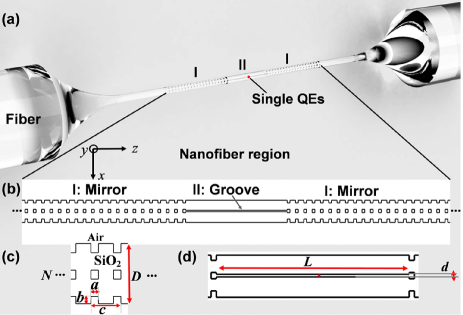
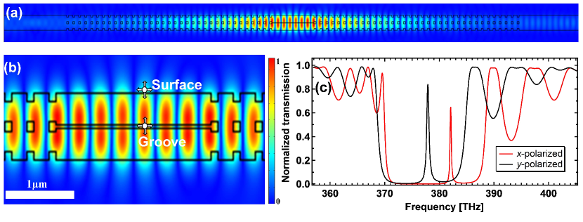
The TONF system shown in Fig.1 consists of two main parts: an optical nanofiber-based cavity induced by periodic air-nanohole arrays (structure I) and an air-filled groove embedded in the cavity region (structure II). Hence, the optical characteristics of this proposed structure are determined by both structures. We previously fabricated an optical nanofiber-based cavity induced by periodic air-nanohole arrays 41 with a high Q factor with very few grating periods. We used the same parameters for structure I as in our previous work (Fig. 1). When a narrow air-filled groove is introduced into the cavity region, the electric field distribution along the nanofiber for a polarized input mode is displayed in Fig. 2(a), obtained using a finite element method (FEM) based on COMSOL Multiphysics. An enlarged region of the groove is shown in Fig. 2(b) for two different cases, i.e. single emitters on the surface and in the groove. It shows the cross-sections of the normalized electric field distribution along the fiber (axial direction) for y- polarized modes with a nanofiber diameter of 800 nm and a groove width of 50 nm. The optical response spectrum, such as the transmission through the TONF, has been calculated by using a commercial finite-difference time-domain (FDTD) method performed on a commercial package (FDTD Solutions, Lumerical); see Fig. 2(c). Based on the resonant peaks for =35, the Q factors of the x- and y-polarized modes are 1578 and 796, respectively.
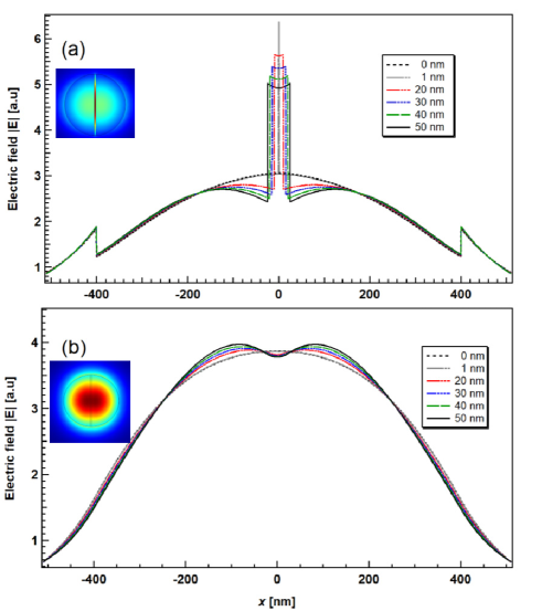
The air-filled groove embedded in the TONF induces local field enhancement in the normalized maximum field using dielectric discontinuities with subwavelength scales43 . From Maxwell’s equations, normal components of the electric displacement are continuous across the boundary of two different dielectrics, that is 44 . The intensity of the electric field distribution of the quasi x- and y-polarized modes in the TONF for different groove widths, , is shown in Fig. 3. The peak of the electric field for x- polarized modes at the cavity is enhanced 2x compared to the case without a groove inside the cavity (Fig. 3(a)). From Fig. 3 (b), for y- polarized modes, there is no significant distinction between the electric field distribution in the cavity with and without a groove. Compared to the value of the electric field on a fiber surface, the electric field in the groove increases many fold for both the x- and y-polarized modes.
The spontaneous decay rate of a quantum emitter can be enhanced when it is coupled to a TONF based on the Purcell effect (see Figure 1(a)), which was first described by E. M. Purcell in 1946 32 . In a TONF, i.e., a nanofiber-based cavity for which the resonant wavelength of the quantum emitter is tuned to the wavelength of the guided mode, the Purcell factor, F, is given in terms of the cavity quality factor, Q, and the effective mode volume , such that for an emitter located at the peak of the electric field with the index of refraction . Based on Fermi’s golden rule, modification of the spontaneous decay rates of single emitters is proportional to the number of local density of states (LDOS) of available final photon states. The LDOS for the electromagnetic modes is directly proportional to the imaginary part of the corresponding electromagnetic Green’s function. The spontaneous decay rate of a quantum emitter in the presence of the TONF can be given by 45 ,
| (1) |
where is the transition angular frequency, is the transition dipole moment, is the dipole moment of an emitter with being the unit vector in the direction of , and is the dyadic Green’s function calculated at the emitter’s location . To characterize the coupling between guided modes and a quantum emitter placed in the groove, the coupling efficiency is defined as the ratio between the emission from single emitters into the guided mode of a TONF and the total decay rate into all radiative channels in the presence of the TONF. Moreover, the emission enhancement factor can be written as with being the intrinsic spontaneous emission rate into free space. Therefore the total enhancement of the spontaneous emission from a single quantum emitter, namely, the Purcell factor, can be deduced as . Using the 3D finite-different time-domain (FDTD) method, the spontaneous decay rate and coupling efficiency can be obtained by calculating the Green’s tensor and the power emission into cavity modes.
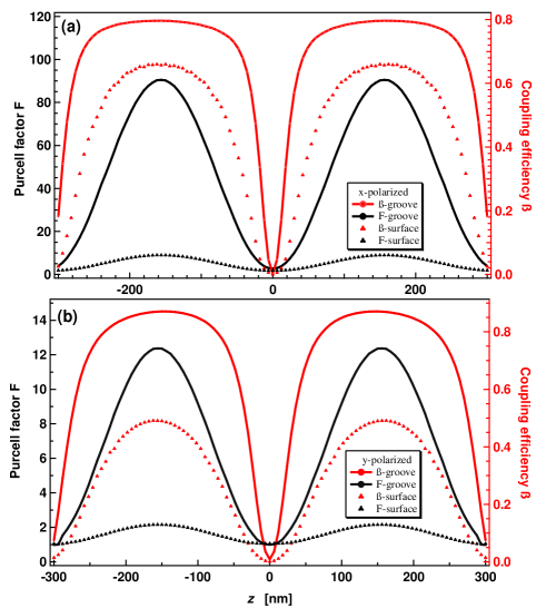
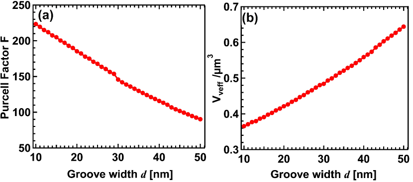
Figure 4 characterizes the coupling efficiency (solid red line) from single QEs and the corresponding Purcell factor F (solid black line) for an emitter positioned at the center of the groove along the z-axis. For comparison, the red- and black triangles in Fig .4(a) (b) represent the corresponding cases for an emitter on the surface of the nanofiber. With a groove of width =50 nm and a period number of 35, the Purcell factor F can reach 90 for x- polarized modes when an emitter is positioned at the peak intensity of the field in the groove; this is several times larger than that of the y- polarized modes owing to the field enhancement induced by the narrow air-filled groove. Compared with an emitter on the surface of the TONF, the Purcell factor F for both of the polarized modes increases by at least 6. The coupling efficiency of both polarized modes with the groove can reach 80, which is larger than that for the emitter on the surface of the TONF.
In principle, the air-filled groove width should be as small as possible to achieve the highest possible local field enhancement for x- polarized modes. Fig. 5 shows the change in the Purcell factor F and the effective mode volume with changes in the groove width , respectively. As expected, F gradually increases with decreasing width . In particular, F can reach as much as 220 with = 10 nm. To get as small an effective volume as possible, the width should be as small as possible. It shows that the effective mode volume can be further reduced by half when the width diminishes to zero. However, considering the practical size of an emitter such as a quantum dot, with a diameter of 6 nm, and the technical limitations on positioning it within the groove during an experiment, we choose =50 nm for the aforementioned calculation.
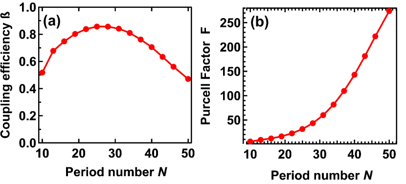
For further optimization of and F, we calculated their dependence on the period number ( Fig. 6). F increases with the increasing period number and F can reach 250 at =50. Additionally, the coupling efficiency presents a trend from rising to declining with increased period numbers due to the increased grating loss 31 which could be reduced by designing a modulated Bragg mirror 46 . Consequently, there is a tradeoff between the possible enhanced spontaneous decay rate of a quantum emitter denoted by F, and the possibility of coupling fluorescence photons from single emitters to the TONF, measured by the coupling efficiency . The efficiency reaches a maximum value for approximately 30 periods.
In summary, we have explored a tailored optical nanofiber (TONF) as a nanoscale cavity QED system that could yield a high photon collection efficiency of 80 and an enhancement of the spontaneous radiation decay rate for a single quantum emitter of F 90 using a moderate groove width of 50 nm. We have shown that the TONF with the narrow air-filled groove is a useful system for efficient coupling of fluorescence photons from single emitters into an optical fiber and should provide enhanced interaction between single quantum emitters and the guided mode of a nanofiber. This system could be used for observing strong light-matter interactions and multicolor quantum manipulation such as atom trapping for quantum information processing.
This work was supported by Okinawa Institute of Science and Technology Graduate University.The authors would like to thank F. Le Kien for invaluable discussions. S.Aird are acknowledged for comments on the manuscript.
References
- (1) H. J. Kimble, Nature (London) 453, 1023 (2008).
- (2) D. E. Chang, V. Vuletić, and M. D. Lukin, Nature Photon. 8, 685 (2014).
- (3) P. Lodahl, S. Mahmoodian, and S. Stobbe, Rev. Mod. Phys. 87, 347 (2015).
- (4) A. Reiserer, and G. Rempe, Rev. Mod. Phys. 87, 1379 (2015).
- (5) T. Nieddu , V. Gokhroo , and S. Nic Chormaic , J. Opt. 18, 053001 (2016).
- (6) P. Solano, J. A. Grover, J. E. Hoffman, S. Ravets, F. K. Fatemi, L. A. Orozco, and S. L. Rolston, Adv. At. 66, 439 (2017).
- (7) X. Q. Wu and L. M. Tong, Nanophotonics 2, 407 (2013).
- (8) J. M. Ward, A. Maimaiti, Vu H. Le, and S. Nic Chormaic, Rev. Sci. Instrum. 85, 111501(2014).
- (9) G. Sagué, E. Vetsch, W. Alt, D. Meschede, and A. Rauschenbeutel, Phys. Rev. Lett. 99, 163602 (2007).
- (10) K. P. Nayak, P. N. Melentiev, M. Morinaga, F. Le Kien,V. I. Balykin, and K. Hakuta, Opt. Express 15, 5431 (2007).
- (11) A. Goban, K. S. Choi, D. J. Alton, D. Ding, C. Lacroute, M.Pototschnig, T. Thiele, N. P. Stern, and H. J. Kimble, Phys.Rev. Lett. 109, 033603 (2012).
- (12) B. Gouraud, D. Maxein, A. Nicolas, O. Morin, and J. Laurat Phys. Rev. Lett. 114, 180503 (2015).
- (13) H. L. Sørensen, J. B. Beguin, K. W. Kluge, I. Iakoupov, A. S. Sørensen, J. H. Muller, E. S. Polzik, and J. Appel, Phys. Rev. Lett. 117, 133604 (2016).
- (14) R. Kumar, V. Gokhroo, K. Deasy, and S. Nic Chormaic, Phys. Rev. A 91,053842 (2015).
- (15) E. Vetsch, D. Reitz, G. Sagué, R. Schmidt, S. T. Dawkins, and A. Rauschenbeutel, Phys. Rev. Lett. 104, 203603 (2010).
- (16) F. Le Kien, S. Dutta Gupta, V. I. Balykin, and K. Hakuta, Phys. Rev. A 72, 032509 (2005).
- (17) I. Aharonovich, D. Englund, and M. Toth, Nat. Photonics 10, 631 (2016).
- (18) M. Fujiwara, K. Toubaru, T. Noda, H. Q. Zhao, and S.Takeuchi, Nano Lett. 11, 4362 (2011).
- (19) R. Yalla, F. Le Kien, M. Morinaga, and K. Hakuta, Phys.Rev. Lett. 109, 063602 (2012).
- (20) L. Liebermeister, F. Petersen, A. V. Munchow, D. Burchardt, J. Hermelbracht, T. Tashima, A. W. Schell, O. Benson, T.Meinhardt, A. Krueger, A. Stiebeiner, A. Rauschenbeutel, H. Weinfurter, and M. Weber, Appl. Phys. Lett. 104, 031101 (2014).
- (21) M. Fujiwara, H.-Q. Zhao, T. Noda, K. Ikeda, H. Sumiya, and S. Takeuchi, Opt. Lett. 40(24), 5702 (2015).
- (22) V. V. Vorobyov, V. V. Soshenko, S. V. Bolshedvorskii, J. Javadzade, N. Lebedev, A. N. Smolyaninov, V. N. Sorokin, and A. V. Akimov, Eur. Phys. J. D 70(12), 269 (2016).
- (23) A. W. Schell, H. Takashima, T. T. Tran, I. Aharonovich,and S. Takeuchi, ACS Photonics 4, 761 (2017).
- (24) M. Davanço and K. Srinivasan, Opt. Express 17, 10542 (2009).
- (25) R. Albrecht, Al. Bommer, C. Deutsch, J. Reichel, and C. Becher, Phys. Rev. Lett. 110, 243602 (2013).
- (26) S. Chonan, S. Kato, and T. Aoki, Sci Rep 4, 4785(2014).
- (27) T. G. Tiecke, K. P. Nayak, J. D. Thompson, T. Peyronel, N. P. de Leon, V. Vuletić, and M. D. Lukin, Optica 2, 70 (2015).
- (28) R. N. Patel, T. Schröder, N. Wan, L. Li, S. L. Mouradian, E. H. Chen, and D. R. Englund, Light Sci. Appl. 5,e16032 (2016).
- (29) Y. Yonezu, K. Wakui, K. Furusawa, M. Takeoka, K. Semba, and T. Aoki, Sci Rep 7, 12985 (2017).
- (30) F. Le Kien and K. Hakuta, Phys. Rev. A 80, 053826 (2009).
- (31) H. Takashima, M. Fujiwara, A. W. Schell, and S. Takeuchi, Opt. Express, 24, 15050 (2016).
- (32) E. M. Purcell, Phys. Rev. 69, 681 (1946).
- (33) K. P. Nayak, F. Le Kien, Y. Kawai, K. Hakuta, K. Nakajima, H. T. Miyazaki, and Y. Sugimoto, Opt. Express 19, 14040 (2011).
- (34) M. Sadgrove, R. Yalla, K. P. Nayak, and K. Hakuta, Opt. Lett. 38, 2542(2013).
- (35) C. Wuttke, M. Becker, S. Brückner, M. Rothhardt, and A. Rauschenbeutel, Opt. Lett. 37, 1949 (2012).
- (36) K. P. Nayak, P. Zhang, and K. Hakuta, Opt. Lett. 39, 232(2014).
- (37) D. E. Jones, G. T. Hickman, J. D. Franson, and T. B. Pittman, Opt. Lett. 41, 3683 (2016).
- (38) Y. Sun, Y. Yu, H. Liu, Z. Li, and W. Ding, J. Phys.: Conf. Ser. 680,012029 (2016).
- (39) R. Yalla, M. Sadgrove, K. P. Nayak, and K. Hakuta, Phys. Rev. Lett. 113,143601 (2014).
- (40) A. W. Schell, H. Takashima, S. Kamioka, Y. Oe, M. Fujiwara, O. Benson, and S. Takeuchi, Sci. Rep. 5, 9619 (2015).
- (41) W. Li, J. Du, V. G. Truong and S. Nic Chormaic, Appl. Phys. Lett. 110, 253102 (2017).
- (42) M. Daly, V. G. Truong, C. Phelan, K. Deasy, and S. Nic Chormaic, New J. Phys. 16, 053052 (2014).
- (43) V. R. Almeida, Q. Xu, C. A. Barrios, and M. Lipson, Opt.Lett. 29, 1209 (2004).
- (44) J. T. Robinson, C. Manolatou, L. Chen, M. Lipson, Phys. Rev. Lett. 95, 143901 (2005).
- (45) L. Novotny and B. Hecht. Principle of Nano-optics.2006.
- (46) Q. Quan,P. B. Deotare, and M. Loncar, Appl. Phys. Lett. 96, 203102 (2010).