Phonon transport of Janus monolayer MoSSe: a first-principles study
Abstract
Transition Metal Dichalcogenide (TMD) monolayers have most widely studied due to their unique physical properties. Recently, Janus TMD Monolayer MoSSe with sandwiched S-Mo-Se structure has been synthesized by replacing the top S atomic layer in with Se atoms. In this work, we systematically investigate the phonon transport and lattice thermal conductivity () of MoSSe monolayer by first-principles calculations and linearized phonon Boltzmann equation within the single-mode relaxation time approximation (RTA). Calculated results show that the of MoSSe monolayer is very lower than that of monolayer, and higher than that of monolayer. The corresponding sheet thermal conductance of MoSSe monolayer is 342.50 at room temperature. These can be understood by phonon group velocities and lifetimes. Compared with monolayer, the smaller group velocities and shorter phonon lifetimes of MoSSe monolayer give rise to lower . The larger group velocities for MoSSe than monolayer is main reason of higher . The elastic properties of , MoSSe and monolayers are also calculated, and the order of Young’s modulus is identical with that of . Calculated results show that isotope scattering leads to 5.8% reduce of . The size effects on the are also considered, which is usually used in the device implementation. When the characteristic length of MoSSe monolayer is about 110 nm, the reduces to half. These results may offer perspectives on thermal management of MoSSe monolayer for applications of thermoelectrics, thermal circuits and nanoelectronics, and motivate further theoretical or experimental efforts to investigate thermal transports of Janus TMD monolayers.
pacs:
72.15.Jf, 71.20.-b, 71.70.Ej, 79.10.-n Email:sandongyuwang@163.comI Introduction
Due to many novel properties, two-dimensional (2D) materials have been attracting increasing attention since the discovery of grapheneq1 . The TMDq7 , group-VAq9 ; q10 , group IV-VIq8 and group-IVq11 monolayers have been predicted theoretically or synthesized experimentally, which have potential applications in electronic, thermoelectric, quantum and optoelectronic devices. Recently, Janus monolayer MoSSe has been synthesized, based on monolayer by breaking the out-of-plane structural symmetryp1 . The existence of vertical dipoles has been proved by second harmonic generation and piezoresponse force microscopy measurementsp1 . The strong piezoelectric effects have been predicted in monolayer and multilayer Janus TMD MXY (M = Mo and W; X/Y = S, Se and Te) by first-principles calculationsp2 , which has potential applications in energy harvesting and sensors. Electronic and optical properties have been studied in pristine Janus MoSSe and WSSe monolayers and their vertical and lateral heterostructuresp3 . The ZrSSe monolayer has also been predicted with the 1T phasep4 , which is different from MoSSe monolayer with 2H phase. It is proved that ZrSSe monolayer has better n-type thermoelectric properties than monolayer .

The thermal property of 2D materials is quite worth studying due to its importance on the performance and reliability on the nano-devices. As is well known, a high thermal conductivity can effectively remove the accumulated heat, while a low thermal conductivity is beneficial to thermoelectric applications. In theory, thermal transports of many 2D materials have been widely studiedp5 ; q21 ; q22 ; l1 ; l2 ; l4 ; l4-1 ; l4-2 ; l4-3 ; l7 ; l71 ; l8 ; l9 ; l10 ; l102 ; l100 ; l101 , such as TMD, group-VA, ATeI (A=Sb or Bi), group IV-VI and group-IV monolayers. It is found that strain can effectively tune for various kinds of 2D materials, such as group-IV monolayersl9 ; l101 ; l100 , l4-3 , antimonenel102 and Penta-Structures monolayersl10 . With strain increasing, the shows monotonous increase/decrease and up-and-down behavior, and tensile strain can induce strong size effects on . The phonon transports of TMD (M=Mo, W, Zr and Hf; X=S and Se) monolayers have been systematically studied by phonon Boltzmann transport equation approachp5 . The of 2H-type TMD monolayers are generally higher than those of 1T-type ones, which can be attributed to the large acoustic-optical frequency gapp5 . In this work, the phonon transport of Janus TMD MoSSe monolayer is performed from a combination of first-principles calculations and linearized phonon Boltzmann equation. It is found that the of MoSSe monolayer is very lower than that of monolayer, but higher than one of monolayer. The order of their is explored by phonon group velocities and lifetimes. It is found that the order of Young’s modulus ( MoSSe ) is identical with that of , which accords with the relation: q16 . The isotope and size effects on are also studied, which can provide valuable information for designing MoSSe-based nano-electronics devices.
The rest of the paper is organized as follows. In the next section, the computational details about phonon transport calculations are given. In the third section, the phonon transport and elastic properties of MoSSe monolayer, together with ones of and monolayers for a comparison, are shown. Finally, we shall give some discussions and conclusions in the fourth section.
| Name | ||||
|---|---|---|---|---|
| 3.18 (3.17p1 ) | 2.41 | - | 3.12 | |
| MoSSe | 3.25 (3.23p1 ) | 2.42 | 2.54 | 3.23 |
| 3.30 (3.30p1 ) | - | 2.54 | 3.35 |
| Name | ||||
|---|---|---|---|---|
| 8.29 (8.49p6 ) | 11.20 (11.55p6 ) | 11.91 (12.12p6 ) | 13.73 (14.10p6 ) | |
| MoSSe | 6.00 | 10.24 (10.65p1 ) | 8.50 (8.64p1 ) | 12.83 |
| 4.88 (5.01p7 ) | 8.35(8.46p7 ) | 7.06 (7.20p7 ) | 10.34 (10.53p7 ) |
II Computational detail
Within projector augmented-wave method, we perform the first-principles calculations using the VASP codepv1 ; pv2 ; pv3 ; pbe by adopting generalized gradient approximation of Perdew-Burke-Ernzerhof (PBE-GGA) as exchange-correlation functionalpbe . During structural relaxation, a 20 20 1 k-mesh is used with a Hellman-Feynman force convergence threshold of eV/ . A plane-wave basis set is employed with kinetic energy cutoff of 450 eV, and the electronic stopping criterion is eV. The 5s and 4d electrons of Mo, and 3/4s and 3/4p electrons of S/Se are treated as valance ones. The lattice thermal conductivity is performed by using Phono3py+VASP codespv1 ; pv2 ; pv3 ; pv4 . By solving linearized phonon Boltzmann equation, the is calculated with single-mode RTA, as implemented in the Phono3py codepv4 . The can be expressed as:
| (1) |
in which , and are phonon mode, the total number of q points sampling Brillouin zone (BZ) and the volume of a unit cell, and , , is the specific heat, phonon velocity, phonon lifetime. The phonon lifetime can be attained by phonon linewidth of the phonon mode :
| (2) |
The takes the form analogous to the Fermi golden rule:
| (3) |
in which and are the phonon equilibrium occupancy and the strength of interaction among the three phonons , , and involved in the scattering. Based on the supercell approach with finite atomic displacement of 0.03 , the second-order interatomic force constants (IFCs) can be attained by using a 5 5 1 supercell with k-point meshes of 2 2 1. According to second-order harmonic IFCs, phonon dispersions can be calculated by Phonopy packagepv5 . The third-order IFCs can be attained by using a 3 3 1 supercell with k-point meshes of 3 3 1. To compute accurately lattice thermal conductivity, the reciprocal spaces of the primitive cells are sampled by 100 100 1 meshes .
For 2D material, the calculated lattice thermal conductivity depends on the length of unit cell along z direction2dl . They should be normalized by multiplying , where and are the length of unit cell along z direction and the thickness of 2D material. However, the is not well defined, for example graphene. In this work, the =24.64 is used as . By , the thermal sheet conductance can be attained.
III MAIN CALCULATED RESULTS AND ANALYSIS
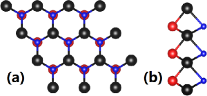
The structure of Janus MoSSe monolayer is similar to / monolayer with the 2H phase, containing three atomic sublayers with Mo layer sandwiched between S and Se layers. The Janus monolayer MoSSe can be constructed by replacing one of two S (Se) layers with Se (S) atoms in () monolayer. The schematic crystal structure of MoSSe monolayer is plotted in Figure 1. It is clearly seen that the Janus MoSSe monolayer loses the reflection symmetry with respect to the central metal Mo atoms compared with / monolayer. Therefore, the MoSSe monolayer (No.156) has lower symmetry compared with / monolayer (No.187). To avoid spurious interaction between neighboring layers, the unit cell of Janus MoSSe monolayer, containing one Mo, one S and one Se atoms, is constructed with the vacuum region of more than 18 . The optimized lattice constants (other theoretical valuesp1 ) and bond lengths of , MoSSe and monolayers are listed in Table 1. It is expected that of MoSSe monolayer is between ones of and monolayers, which is about 2.2% higher than that of monolayer, and 1.5% lower than that of monolayer. It is noted that the bond length of Mo-S/Se between MoSSe and monolayers is almost the same. The bond length of S-Se of MoSSe monolayer is between ones of S-S () and Se-Se ().
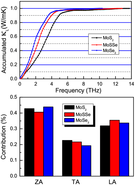
Figure 2 shows the phonon dispersions of , MoSSe and monolayers along high symmetry path, which agree well with previous resultsp1 ; p5 ; l4 . The 3 acoustic and 6 optical phonon branches are observed due to three atoms in the unit cell. The longitudinal acoustic (LA) and transversal acoustic (TA) branches are linear near the point, while out-of-plane acoustic (ZA) branch deviates from linearity. Similar behavior can be found in many 2D materialsq21 ; q22 ; l1 ; l2 ; l4 ; l7 ; l71 ; l8 ; l9 ; l10 ; l102 ; l100 ; l101 . Due to symmetry for , MoSSe and monolayers, the optical lattice-vibration modes at point can be defined as:
| (4) |
in which IR and R mean infrared- and Raman-active mode, respectively. The optical phonon frequencies of , MoSSe and monolayers at the point along with available experimental values are listed in Table 2. The calculated phonon frequencies of and monolayers are in agreement with the experimental resultsp1 ; p6 ; p7 . From to MoSSe to monolayer, acoustic modes become softened, and the optical branches overall move toward lower energy, which mean reduced group velocities. A frequency gap between the acoustic and optical phonon branches can be observed, which is due to mass differences between the constituent atomsm1-1 ; m3-1 . The frequency gap is 1.36 THz for , 0.63 THz for MoSSe and 0.15 THz for . The frequency gap along with the width of acoustic branches are listed in Table 3, which agree well with available theoretical resultsp5 ; l4 . It is noted that the frequency gap can produce important influence on acoustic+acousticoptical (aao) scatteringp5 . The large gap induces ineffective aao scattering due to the requirement on energy conservation, while small gap results in much more frequent aao scattering. These have important effects on phonon transports of both bulk and 2D materialsh5 ; h6 ; p5 .

| Name | |||
|---|---|---|---|
| 1.36 (1.35p5 ) | 6.93 (6.90p5 ,7.01l4 ) | 570.42 (509.84p5 ) | |
| MoSSe | 0.63 | 5.37 | 342.50 |
| 0.15 | 4.74 (4.73l4 ) | 284.35 (307.33p5 ) |
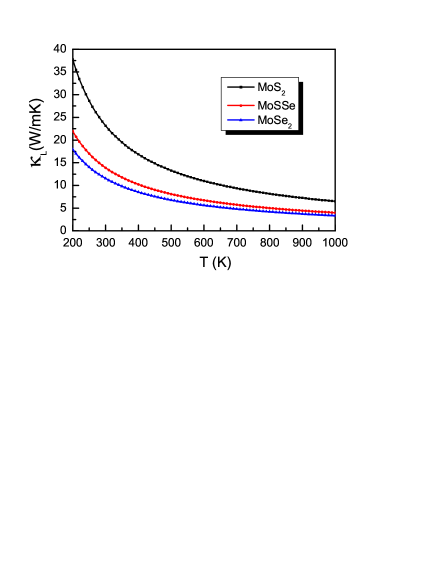
Within RTA method, Figure 3 shows the intrinsic lattice thermal conductivities of , MoSSe and monolayers from harmonic and anharmonic IFCs. With the same thickness (24.64 ), the room-temperature lattice thermal conductivity is 23.15 , 13.90 and 11.54 , respectively. Their thermal sheet conductance2dl is 570.42 , 342.50 and 284.35 , respectively. The thermal sheet conductances of , MoSSe and monolayers are listed in Table 3, together with reported theoretical valuesp5 using similar RTA method, which have been converted into thermal sheet conductances. Our calculated values of and monolayers are very close to previous onesp5 . It is expected that the lattice thermal conductivity of MoSSe monolayer is between ones of and monolayers. In the considered temperature range, the of MoSSe monolayer is about 60% of one of monolayer, and around 121% of of . For , MoSSe and monolayers, the ratio between accumulated and total lattice thermal conductivity with respect to frequency are plotted in Figure 4 at room temperature. It is clearly seen that acoustic branches of , MoSSe and monolayers dominate lattice thermal conductivity, providing a contribution of 97.3%, 97.6% and 96.9%, respectively. The relative contribution of every phonon mode of acoustic branches to the total lattice thermal conductivity (300 K) also are shown in Figure 4. It is found that the order of contribution is ZA LA TA for all three monolayers, and about 42% for ZA mode, 33% for TA mode and 21% for LA mode.
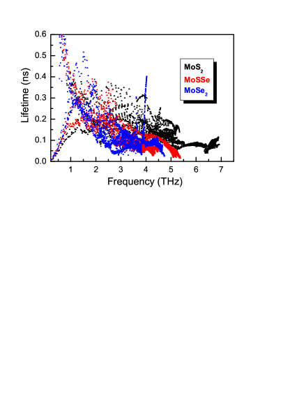
To further understand phonon transports of , MoSSe and monolayers, phonon mode group velocities and lifetimes are calculated. Due to dominant contribution to total from acoustic phonon branches, we only show acoustic phonon mode group velocities and lifetimes in Figure 5 and Figure 6. From to MoSSe to monolayer, most of group velocities become small due to softened acoustic phonon modes, which results in the decrease of the lattice thermal conductivity. The largest phonon group velocity at the point of the LA/TA modes decreases from 6.60/4.11 km/s to 5.62/3.55 km/s to 5.06/3.22 km/s from to MoSSe to monolayer. For ZA branch, the largest phonon group velocity changes from 4.18 km/s to 3.56 km/s to 3.29 km/s. Therefore, the group velocity reduction may be partial reason for the thermal conductivity reduction from to MoSSe to monolayer. It is straightforward to find that most of phonon lifetimes of MoSSe and monolayers are shorter than ones of monolayer, which may be due to larger acoustic and optical phonon gap. However, the phonon lifetimes between MoSSe and monolayers are comparative. The lower for MoSSe/ than monolayer is due to lower group velocities and shorter lifetimes. The of is lower than that of MoSSe, which is mainly due to lower group velocities.
| Name | |||||
|---|---|---|---|---|---|
| 131.7 (138.5p2 , 130p8 , 130.3p9 ) | 31.2 (31.7p2 , 32p8 , 31.0p9 ) | 50.3 | 124.3 | 0.24 | |
| MoSSe | 119.3 (126.8p2 ) | 27.5 (27.4p2 ) | 45.9 | 113.0 | 0.23 |
| 115.6 (115.9p2 , 108p8 , 110.1p9 ) | 26.5 (24.0p2 , 25p8 , 26.0p9 ) | 44.6 | 109.5 | 0.23 |
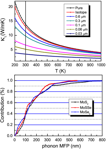
Based on the formula proposed by Shin-ichiro Tamuraq24 , phonon-isotope scattering is included, and the mass variance parameters are read from database of the natural abundance data for elements. The room temperature ”isotope effect” can be measured by . The calculated value is 6.2%, which means that phonon-isotope scattering has little effects on . With increasing temperature, isotopic effect on gradually becomes weak due to enhancement of phonon-phonon scattering. In reality, finite-size sample is usually used in the device implementation. By adopting a most simple boundary scattering model, the boundary scattering rate can be obtained by , in which , are the group velocity and boundary mean free path (MFP), respectively. The lattice thermal conductivities of infinite and finite-size (0.6, 0.3, 0.1, 0.06 and 0.03 ) MoSSe monolayer as a function of temperature are plotted in Figure 7. It is apparent that the thermal conductivity decreases with length decreasing, which is due to enhanced boundary scattering. For the 0.6, 0.3, 0.1, 0.06 and 0.03 cases, the room-temperature of MoSSe monolayer is about 81.5%, 70.2%, 47.6%, 37.1% and 24.8% of one of infinite (Pure) case.
The MFP distributions over a wide range of length scales can be measured by thermal conductivity spectroscopy techniquepl1 . At 300 K, the ratio between cumulative and total lattice thermal conductivity of , MoSSe and monolayers as a function of phonon MFP are shown in Figure 7, which measures how phonons with different MFP contribute to the total lattice thermal conductivity. With MFP increasing, the ratio approaches one. When the ratio reaches 99%, the corresponding MFP is 728 nm, 502 nm and 748 nm from to MoSSe to monolayer. The critical MFP of MoSSe is smaller than that of or monolayer, which is because MoSSe monolayer contains more element types. It is noted that critical MFP significantly depends on strain, which has be found in antimonene, silicene, germanene, and stanenel102 ; l101 . With reducing to half by nanostructures, the characteristic length changes from 121 nm to 111 nm to 129 nm from to MoSSe to monolayer.
The is connected with Young’s modulus by the simple relation q16 , and the Young’s modulus can be attained from elastic constants. Due to symmetry, two independent elastic constants = and can be calculated, and the =(-)/2. Table 4 lists the elastic constants of , MoSSe and monolayers, and they all satisfy the Born criteria of mechanical stability, namely
| (5) |
The 2D Young s moduli in the Cartesian [10] and [01] directions and shear modulus are givenela
| (6) |
| (7) |
The corresponding Poisson’s ratios can be expressed as:
| (8) |
According to Table 4, the Young’s modulus of MoSSe monolayer is between ones of and monolayers, and the order of Young’s modulus is identical with one of their . The calculated agree well with previous theoretical valuesp2 ; p8 ; p9 , which are also listed in Table 4. It is found that the MoSSe monolayer is more flexible than monolayer due to smaller Young’s modulus.

IV Discussions and Conclusion
Recently, the ZrSSe monolayer is predicted by the first principle calculationsp4 , and the calculated room-temperature sheet thermal conductance is 33.6 , which is about 9.8% of one of MoSSe monolayer (342.50 ). The huge difference on can be understood by their phonon dispersion curves, which are shown in Figure 8. It is clearly seen that the dispersion of acoustic branches of ZrSSe monolayer is softened with respect to MoSSe monolayer, indicating the reduction of phonon group velocity, which leads to lower for ZrSSe than MoSSe monolayer. The group velocity reduction partially explains the lower for ZrSSe than MoSSe monolayer. A frequency gap between the optical and acoustic phonon branches in MoSSe monolayer can be observed, but disappear for ZrSSe monolayer. The cross between optical and acoustic phonon branches for ZrSSe monolayer leads to much more frequent aao scattering, producing very short phonon lifetimes. The gap for MoSSe monolayer makes aao scattering ineffective, resulting in very long phonon lifetimes. The phonon lifetimes of ZrSSe are almost one order-of-magnitude smaller than that of MoSSe, which can lead to very lower for ZrSSe than MoSSe monolayer.
Strain effects on of various 2D materials have been investigatedl10 ; l100 ; l101 ; l4-3 . For penta-, a planar structure can be achieved from a buckled structure by tensile strain, and the jumps up by 1 order of magnitudel10 , which is because the reflection symmetry selection rule strongly restricts anharmonic phonon scattering. For penta-, the exhibits an unusual nonmonotonic up-and-down behaviorl10 . For , the shows monotonic reduction due to the reduction in phonon group velocities and phonon lifetimel4-3 . Therefore, it is very interesting to investigate the strain influence on of MoSSe monolayer.
In summary, based on phonon Boltzmann equation within the single-mode RTA, the of MoSSe monolayer is investigated together with and monolayers. Calculated results show that the of MoSSe monolayer is very lower than that of monolayer, which is due to the smaller group velocities and shorter phonon lifetimes for MoSSe than monolayer. However, the of MoSSe monolayer is higher than that of monolayer, which is mainly due to larger group velocities. It is expected that the order of Young’s modulus is MoSSe , which is identical with that of . The isotope effect and size dependence of of MoSSe monolayer are also investigated, which is useful for designing nanostructures. This work presents comprehensive investigations on the phonon transport of Janus monolayer MoSSe, which is useful for further study in TMD Janus monolayers.
Acknowledgements.
This work is supported by the National Natural Science Foundation of China (Grant No.11404391). We are grateful to the Advanced Analysis and Computation Center of CUMT for the award of CPU hours to accomplish this work.References
- (1) K. S. Novoselov et al., Science 306, 666 (2004).
- (2) M. Chhowalla, H. S. Shin, G. Eda, L. J. Li, K. P. Loh and H. Zhang, Nature Chemistry 5, 263 (2013).
- (3) S. L. Zhang M. Q. Xie, F. Y. Li, Z. Yan, Y. F. Li, E. J. Kan, W. Liu, Z. F. Chen, H. B. Zeng, Angew. Chem. 128, 1698 (2016).
- (4) J. P. Ji, X. F. Song, J. Z. Liu et al., Nat. Commun. 7, 13352 (2016).
- (5) R. X. Fei, W. B. Li, J. Li and L. Yang, Appl. Phys. Lett. 107, 173104 (2015).
- (6) S. Balendhran, S. Walia, H. Nili, S. Sriram and M.Bhaskaran, small 11, 640 (2015).
- (7) A. Y. Lu, H. Y. Zhu, J. Xiao et al., Nature Nanotechnology 12, 744 (2017).
- (8) L. Dong, J. Lou and V. B. Shenoy, ACS Nano 11, 8242 (2017).
- (9) F. P. Li, W. Wei, P. Zhao, B. B. Huang and Y. Dai, J. Phys. Chem. Lett. 8, 5959 (2017).
- (10) S. D. Guo, arXiv:1712.09064 (2017).
- (11) X. K. Gu and R. G. Yang, Appl. Phys. Lett. 105, 131903 (2014).
- (12) S. D. Guo and J. T. Liu, Phys. Chem. Chem. Phys. 19, 31982 (2017).
- (13) G. H. Zheng, Y. L. Jia, S. Gao and S. H. Ke, Phys. Rev. B 94, 155448 (2016).
- (14) S. D. Wang, W. H. Wang and G. J. Zhao, Phys. Chem. Chem. Phys. 18, 31217 (2016)
- (15) Z. Z. Qin, G. Z. Qin, X. Zuo, Z. H. Xiong and M. Hu, Nanoscale 9, 4295 (2017).
- (16) B. Peng, H. Zhang, H. Z. Shao, Y. C. Xu, X. C. Zhang and H. Y. Zhu, RSC Adv. 6, 5767 (2016).
- (17) T. Zhang, Y. Y. Qi, X. R. Chen and L. C. Cai, Phys. Chem. Chem. Phys. 18, 30061 (2016).
- (18) S. D. Guo, A. X. Zhang and H. C. Li, Nanotechnology 28, 445702 (2017).
- (19) A. Shafique and Y. H. Shin, Phys. Chem. Chem. Phys. 19, 32072 (2017).
- (20) S. D. Guo, J. Mater. Chem. C 4, 9366 (2016).
- (21) B. Peng, D. Q. Zhang, H. Zhang, H. Z. Shao, G. Ni, Y. Y. Zhu and H. Y. Zhu, Nanoscale 9, 7397 (2017)
- (22) H. Y. Lv, W. J. Lu, D. F. Shao, H. Y. Lub and Y. P. Sun, J. Mater. Chem. C 4, 4538 (2016).
- (23) G. P. Li, G. Q. Ding and G. Y. Gao, J. Phys.: Condens. Matter 29, 015001 (2017).
- (24) H. K. Liu, G. Z. Qin, Y. Lin and M. Hu, Nano Lett. 16, 3831 (2016).
- (25) A. X. Zhang, J. T. Liu, S. D. Guo and H. C. Li, Phys. Chem. Chem. Phys. 19, 14520 (2017).
- (26) L. Lindsay, Wu Li, J. Carrete, N. Mingo, D. A. Broido and T. L. Reinecke, Phys. Rev. B 89, 155426 (2014).
- (27) Y. D. Kuang, L. Lindsay, S. Q. Shic and G. P. Zheng, Nanoscale 8, 3760 (2016).
- (28) W. Kim, J. Mater. Chem. C 3, 10336 (2015).
- (29) G. Kresse, J. Non-Cryst. Solids 193, 222 (1995).
- (30) G. Kresse and J. Furthmller, Comput. Mater. Sci. 6, 15 (1996).
- (31) G. Kresse and D. Joubert, Phys. Rev. B 59, 1758 (1999).
- (32) J. P. Perdew, K. Burke and M. Ernzerhof, Phys. Rev. Lett. 77, 3865 (1996).
- (33) A. Togo, L. Chaput and I. Tanaka, Phys. Rev. B 91, 094306 (2015).
- (34) A. Togo, F. Oba, and I. Tanaka, Phys. Rev. B 78, 134106 (2008).
- (35) X. F. Wu, V. Varshney et al., Chem. Phys. Lett. 669, 233 (2017).
- (36) X. Zhang, X.-F. Qiao, W. Shi, J.-B. Wu, D.-S. Jiang and P.-H. Tan, Chem. Soc. Rev. 44, 2757 (2015).
- (37) D. J. Late, S. N. Shirodkar, U. V. Waghmare, V. P. Dravid and C. N. R. Rao, ChemPhysChem 15, 1592 (2014).
- (38) L. Lindsay, D. A. Broido and T. L. Reinecke, Phys. Rev. Lett. 111, 025901 (2013).
- (39) X. Gu and R. Yang, Appl. Phys. Lett. 105, 131903 (2014).
- (40) L. Lindsay, D. Broido, and T. Reinecke, Phys. Rev. Lett. 111, 025901 (2013).
- (41) L. Lindsay, D. Broido, and T. Reinecke, Phys. Rev. B 87, 165201 (2013).
- (42) S.I. Tamura, Phys. Rev. B, 27, 858 (1983).
- (43) A. J. Minnich, J. A. Johnson, A. J. Schmidt, K. Esfarjani, M. S. Dresselhaus, K. A. Nelson and G. Chen, Phys. Rev. Lett. 107, 095901 (2011).
- (44) R. C. Andrew, R. E. Mapasha, A. M. Ukpong and N. Chetty, Phys. Rev. B 85, 125428 (2012).
- (45) K. A. N. Duerloo, M. T. Ong and E. J. Reed, J. Phys. Chem. Lett. 3, 2871 (2012).
- (46) M. N. Blonsky, H. L. Zhuang, A. K. Singh and R. G. Hennig, ACS Nano 9, 9885 (2015).