Seebeck coefficient of a single van der Waals junction in twisted bilayer graphene
Abstract
When two planar atomic membranes are placed within the van der Waals distance, the charge and heat transport across the interface are coupled by the rules of momentum conservation and structural commensurability, lead to outstanding thermoelectric properties. Here we show that an effective ’inter-layer phonon drag’ determines the Seebeck coefficient () across the van der Waals gap formed in twisted bilayer graphene (tBLG). The cross-plane thermovoltage which is nonmonotonic in both temperature and density, is generated through scattering of electrons by the out-of-plane layer breathing (ZO/ZA2) phonon modes and differs dramatically from the expected Landauer-Buttiker formalism in conventional tunnel junctions. The Tunability of cross-plane seebeck effect in van der Waals junctions may be valuable in creating a new genre of versatile thermoelectric systems with layered solids
In spite of subnanometer separation of the van der Waals gap ( nm), the coupling of the two graphene layers in twisted bilayer graphene (tBLG) varies strongly with temperature (), and the twist or misorientation angle between the hexagonal lattices of participating graphene layers koren2016coherent ; perebeinos2012phonon ; kim2013breakdown ; dos2007graphene ; boschetto2013real ; cocemasov2013phonons ; lui2015observation ; luican2011single ; ohta2012evidence . At , where is the Bloch-Grneisen temperature, the layers are coherently coupled either for with a renormalized Fermi velocity luican2011single ; dos2007graphene , or at specific values of , such as , when the hexagonal crystal structures become commensurate koren2016coherent . For (and away from the ‘magic’ angles), the layers are essentially decoupled at low , but get effectively re-coupled at higher (), when the interlayer phonons drive cross-plane electrical transport through strong electron-phonon scattering perebeinos2012phonon ; kim2013breakdown . These phonons are also expected to determine thermal and thermoelectric transport across the interface ding2016interfacial ; zhang2015thermal ; sadeghi2016cross ; chen2015thermoelectric ; hung2014enhanced ; juang2017graphene . In fact, since the in-plane transverse and longitudinal phonons are effectively filtered out from contributing to cross-plane transport because they do not substantially alter the tunneling matrix elements, theoretical calculations predict enhanced cross-plane thermoelectric properties in van der Waals heterojunctions, including high ZT factors at room temperature sadeghi2016cross . However, although the impact of interlayer coherence and electron-phonon interaction on electrical conductance has been studied in detail koren2016coherent ; kim2013breakdown , their relevance to the thermal and thermoelectric properties of tBLG remains unexplored.
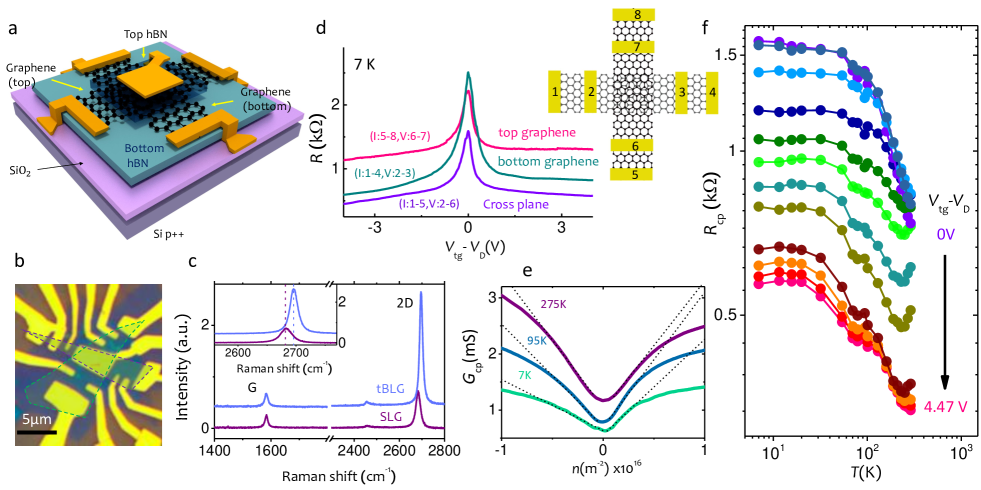
We assembled the tBLG devices with layer-by-layer mechanical transfer method, which is common in van der Waals epitaxy roy2013graphene ; karnatak2016current ; zomer2011transfer . Three devices were constructed which show very similar behavior, and we present the results from one of the devices here. The device consists of two graphene layers oriented in a “cross” configuration (inset of Fig. 1a and an optical micrograph in Fig. 1b), and entirely encapsulated within two layers of hexagonal boron nitride (hBN). The carrier mobilities in the upper and lower layers are cm2V-1s-1 and cm2V-1s-1, at room temperature, respectively. More detail on the fabrication process can be found in Methods. The doping density can be varied with the global back gate (heavily doped silicon substrate), as well as locally at the overlap region by using a lithographically defined top gate. Multiple contacts on all sides of the overlap region allow a four-probe measurement of both in-plane and cross-plane transport.

The difference in the Raman spectra from the overlap and the bare graphene regions in Fig. 1c, allows an estimation of the twist angle kim2012raman ; boschetto2013real ; havener2012angle ; he2013observation ; lui2015observation ; campos2013raman . For optical transitions in the parallel band model havener2012angle ; kim2012raman , the blue shift, intensity enhancement and width reduction of Raman peaks is attributed to van Hove singularities in the presence of weak interlayer interaction. The observed blue shift of cm-1 in the 2D peak position (inset of Fig. 1c) suggests , which is supported by the 2D peak width reduction and G band intensity as well (Fig. S1 of supplementary information).
Fig. 1d shows the effect of top gate voltage () on both in-plane and cross-plane electrical resistance, while the back gate voltage is held fixed at V to minimize the contribution of series resistance. The in-plane bipolar transfer characteristics are expected in graphene, while similar observation in the cross-plane transport can arise from two processes: (1) density-of-state-dependent incoherent tunneling across the van der Waals gap with interlayer conductance kim2013breakdown ; bistritzer2010transport , or (2) interlayer conduction limited by electron-phonon scattering perebeinos2012phonon with , where , , , and are the cross-plane electrical resistance, energy-dependent density-of-states of the th layer, interlayer transmission probability, Fermi energy of the graphene layers, and the thermal population of the out-of-plane beating phonon mode of energy , respectively. Although both mechanisms lead to , in agreement with the observations for small (Fig. 1e), they differ in their temperature dependences. As shown in Fig. 1f, the low cross-plane transport is -independent, which is consistent with incoherent quantum tunneling, whereas decreases sharply for K, suggesting the onset of phonon-driven electrical conduction as the thermal population of interlayer phonons increases with increasing . Since both mechanisms depend on in a similar manner, the crossover temperature scale ( K) varies weakly with doping, but serves as an indicator of the energy scale of interlayer phonons cocemasov2013phonons . The slight asymmetry at low temperature ( K) between the electron and the hole doped regimes is probably a series resistance effect outside the overlap region, because the two graphene layers exhibit different mobilities.
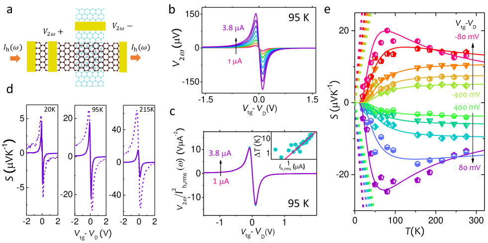
To measure the Seebeck effect across the van der Waals junction, we employ local Joule heating of one of the graphene layers, which establishes a interlayer temperature difference , while measuring the resulting thermal voltage generated between the layers (See schematic in Fig. 2a, and Methods). For a sinusoidal heating current of frequency , the thermal component is obtained from the second harmonic () of the cross-plane voltage zuev2009thermoelectric ; goswami2009highly . At fixed , varies with doping in a qualitatively similar manner as that observed for in-plane Seebeck effect in graphene zuev2009thermoelectric ; checkelsky2009thermopower (Fig. 2b), which is antisymmetric across the Dirac point, with the sign of representing that of the majority carriers. The thermal origin of can be readily verified from the scaling of over the entire range of (Fig. 2c). The interlayer temperature gradient is determined entirely by and (Inset of Fig. 2c) confirms that the thermoelectric power is independent of within the range of heating current (A) of our experiment (see Methods and supplementary information for details on the temperature calibration).

We first compared the dependence of on to that expected from the semiclassical Mott relation jonson1980mott ,
| (1) |
at three different values of . Evaluating the right hand side of Eq. 1 using the parallel plate capacitor model and linear dispersion of graphene, shows that the experimentally observed bears only a qualitative similarity to (shown as dotted lines in Fig. 2d), and decreases far more rapidly with increasing , than that expected from Eq. 1. A violation of the Mott relation goswami2009highly ; buhmann2013thermoelectric ; behnia2004thermoelectricity is possible in the presence of strong electron-electron interaction, or localized magnetic moments, but this cannot explain the enhanced suppression of from the Mott relation at higher doping (i.e. larger ), where the interaction effects are expected to be minimal. Fig. 2d also shows that the suppression of the observed from the Mott relation becomes stronger at higher , suggesting a likely role of interlayer phonons. To explore this further, the -dependence of at different is shown in Fig. 2e. The maximum of VK-1 occurs at mV, corresponding to cm-2, at K. The generic behavior of seems to indicate a characteristic temperature scale, which increases with , beyond which either weakly decreases (at low doping) or saturates to a finite value asymptotically (at high doping).
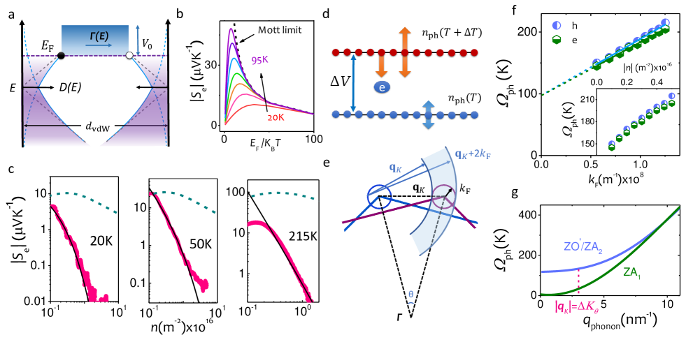
Modelling the tBLG as a tunnel junction with electronically decoupled graphene electrodes, the thermoelectric parameters can be directly computed with the Landauer-Buttiker formalism (See Fig. 3a and Methods for calculation details). At high doping, i.e. , the calculated (electron/hole symmetric) thermopower decreases along a universal trace as a function of (Fig. 3b). However, as , the inhomogeneity in the charge distribution, represented by a finite broadening of the dispersion relations in the layers, causes to vary in an inhomogeneity and temperature specific manner. A comparison in Fig. 3c reveals that the computed magnitude of from the Landauer-Buttiker formalism is orders of magnitude larger than the experimentally observed , especially at large , where the experimental decays much faster than that expected theoretically (dashed lines in Fig. 3c).

The observation of at low temperatures where the electrical conductance occurs through incoherent tunneling (Fig. 2e), suggests that thermoelectric transport in tBLG is likely driven by the electron-phonon coupling. A phenomenological description involves charge imbalance across the layers induced by the imbalance in the thermal population () of phonons so that , where is the interlayer potential difference (schematic in Fig. 3d). Hence,
| (2) |
where is the energy of the interlayer phonon mode that conserves momentum during the transfer of a charge from the Fermi surface of one graphene layer to that of the other ( and represent the vector in the reciprocal space connecting the Dirac points of the rotated Brillouine zones, and the Fermi wave vector, respectively). The prefactor embodies the electron-phonon coupling. Eq. 2 provides excellent fit to the observed -dependence of , shown by the solid lines in Fig. 2e, and allows us to estimate the which sets the characteristics scale in the dependence as a function of (inset of Fig. 3f). (In fitting the data for mV, a weak -dependence of , where was assumed.)
The observed magnitude of K, suggests that the low-energy ZO/ZA2 layer breathing phonon modes cocemasov2013phonons ; campos2013raman in tBLG, which determines the interlayer electrical conductance perebeinos2012phonon ; kim2013breakdown are also primarily responsible for thermoelectric transport across the van der Waals gap. However, to cross-verify this quantitatively, we assume the phenomenological phonon dispersion of the out-of-plane breathing modes perebeinos2012phonon , , where the momentum conservation requires phonons with average momentum to transfer charge between all points of the two Fermi surfaces ( schematic of Fig. 3e) (here, , and are the zone center phonon energy, bending stiffness and areal mass density of graphene, respectively). Since , one expects to have a linear dependence on , as indeed observed in Fig. 3f, and the slope of the linear dependence yields nm-1. This corresponds to a misorientation angle of , in excellent agreement with the estimate of from Raman measurements (Fig. 1c). The intercept, K, also agrees well with the ZO/ZA2 phonon branch energy ( K) for nm-1 perebeinos2012phonon ; cocemasov2013phonons ; campos2013raman , as shown by the vertical dashed line in Fig. 3g. Eq. 2 also captures the density dependence of shown in Fig. 3c if we choose a prefactor (solid lines Fig. 3c), although is found to be -dependent, varying from at low to at K.

The deviation of from the Mott relation (Eq. 1) is a key result of our experiments which demands further elaboration. The Mott relation is expected to hold even in the presence of phonon-driven tunneling, when the tunneling is isotropic (i.e. its amplitude depends only on the magnitude and not the direction of the momentum vector of the electron) and when the phonons are in thermal equilibrium. A non-equilibrium distribution of phonons can give rise to ‘cross-plane phonon drag’ (due to a transport of heat from one layer to another by the layer breathing modes in each) resulting in a violation of the Mott formula. Furthermore, and rather unusually, the measured thermopower is always smaller than the value obtained from the Mott formula (Fig. 2d). A drag component in the presence of umklapp scattering could, in principle reduce below the regular tunneling component given by Landauer-Buttiker formula and hence deviate from the Mott relation bailyn1967phonon . However, this is inconsistent with the observed dominance and the sign of the drag component in our devices. Hence, the violation of the Mott relation we observe is most likely due to a strong suppression of the regular tunneling component from the Mott value due to anisotropic tunneling arising from the twist between the layers.
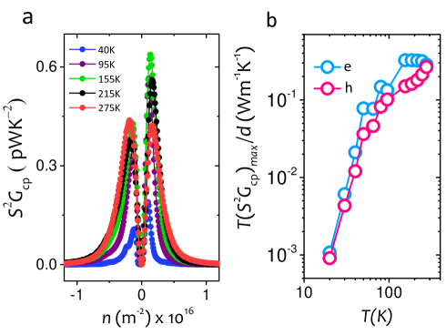
Finally, we have calculated the cross-plane thermoelectric power-factor (), by combining the experimentally observed magnitudes of and . Fig. 4a presents the nearly electron-hole symmetric power factor with a maximum value of pWK-2. The maximum in power-factor, observed at cm-2 in our case, is determined by the interplay of the increase of and decrease of with , and can further be improved in higher mobility devices, where the onset of inhomogeneous transport occurs at lower . The maximum effective PFT , where nm is the van der Waals distance, increases with temperature, and can be as high as Wm-1K-1 at room temperature (Fig. 4b). While this is about an order of magnitude smaller than in-plane PFT of high-mobility graphene duan2016high and transition metal dichalcogenides layers yoshida2016gate ; hippalgaonkar2015record , the phonon-filtering in cross-plane thermal transport may lead to lower thermal conductance, and hence a high figure-of-merit thermoelectric system pop2012thermal ; alofi2013thermal .
In conclusion, we have measured, for the first time, the thermoelectric properties across the van der Waals gap formed in twisted bilayer graphene. We demonstrated that the cross-plane thermoelectric transport is driven by the scattering of electrons and interlayer layer breathing phonon modes, which thus represents a unique “phonon drag” effect across atomic distances. Although the deviation from the Mott relations needs further understanding, we believe that clever engineering of van der Waals heterostructures, for example, inclusion of intermediate atomic layers from layered solids acting as phonon filters chen2015thermoelectric , may lead to exceptional cross-plane thermoelectric properties.
I Methods
I.1 Fabrication of hBN encapsulated tBLG devices
All devices in this work were fabricated using layer by layer mechanical transfer method where the overlap region of the two graphene layers, which forms the tBLG system, is encapsulated within two hBN layers to prevent surface contamination and minimize substrate and lithography effects. The top hBN layer also acts as the dielectric for the lithographically defined metal top gate. The electrical contacts to the individual layers were patterned using electron beam lithography (EBL). The electrical leads were mostly formed by etching through the hBN encapsulation, followed by a metallization step for edge-contacting the graphene layers. To achieve this, patterned contacts were exposed to reactive ion etching (RIE) to etch the top hBN. The metal deposition (5nm Cr/50nm Au) was then done by thermal evaporation technique to make electrical contact with the one dimensional edges of the single layer graphene channels.
I.2 Calculation of the temperature gradient across the van der Waals gap.
The temperature difference between the two monolayers is obtained by calibrating the individual in-plane resistances of the two monolayers as functions of both temperature and heating current at the charge neutrality point. The scaling of in Fig. 2c over the entire range of confirms that the is solely proportional to the heating current and independent of the doping induced by the top gate. The independent scaling of with and with (inset Fig. 2c) confirms that the all the measurements were done in the linear heating response regime and the condition is maintained throughout.
I.3 Theoretical calculation.
We have employed a phenomenological metal-insulator-metal junction model, where the interlayer tunneling occurs with tunneling probability . The Seebeck coefficient can then be written as,
where the density-of-states are for pristine graphene layers, and is the Fermi function. In order to incorporate the effect of inhomogeneity at very low energies, we have parametrized the potential fluctuations with a broadening constant as shown in the schematic of Fig. 3a, where meV is estimated from the experimental transport parameters.
II acknowledgement
The authors thank the financial support from the Department of Science and Technology, Government of India. P.S.M. and A.G. thank the National Nanofabrication Center, CeNSE, IISc (NNfC) for clean room fabrication facilities and the Micro and Nano Characterization Facility, CeNSE, IISc (MNCF) for optical and mechanical characterization facilities.
References
- (1) Koren, E. et al. Coherent commensurate electronic states at the interface between misoriented graphene layers. Nat. Nanotech. 11, 752–757 (2016).
- (2) Perebeinos, V., Tersoff, J. & Avouris, P. Phonon-mediated interlayer conductance in twisted graphene bilayers. Phys. Rev. Lett. 109, 236604 (2012).
- (3) Kim, Y. et al. Breakdown of the interlayer coherence in twisted bilayer graphene. Phys. Rev. Lett. 110, 096602 (2013).
- (4) Dos Santos, J. L., Peres, N. & Neto, A. C. Graphene bilayer with a twist: Electronic structure. Phys. Rev. Lett. 99, 256802 (2007).
- (5) Boschetto, D. et al. Real-time observation of interlayer vibrations in bilayer and few-layer graphene. Nano Lett. 13, 4620–4623 (2013).
- (6) Cocemasov, A. I., Nika, D. L. & Balandin, A. A. Phonons in twisted bilayer graphene. Phys. Rev. B 88, 035428 (2013).
- (7) Lui, C. H. et al. Observation of interlayer phonon modes in van der Waals heterostructures. Phys. Rev. B 91, 165403 (2015).
- (8) Luican, A. et al. Single-layer behavior and its breakdown in twisted graphene layers. Phys. Rev. Lett. 106, 126802 (2011).
- (9) Ohta, T. et al. Evidence for interlayer coupling and moire periodic potentials in twisted bilayer graphene. Phys. Rev. Lett. 109, 186807 (2012).
- (10) Ding, Z., Pei, Q.-X., Jiang, J.-W., Huang, W. & Zhang, Y.-W. Interfacial thermal conductance in graphene/MoS2 heterostructures. Carbon 96, 888–896 (2016).
- (11) Zhang, Z., Xie, Y., Peng, Q. & Chen, Y. Thermal transport in MoS2/graphene hybrid nanosheets. Nanotechnology 26, 375402 (2015).
- (12) Sadeghi, H., Sangtarash, S. & Lambert, C. J. Cross-plane enhanced thermoelectricity and phonon suppression in graphene/MoS2 van der Waals heterostructures. 2D Mater. 4, 015012 (2016).
- (13) Chen, C.-C., Li, Z., Shi, L. & Cronin, S. B. Thermoelectric transport across graphene/hexagonal boron nitride/graphene heterostructures. Nano Res. 8, 666–672 (2015).
- (14) Hung Nguyen, V., Nguyen, M. C., Nguyen, H.-V., Saint-Martin, J. & Dollfus, P. Enhanced thermoelectric figure of merit in vertical graphene junctions. Appl. Phys. Lett. 105, 133105 (2014).
- (15) Juang, Z.-Y. et al. Graphene-Au nanoparticle based vertical heterostructures: A novel route towards high-ZT thermoelectric devices. Nano Energy 38, 385–391 (2017).
- (16) Roy, K. et al. Graphene-MoS2 hybrid structures for multifunctional photoresponsive memory devices. Nat. Nanotech. 8, 826–830 (2013).
- (17) Karnatak, P. et al. Current crowding mediated large contact noise in graphene field-effect transistors. Nat. Commun. 7 (2016).
- (18) Zomer, P., Dash, S., Tombros, N. & Van Wees, B. A transfer technique for high mobility graphene devices on commercially available hexagonal boron nitride. Appl. Phys. Lett. 99, 232104 (2011).
- (19) Kim, K. et al. Raman spectroscopy study of rotated double-layer graphene: misorientation-angle dependence of electronic structure. Phys. Rev. Lett. 108, 246103 (2012).
- (20) Havener, R. W., Zhuang, H., Brown, L., Hennig, R. G. & Park, J. Angle-resolved Raman imaging of interlayer rotations and interactions in twisted bilayer graphene. Nano Lett. 12, 3162–3167 (2012).
- (21) He, R. et al. Observation of low energy Raman modes in twisted bilayer graphene. Nano Lett. 13, 3594–3601 (2013).
- (22) Campos-Delgado, J., Cançado, L. G., Achete, C. A., Jorio, A. & Raskin, J.-P. Raman scattering study of the phonon dispersion in twisted bilayer graphene. Nano Res. 6, 269–274 (2013).
- (23) Bistritzer, R. & MacDonald, A. H. Transport between twisted graphene layers. Phys. Rev. B 81, 245412 (2010).
- (24) Zuev, Y. M., Chang, W. & Kim, P. Thermoelectric and magnetothermoelectric transport measurements of graphene. Phys. Rev. Lett. 102, 096807 (2009).
- (25) Goswami, S. et al. Highly enhanced thermopower in two-dimensional electron systems at millikelvin temperatures. Phys. Rev. Lett. 103, 026602 (2009).
- (26) Checkelsky, J. G. & Ong, N. Thermopower and Nernst effect in graphene in a magnetic field. Phys. Rev. B 80, 081413 (2009).
- (27) Jonson, M. & Mahan, G. Mott’s formula for the thermopower and the Wiedemann-Franz law. Phys. Rev. B 21, 4223 (1980).
- (28) Buhmann, J. M. & Sigrist, M. Thermoelectric effect of correlated metals: Band-structure effects and the breakdown of Mott’s formula. Phys. Rev. B 88, 115128 (2013).
- (29) Behnia, K., Jaccard, D. & Flouquet, J. On the thermoelectricity of correlated electrons in the zero-temperature limit. J. Phys. Cond. Matter 16, 5187 (2004).
- (30) Bailyn, M. Phonon-drag part of the thermoelectric power in metals. Phys. Rev. 157, 480 (1967).
- (31) Duan, J. et al. High thermoelectricpower factor in graphene/hBN devices. Proc. Natl Acad. Sci. 113, 14272–14276 (2016).
- (32) Yoshida, M. et al. Gate-optimized thermoelectric power factor in ultrathin WSe2 single crystals. Nano Lett. 16, 2061–2065 (2016).
- (33) Hippalgaonkar, K. et al. Record high thermoelectric powerfactor in single and few-layer MoS2. arXiv preprint arXiv:1505.06779 (2015).
- (34) Pop, E., Varshney, V. & Roy, A. K. Thermal properties of graphene: Fundamentals and applications. MRS bulletin 37, 1273–1281 (2012).
- (35) Alofi, A. & Srivastava, G. Thermal conductivity of graphene and graphite. Phys. Rev. B 87, 115421 (2013).