Antiferromagnetic domain wall motion driven by polarized spin waves
Abstract
The control of magnetic domain walls is essential for the magnetic-based memory and logic applications. As an elementary excitation of magnetic order, spin wave is capable of moving magnetic domain walls just as the conducting electric current. Ferromagnetic spin waves can only be right-circularly polarized. In contrast, antiferromagnetic spin waves have full polarization degree of freedom, including both left- and right-circular polarizations, as well as all possible linear or elliptical ones. Here we demonstrate that, due to the Dzyaloshinskii-Moriya interaction, the spin wave driven domain wall motion in antiferromagnets strongly depends on the linear polarization direction of the injected spin waves. Steering domain wall motion by simply tuning the polarization of spin waves offers new designing principles for domain-wall based information processing devices.
Introduction. Magnetic domain walls widely exist in all ferro-, ferri-, and antiferro-magnetic materials. Controlling domain wall motion in a precise and convenient way is of great interest for both fundamental physics and industrial applications Allwood et al. (2002, 2005); Parkin et al. (2008). The domain wall motion has been studied extensively, and is found to be driven by external magnetic field Schryer and Walker (1974); Nakatani et al. (2003), spin transfer torque Berger (1978); Yamaguchi et al. (2004); Tatara and Kohno (2004); Thiaville et al. (2005), spin orbital torque Miron et al. (2011); Emori et al. (2013); Ryu et al. (2013), as well as spin waves Yan et al. (2011); Tveten et al. (2014); Kim et al. (2014); Wang et al. (2015); Qaiumzadeh et al. (2017). It has been shown that the antiferromagnetic domain wall can be driven more efficiently and moves much faster than its ferromagnetic counterpart Yang et al. (2015); Gomonay et al. (2016); Shiino et al. (2016), which makes antiferromagnet more appealing for future magnetic-based information storage and processing techniques.
The current-driven domain wall motion via the spin transfer torque Berger (1978); Yamaguchi et al. (2004); Tatara and Kohno (2004); Thiaville et al. (2005) or spin orbital torque Miron et al. (2011); Emori et al. (2013); Ryu et al. (2013) relies on the conduction electrons, which are not favorable for energy efficiency. In contrast, the spin wave driven domain wall motion Yan et al. (2011); Tveten et al. (2014); Kim et al. (2014); Wang et al. (2015); Qaiumzadeh et al. (2017) does not involve any physical motion of conduction electrons, therefore avoids the Joule heating completely. In addition, the spin wave, as an magnetic excitation upon the static magnetization texture, is intrinsically compatible with the background magnetic texture itself Lan et al. (2015). Therefore, by using static magnetic structures for memory and dynamical excitations for processing, it is possible to achieve information memory and processing simultaneously on a common magnetic system Yu et al. (tion).
With two opposite magnetic sublattices, antiferromagnetic spin waves are endowed with full polarization degrees of freedom Tveten et al. (2014); Cheng et al. (2014, 2016); Lan et al. (2017). Similar to photonics Goldstein (2003), it is more natural and convenient to encode information in the polarization degree of freedom than other degrees of freedom such as amplitude or phase. Above all, the interplay between the polarized spin wave and magnetic texture in antiferromagnet would be extremely beneficial for magnonic applications.
Previously, the present authors have shown that a simple antiferromagnetic domain wall surprisingly works as a spin wave polarizer and waveplate Lan et al. (2017), thus is capable in manipulating spin wave polarization in full flexibility. In this Letter, we study the equally important inverse effect, i.e. the back reaction of spin wave on the domain wall, and we find that the spin wave driven antiferromagnetic domain wall motion strongly depends on the linear polarization of the injected spin waves. This polarization-dependent domain wall motion effect, in combination with its inverse process of polarizing spin waves by domain wall Lan et al. (2017), provides a simple scheme in exchanging binary information between the dynamical spin waves and static magnetic textures. Our findings could lead to future logic-in-memory (or processing-in-memory) computing units solely based on magnetic systems Yu et al. (tion).

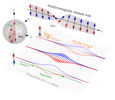
Model. Let us consider a domain wall structure in an antiferromagnetic wire along direction as shown in Fig. 1, where the red (blue) arrows denote the magnetization directions in the two magnetic sublattices. We define the normalized staggered Néel order and the total magnetization . With the constraint , the dyanmics of the staggered field is governed by Tveten et al. (2013, 2014); Kim et al. (2014); Tveten et al. (2016)
| (1) |
and becomes a slave quantity. Here is the effective field acting on , where and are the angular momentum line density and the saturation magnetization of one sublattice with the cross section area . And is the damping constants for the staggered field . The free energy , where and are the inter/intra-sublattice exchange constants, is the easy-axis anisotropy (along -axis), and is the strength of the Dzyaloshinskii-Moriya interaction (DMI).
We denote the static profile of the antiferromagnetic domain wall along -axis by the staggered field , where and are the polar and azimuthal angle of with respect to . Regardless of the presence of the DMI, an antiferromagnetic domain wall in Fig. 1 always takes the Walker type profile like its ferromagnetic counterpart with and Yan et al. (2011); Lan et al. (2015, 2017); Tveten et al. (2014), where is the characteristic domain wall width and is the position of the center of the domain wall. The magnetization directions in a domain wall along trace out a plane in the Bloch sphere in spin space (see Fig. 1). This plane forms an angle relative to - plane. When DMI is present, because the (bulk-type) DMI prefers neighbouring magnetizations to rotate about the -axis or in the - plane, the Bloch type domain wall (, as pictured in Fig. 1) has lower energy than the Néel type (). Therefore, DMI breaks the spin rotation symmetry of the domain wall in with respect to .
Spin wave in an antiferromagnetic domain wall. With the static domain wall profile , let and be the dynamical spin wave excitations upon the static , where and are the local transverse (polar and azimuthal) directions with respect to the static as depicted in Fig. 1. By linearizing Eq. (1), the equations of motion for the transverse component of the staggered field reduce to two decoupled Klein-Gordon equations Tveten et al. (2014),
| (2a) | ||||
| (2b) | ||||
where the effects of the inhomogeneous texture of the domain wall are transformed into two effective potentials and : is a potential well due to the easy-axis anisotropy along , and is a potential barrier due to the combined action of DMI and the inhomogeneous magnetic texture Lan et al. (2017). Eq. (2) describes the behavior of the spin wave modes polarizing along the - and -direction, respectively. Since the transverse direction () is in (perpendicular to) the magnetization rotation plane as seen in Fig. 1, we call modes the in-plane and out-of-plane modes, which also coincide with the - and -polarized modes in the region far away from the domain wall. Away from the domain wall, and , the - and -polarized spin wave modes are degenerated with the standard antiferromagnetic dispersion Kittel (1951); Keffer and Kittel (1952). This dispersion indicates that antiferromagnetic spin wave can be regarded as massive relativistic particles of rest mass determined by the spin wave gap and the effective “speed of light” Haldane (1983); Kim et al. (2014); Shiino et al. (2016).

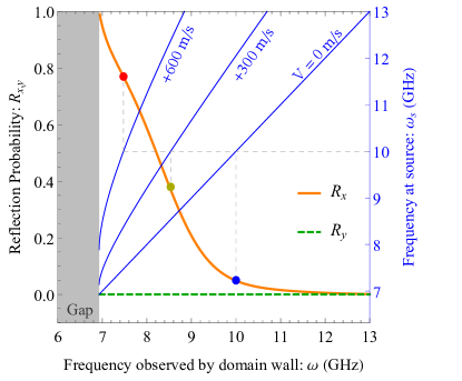
Both effective potentials and are localized at the domain wall. in Eq. (2a) is the reflectionless Pöschl-Teller type potential Poschl and Teller (1933). Therefore, the (in-plane) -polarized spin wave modes pass through the domain wall perfectly. On the other hand, the (out-of-plane) -polarized spin wave modes are expected to experience reflections because of the additional barrier potential caused by DMI in Eq. (2b). Consequently, this polarization dependent scattering at an antiferromagnetic domain wall gives rise to the polarizing effect as demonstrated in Ref. [Lan et al., 2017]. The frequency dependence of the reflection probability calculated from Eq. (2) is shown in Fig. 2, where identically for all frequencies and decreases from unity to zero as frequency increases. In practice, the reflection probability also depends on the domain wall velocity relative to the spin wave source due to the (relativistic) Doppler effect. Therefore, as the domain wall moves, the realized reflection probability relies on the observed frequency at the domain wall rather than the frequency at the spin wave source as shown in Fig. 2.

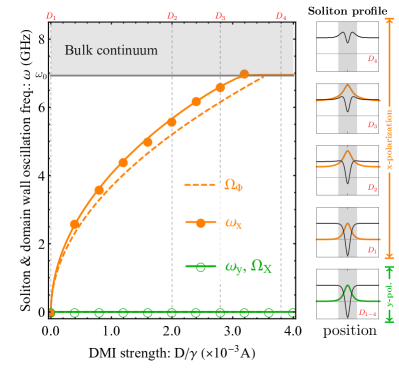
Apart from the scattering spin waves, Eq. (2) also hosts an in-plane and an out-of-plane soliton spin wave modes. When DMI vanishes: , both soliton modes are gapless and have zero frequency with profile . When DMI is present: , the in-plane soliton mode remain gapless at ; but the out-of-plane soliton mode in Eq. (2b) becomes gapped and has a finite frequency: . As DMI strength increases, the frequency approaches the bulk spin wave gap , and finally merges into the bulk continuum as shown in Fig. 3. Such behavior can also be understood as that the out-of-plane (x-polarized) soliton mode is expelled as the potential well becomes shallower and shallower with increasing , as seen in the right column of Fig. 3.
In fact, the two soliton modes are directly linked to the domain wall motion and rotation. In rigid domain wall model Schryer and Walker (1974); Tatara and Kohno (2004); Thiaville et al. (2005); Tveten et al. (2014); Kim et al. (2014); Wang et al. (2015); Shiino et al. (2016); Yang et al. (2015); Gomonay et al. (2016); Qaiumzadeh et al. (2017), the dynamics of a domain wall can be described by the time evolution of its position and rotation angle , which represents the translation of the domain wall along and the spin rotation of the domain wall about respectively. In the absence of the external driving forces, by integrating over the whole space Tveten et al. (2014); Kim et al. (2014), Eq. (1) becomes the Newtonian-like equations for and :
| (3a) | ||||
| (3b) | ||||
where and are effective mass and moment of inertia of the antiferromagnetic domain wall, respectively. And are the viscosity for translational and rotational motion. is the effective pinning torque induced by DMI, whose effect is to restore the domain wall to the Bloch type (). The decoupled dynamics for the position and rotation angle means that domain wall translation and rotation are two independent degrees of freedom in antiferromagnet.
Eq. (3) gives rise to two domain wall oscillating modes: one for the oscillation of the domain wall position in real space, and the other for the oscillation of the domain wall rotation angle in spin space. When DMI is absent: , they are two Goldstone modes with vanishing frequency: and constant displacement in real and spin space: and When DMI is present: the oscillating frequency for is unaffected: . But the oscillating frequency for becomes finite: due to the pinning torque , which breaks the the rotational symmetry about in spin space, and always tries to restore the rotation plane back to the - plane.
The frequencies of the two oscillating modes of the antiferromagnetic domain wall coincide with that of the two soliton modes above: and . This is no accidental: the soliton picture and the rigid domain wall picture are merely two different viewpoints about the same domain wall distortion. Fig. 3 shows that the frequencies of the soliton modes calculated from Eq. (2) and that of the oscillating modes calculated from Eq. (3) indeed agree with each other, and also in agreement with the micromagnetic simulation based on the full coupled LLG equation in terms of (see Method).
Spin wave driven domain wall motion. With Eq. (3), we are ready to include the effect of driving forces. As of interests of this Letter, we consider spin wave injection, thus we need to take into account the linear momentum and the angular momentum of the spin wave transferred to the domain wall. The linear momentum is transferred via the spin wave reflection, and the resulting force pushes the domain wall forward. The angular momentum transfered gives rise to a torque driving the domain wall in rotation. In this study, we assume that the domain wall dynamics in chirality angle is frozen because of the pinning torque , and we only focus the dynamics in domain wall position . Eq. (3a) is modified with the spin wave force Kim et al. (2014); Tveten et al. (2014); Qaiumzadeh et al. (2017)
| (4) |
The force exerted by the spin wave on domain wall is determined by the momentum of the reflected spin waves, which depends on the linear polarization and the frequency of the injected spin wave, as well as the domain wall velocity as shown in Fig. 2. Assuming that the injected spin wave is linearly polarized along or and has frequency and wavevector , assuming that the domain wall is at rest , then Kim et al. (2014); Tveten et al. (2014); Qaiumzadeh et al. (2017)
| (5) |
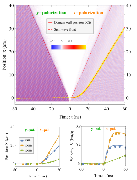
where is the amplitude of the injected spin wave with polarization , and is the reflection probability for polarization . Because the reflection probabilities for - and -polarized spin waves are drastically different: and , we expect that the domain wall motion should strongly depend on the spin wave polarization. Fig. 4(a) shows exactly that the -polarized spin wave reflects at the domain wall and drives the domain wall forward, while the -polarized spin wave pass through and the domain wall basically stays at rest (also see Supplementary Movies). .
The force in Eq. (5) is valid only when the domain wall does not move relative to the spin wave source, i.e. . In order to calculate the domain wall position and velocity as function of time quantitatively, we have to take into account the relativistic Doppler effect of a moving domain wall driven by the spin wave. Therefore the frequency/wavevector used in Eq. (5) should be replaced by their values observed by the moving domain wall: Kim et al. (2014):
| (6) |
with . In the mean time, the moving domain wall also becomes narrower and more massive in the lab reference frame due to the relativistic effect: Kim et al. (2014). When including all relativistic effect of a moving domain wall in Eq. (4), we can compute the time dependence of the domain wall position and velocity . This frequency/wavevector change is important because the reflection probability , thus the force , strongly depends on the frequency seen by the domain wall (see Fig. 2). Therefore, the reflection probability varies in a non-trivial way as the domain wall accelerates, and the resulting domain wall velocity is a non-linear function of time.
Fig. 4(a) plots as function of position and time obtained by micromagnetic simulations, where the cases with -polarized (at right side) and -polarized (at left side) spin wave injection are put side by side. The spin wave source is located at m. Much information is contained in this plot: i) the domain wall center (with ) is indicated by the yellowish spot in the color plot, and the spin wave excitation is in red and blue, ii) the domain wall is transparent for -polarization and opaque for -polarization as expected, iii) because of ii) the domain wall moves forward with -polarized spin wave, and stays at rest with -polarized spin wave, iv) the wave-front travels with the spin wave group velocity as expected. The solid curve plots the domain wall position calculated from Eq. (4), and the dashed line is plotted using the group velocity of the injected spin wave. Both curves agree perfectly with the micromagnetic simulations. Fig. 4(b) shows the comparison between results from the micromagnetic simulation and the results calculated using Eq. (4) for several driving frequencies. They all agree with each other very well for both positions and velocities.

Discussions. The reflection of linearly polarized spin wave at the antiferromagnetic domain wall discussed in this Letter is different from the reflection of circularly polarized spin wave discussed by Tveten et al. Tveten et al. (2014); Kim et al. (2014); Qaiumzadeh et al. (2017) The essential difference is that, in the later case, the injected circularly polarized spin wave first drives the domain wall in precession, then the precession causes the reflection. However, in our case, the presence of DMI hinders the domain wall precession, and the -polarized spin wave is reflected by the domain wall simply because DMI does not favor the -polarization in the wall.
We demonstrated here the polarization dependent spin wave driven domain wall motion in antiferromagnetic wires with the bulk-type DMI. The working principle is the same for the interfacial-type DMI, for which the roles of the - and -polarization interchange. Furthermore, everything discussed here work in both the real antiferromagnet and the synthetic antiferromagnet consisting of two coupled ferromagnets Yang et al. (2015). For real antiferromagnet, due to the promoted exchange coupling, the spin wave group velocity and domain wall velocity can be further boosted Shiino et al. (2016); Gomonay et al. (2016).
Conclusion. In conclusion, we demonstrated that, due to the spin rotation symmetry broken caused by the DMI, the spin wave driven domain wall motion in antiferromagnet depends on the linear polarization direction of incident spin waves, i.e. the antiferromagnetic domain wall moves with one linear polarization and stays at rest with the other orthogonal polarization. This direct connection between the polarization of the driving spin wave and the magnetic texture paves new routes in designing domain wall based magnetic logic and memory devices.
Method. A synthetic antiferromagnetic wire is used in micromagnetic simulations. The magnetic dynamics is described by two coupled Landau-Lifshitz-Gilbert (LLG) equations:
where denote the two sublattices, is the gyromagnetic ratio, is the Gilbert damping constant. Here (with and ) is the effective magnetic field acting locally on sublattice , where is the easy-axis anisotropy along , and are the Heisenberg and Dzyaloshinskii-Moriya exchange coupling constant within each sublattice, and is the exchange coupling constant between two sublattices. The parameters used are as below Yan et al. (2011); Lan et al. (2015, 2017): the easy-axis anisotropy , the exchange constant , the DMI constant , the inter-layer coupling is chosen to , the saturation magnetization , the gyromagnetic ratio , the damping , and vacuum permeability . The dipolar interaction is neglected for this antiferromagnetic environment. The micromagnetic simulations are performed in COMSOL Multiphysics, where the LLG equation is transformed into weak form by using the mathematical module and solved by the generalized-alpha method COM .
References
- Allwood et al. (2002) D. A. Allwood, G. Xiong, M. D. Cooke, C. C. Faulkner, D. Atkinson, N. Vernier, and R. P. Cowburn, Science 296, 2003 (2002).
- Allwood et al. (2005) D. A. Allwood, G. Xiong, C. C. Faulkner, D. Atkinson, D. Petit, and R. P. Cowburn, Science 309, 1688 (2005).
- Parkin et al. (2008) S. S. P. Parkin, M. Hayashi, and L. Thomas, Science 320, 190 (2008).
- Schryer and Walker (1974) N. L. Schryer and L. R. Walker, J. Appl. Phys. 45, 5406 (1974).
- Nakatani et al. (2003) Y. Nakatani, A. Thiaville, and J. Miltat, Nat. Mater. 2, 521 (2003).
- Berger (1978) L. Berger, J. Appl. Phys. 49, 2156 (1978).
- Yamaguchi et al. (2004) A. Yamaguchi, T. Ono, S. Nasu, K. Miyake, K. Mibu, and T. Shinjo, Phys. Rev. Lett. 92, 077205 (2004).
- Tatara and Kohno (2004) G. Tatara and H. Kohno, Phys. Rev. Lett. 92, 086601 (2004).
- Thiaville et al. (2005) A. Thiaville, Y. Nakatani, J. Miltat, and Y. Suzuki, Euro. Phys. Lett. 69, 990 (2005).
- Miron et al. (2011) I. M. Miron, T. Moore, H. Szambolics, L. D. Buda-Prejbeanu, S. Auffret, B. Rodmacq, S. Pizzini, J. Vogel, M. Bonfim, A. Schuhl, and G. Gaudin, Nat. Mater. 10, 419 (2011).
- Emori et al. (2013) S. Emori, U. Bauer, S.-M. Ahn, E. Martinez, and G. S. D. Beach, Nat. Mater. 12, 611 (2013).
- Ryu et al. (2013) K.-S. Ryu, L. Thomas, S.-H. Yang, and S. Parkin, Nat. Nano. 8, 527 (2013).
- Yan et al. (2011) P. Yan, X. S. Wang, and X. R. Wang, Phys. Rev. Lett. 107, 177207 (2011).
- Tveten et al. (2014) E. G. Tveten, A. Qaiumzadeh, and A. Brataas, Phys. Rev. Lett. 112, 147204 (2014).
- Kim et al. (2014) S. K. Kim, Y. Tserkovnyak, and O. Tchernyshyov, Phys. Rev. B 90, 104406 (2014).
- Wang et al. (2015) W. Wang, M. Albert, M. Beg, M.-A. Bisotti, D. Chernyshenko, D. Cortes-Ortuno, I. Hawke, and H. Fangohr, Phys. Rev. Lett. 114, 087203 (2015).
- Qaiumzadeh et al. (2017) A. Qaiumzadeh, L. A. Kristiansen, and A. Brataas, arXiv:1705.01572 [cond-mat] (2017).
- Yang et al. (2015) S.-H. Yang, K.-S. Ryu, and S. Parkin, Nat. Nano. 10, 221 (2015).
- Gomonay et al. (2016) O. Gomonay, T. Jungwirth, and J. Sinova, Phys. Rev. Lett. 117, 017202 (2016).
- Shiino et al. (2016) T. Shiino, S.-H. Oh, P. M. Haney, S.-W. Lee, G. Go, B.-G. Park, and K.-J. Lee, Phys. Rev. Lett. 117, 087203 (2016).
- Lan et al. (2015) J. Lan, W. Yu, R. Wu, and J. Xiao, Phys. Rev. X 5, 041049 (2015).
- Yu et al. (tion) W. Yu, J. Lan, and J. Xiao, (in preparation).
- Cheng et al. (2014) R. Cheng, J. Xiao, Q. Niu, and A. Brataas, Phys. Rev. Lett. 113, 057601 (2014).
- Cheng et al. (2016) R. Cheng, M. W. Daniels, J.-G. Zhu, and D. Xiao, Sci. Rep. 6, 24223 (2016).
- Lan et al. (2017) J. Lan, W. Yu, and J. Xiao, Nat. Commun. 8, 178 (2017).
- Goldstein (2003) D. Goldstein, Polarized Light Second Edition, Revised and Expanded (Marcel Dekker, New York, 2003).
- Tveten et al. (2013) E. G. Tveten, A. Qaiumzadeh, O. A. Tretiakov, and A. Brataas, Phys. Rev. Lett. 110, 127208 (2013).
- Tveten et al. (2016) E. G. Tveten, T. Müller, J. Linder, and A. Brataas, Phys. Rev. B 93, 104408 (2016).
- Kittel (1951) C. Kittel, Phys. Rev. 82, 565 (1951).
- Keffer and Kittel (1952) F. Keffer and C. Kittel, Phys. Rev. 85, 329 (1952).
- Haldane (1983) F. D. M. Haldane, Phys. Rev. Lett. 50, 1153 (1983).
- Poschl and Teller (1933) G. Poschl and E. Teller, Z. Phys. 83, 143 (1933).
- (33) “COMSOL Multiphysics,” http://comsol.com/.