Evolution of Nanowire Transmons and Their Quantum Coherence in Magnetic Field
Abstract
We present an experimental study of nanowire transmons at zero and applied in-plane magnetic field. With Josephson non-linearities provided by the nanowires, our qubits operate at higher magnetic fields than standard transmons. Nanowire transmons exhibit coherence up to , where the induced superconducting gap in the nanowire closes. We demonstrate that on-chip charge noise coupling to the Josephson energy plays a dominant role in the qubit dephasing. This takes the form of strongly-coupled two-level systems switching on timescales and a more weakly coupled background producing noise. Several observations, including the field dependence of qubit energy relaxation and dephasing, are not fully understood, inviting further experimental investigation and theory. Using nanowires with a thinner superconducting shell will enable operation of these circuits up to , a regime relevant for topological quantum computation.
Circuit quantum electrodynamics (cQED) offers unprecedented control over coupled atomic and photonic degrees of freedom in engineerable, microscale superconducting circuits Blais et al. (2004); Wallraff et al. (2004). It relies crucially on the dissipationless nonlinearity of the Josephson effect between two weakly coupled superconductors Josephson (1962). The Josephson junction (JJ), usually implemented in the form of superconductor–insulator–superconductor (SIS) junctions, allows the realization of anharmonic oscillators that can be operated in the quantum regime and used as qubits Nakamura et al. (1999). Circuit QED has found applications in many areas, including scaleable quantum computation Barends et al. (2014), quantum optics Steffen et al. (2013), quantum foundations Jerger et al. (2016) and quantum measurement and control Ristè et al. (2013). So far, cQED has been limited by standard SIS JJs based on aluminum and its oxide to fields , the critical field of bulk aluminum Harris and Mapother (1968). However, interesting applications such as coupling cQED devices to polarized electron-spin ensembles serving as quantum memories Imamoglu (2009) and using qubits as charge-parity detectors in Majorana based topological quantum computation Hyart et al. (2013); Mourik et al. (2012) require fields of . In such fields, more fundamental effects such as topological phase transitions Kosterlitz and Thouless (1973) and degeneracy-lifting of the Andreev bound states which underlie the Josephson effect Andreev (1964); Pillet et al. (2010); van Woerkom et al. (2017); Yokoyama et al. (2013) can be studied. Entering this important regime for cQED requires the use of field-compatible superconductors and non-standard JJs Samkharadze et al. (2016); Popinciuc et al. (2012); Doh et al. (2005); Pallecchi et al. (2008); Della Rocca et al. (2007).
To date, qubits in cQED architectures have been realized using various JJs: the ubiquitous SIS tunnel junction Nakamura et al. (1999), atomic break junctions Janvier et al. (2015) and semiconductor weak-link nanowire junctions de Lange et al. (2015); Larsen et al. (2015); Casparis et al. (2016). Nanowire qubits are of particular interest because of potential high-magnetic field compatibility, the voltage tunability of the JJ and the overlap with other technologies of interest, including nanowire-based transistors and lasers Chuang et al. (2013); Liu et al. (2015). Nanowire qubits are compatible with the transmon geometry Koch et al. (2007), the most widely used in cQED, and have been realized in flux and voltage tunable variants Larsen et al. (2015); de Lange et al. (2015). Nanowire transmons have reached echo dephasing times () up to 10 , and been used to implement two-qubit gates Casparis et al. (2016). So far, the use of Al as a superconductor for the larger scale cQED elements Larsen et al. (2015); Casparis et al. (2016) and short coherence times de Lange et al. (2015) have inhibited study of the coherence of these circuits in a magnetic field.
In this Letter, we characterize noise processes affecting nanowire transmons and explore their behavior in an in-plane magnetic field (). Using a flux-tunable split-junction device, we first achieve limited by energy relaxation () at the flux sweet spot. Independent of the flux-noise reducing coherence away from the sweet spot, the qubit coherence suffers from a charge two-level system (TLS) strongly coupled to the nanowire Josephson energy , leading to a switching of the qubit frequency (). The TLS switching is observed in real time using a single-shot, frequency-detecting pulse sequence giving characteristic switching times of 100 Ristè et al. (2013). We also observe this frequency switching in side-gate-tunable single-junction qubits (gatemons) and show that it is sensitive to the applied side-gate voltage . In addition to these strongly coupled TLSs, a weakly coupled charge-noise background is also investigated. Finally, we study the behavior of a gatemon in applied , observing reduced as the superconducting gap () induced in the nanowire is suppressed. While both and are reduced due to , an effect not yet understood, the device exhibits measurable coherence up to .
The device fabrication combines procedures widely used in cQED with nanowire etching and contacting recipes. Large features on the chips (ground plane, waveguides and transmon capacitors) are defined by a reactive-ion etch of the NbTiN film on the high-resistivity silicon substrate Thoen et al. (2017); Bos et al. (2017); Bruno et al. (2015). The nanowires used to create the superconductor-semiconductor-superconductor (SNS) junction have an InAs core and an epitaxially grown Al shell that induces a hard superconducting gap, suppressing quasiparticle tunneling Doh et al. (2005); Chang et al. (2015); Martinis et al. (2009); Wang et al. (2014). They are deterministically placed in the contacting region using a nanomanipulator. The individual positions of the nanowires are analyzed using a home-developed image recognition software that automatically defines etch- and contacting masks SM ; Itseez (2015). After defining the SNS junction by wet-etching a 200 segment of the 30 thick Al shell, the wires are contacted with NbTiN. The qubits are individually coupled to dedicated readout resonators which each couple to a common feedline, allowing for multiplexed readout Jerger et al. (2012). Standard cQED control and measurements schemes are used to probe the qubits Blais et al. (2004); Motzoi et al. (2009).
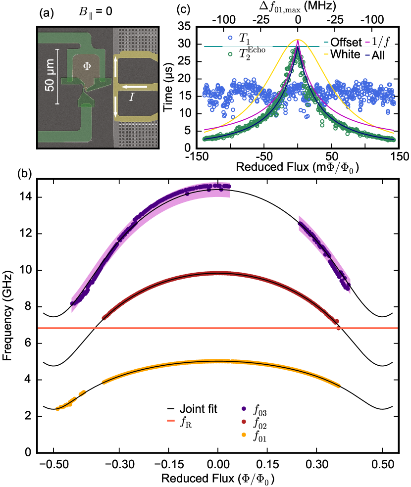
We start by studying the spectrum of the flux-tunable, split-junction device, to extract information about the SNS junctions. Applying a current through the flux-bias line changes the magnetic flux through the SQUID loop [Fig. 1(a)] and thus controls the superconducting phase difference between the two transmon islands. This phase difference tunes in each junction, given in the short-junction, single-channel limit by Andreev bound states with transmission probability and energy . Employing the Andreev bound state model in the split-junction Cooper-pair box type Hamiltonian, , yields good agreement with the observed spectrum [Fig. 1(b)], as in de Lange et al. (2015). The best-fit values of the induced gaps and are close to the bulk Al gap of 43 . This shows that the Al shell fully proximitizes the nanowire Wang et al. (2014).
We investigate the flux noise of the split-junction qubit by measuring coherence times as a function of flux offset. The is limited at the flux sweet spot, but is reduced as the sensitivity to flux noise increases [Fig. 1(c)]. The noise is quantified using a quadratic fit to the echo dephasing rate plotted against Martinis et al. (2003); Yoshihara et al. (2006); Hutchings et al. (2017); SM . A least-squares fit yields a white-noise contribution , a noise amplitude where and a flux-independent offset of 2 . The small size of the flux-independent offset demonstrates that the transport through the nanowire junction is highly coherent. The value of the flux noise amplitude is a factor of larger than that of SIS transmons Hutchings et al. (2017). The origin of the observed white noise contribution that is typically absent in flux-tunable transmon qubits is unclear.
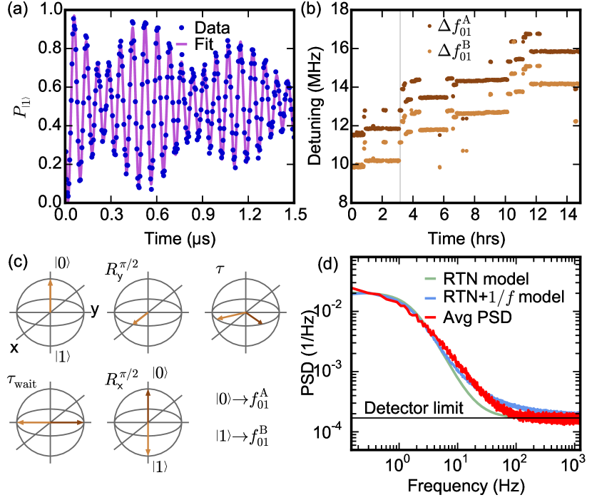
Ramsey measurements reveal a switching of from a strong coupling of charge TLSs to of the nanowire, yielding a beating pattern of two exponentially decaying sinusoids [Fig. 2(a)]. The observed frequency difference is consistent with the strong coupling of a TLS to the qubit (, the respective dephasing times). Repeating this measurement over 14 hours confirms a constant spacing between [Fig. 2(b)] with an additional drift indicating further TLSs that switch on a much slower timescale. Because is much larger than the transmon’s charge dispersion Koch et al. (2007) of only and constant over time, in contrast to Ristè et al. (2013), we conclude that the TLS couples to the nanowire . This strong TLS coupling is the reason why we do not report Ramsey coherence times () in Fig. 1. The qubit can be used to measure the state of the TLS in real time using a single-shot Ramsey-based pulse sequence tailored for [Fig. 2(c)] Ristè et al. (2013). Using the time evolution of the TLS state, we show that its double-sided power spectral density (PSD) can be explained by an asymmetric random telegraph noise (RTN) with characteristic switching times of [Fig. 2(d)], see Ref. SM, for details. Better agreement with the measured PSD is achieved by taking noise into account. The switching of between multiple values can be observed in several qubits. In addition, the frequency difference was observed to depend on the electrostatic environment of the junction for gatemons SM . This dependence indicates that the TLSs are charge traps in the vicinity of the junction that influence the transmission probabilities of the Andreev bound states.
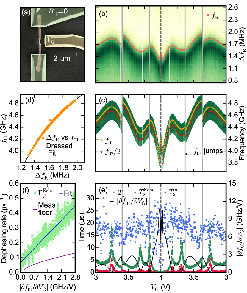
We now study the spectrum of a gatemon as a function of [Fig. 3(a-d)]. The tuning changes by altering the of the Andreev bound states, hence altering . The tuning is repeatable upon small excursions (1-2 ), except for isolated deviations which we attribute to charge traps changing state. These changes — some are reproducible, others are stochastic — lead to jumps in . Because the gatemon-resonator pair is well described by the dressed-state picture Blais et al. (2004), is easily found after a jump by measuring and calculating the expected .
For the gatemon, the dominant source of dephasing is on-chip voltage noise. A clear correlation between the sensitivity of the qubit, , and and is observed [Fig. 3(e)]. The ratio between echo and Ramsey coherence times of roughly 8 (data not shown) indicates that the white noise contribution is small Martinis et al. (2003). Therefore, only a linear fit to plotted against is performed [Fig. 3(f)] Martinis et al. (2003); Yoshihara et al. (2006); Hutchings et al. (2017); SM . The extracted quantities are a voltage-noise-independent offset of and a voltage noise amplitude , where . The extracted noise is clearly larger than the noise floor of the biasing circuit SM , indicating charge noise on the chip as the dominant source of noise. Possible origins of the dominant charge noise are the substrate or surface absorbents SM ; Gül et al. (2015).
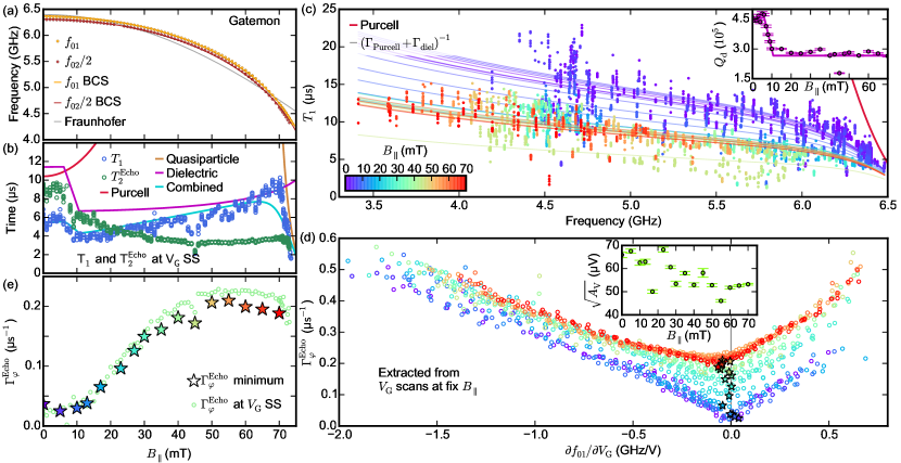
We now apply a to the same gatemon. We focus on the gatemon because flux-tunable devices experience fluctuating due to imperfect alignment and limited stability of . In order to disentangle and contributions, the gatemon is placed at the same sweet spot for each value. We directly attribute the observed monotonic decrease in with [Fig. 4(a)] to a reduction of the induced superconducting gap in the nanowire junction, Tinkham (1996). We expect the bulk of the cQED chip to exhibit little change due to the high parallel critical field () of the NbTiN film. We approximate the energy of the Andreev bound state with . The Hamiltonian is then fitted to and , fixing to the bulk Al gap and to the value obtained for the split-junction device. The best-fit agrees well with the data and yields the free parameters and . The extracted of the Al shell is in good agreement with other measurements of wires from this growth batch Chang et al. (2015). Because is not collinear with the nanowires, the of different qubits varies between and 90 , with a rough correlation to the angle between the nanowire and the direction of SM . The values stay constant over the duration of a cooldown and vary by between cooldowns, provided the sample orientation is kept fixed. A Fraunhofer type model, where the reduction of is explained by flux penetration of an extended junction Tinkham (1996), provides neither qualitative nor quantitative agreement with the data.
Finally, we investigate the coherence properties of the gatemon in . At each value, the gatemon is placed at a sweet spot and and are measured [Fig. 4(b)]. At low (high ), is limited by the Purcell effect () of the readout resonator. At high , the superconducting gap becomes so weak that quasiparticles (assumed to be at an effective temperature of 100 ) impose a limit Ristè et al. (2013). By changing , the dependence of on frequency is measured at different [Fig. 4(c)]. Heuristically, we describe the structure of the data with a dielectric model. The data for each value of are fitted with , where the -dependent dielectric quality factor is the only free parameter. The trend in shows two plateaus [Fig. 4(c) inset]; the value of decreases from for to for . Using an interpolation of yields an estimate of [Fig. 4(b)]. A similar trend can be observed for the internal quality factors () of some resonators in that field range SM . We could not find an explanation for this trend, but future experiments with resonators designed for field compatibility may help to understand it. The dip in at is reproducible but hysteretic. We do not understand its origin.
The dephasing rate shows an unexpected dependence on . Sweeps of at fixed values of [Fig. 4(d)] are performed to extract at different sensitivities. The minima of the dephasing rates increase with and do not quite coincide with the sweet spot. The absolute slopes of the dephasing rates can be different on opposite sides of . This is an unusual effect, potentially indicating that the lever arm of the side gate is comparable to the leverarm of the -dependent dominant noise source, which could be confirmed by studying further sweet spots. Interpolating the traces at each value of with two slopes allows extraction of a minimum dephasing rate and an average slope to compute . A weak decrease of [Fig. 4(d) inset] with can be observed. Direct comparison with Fig. 3 is not meaningful because the data were obtained in different cooldowns. Comparing the measured at the sweet spot to highlights that the minimal dephasing rate is obtained at finite [Fig. 4(e)]. Finding an explanation of the evolution in [Fig. 4(e)] as well as the dependence remains for future research.
In conclusion, we have characterized the coherence and noise processes of nanowire transmons at and explored the performance of a gatemon in . The frequency of the gatemon in decreases with the reduction of the induced superconducting gap in the nanowire. Coherence can be observed up to , limited by the closing of the gap. Immediate next experiments will focus on finding an explanation for the noise processes taking place at finite . By using a persistent current mode for the solenoid providing , it will also be possible to investigate the spectrum and coherence of flux-tunable split junction devices in . This could yield further insight into the microscopic origin of flux noise currently limiting coherence of flux-tunable transmons. Later, studying the temperature and behavior of the observed charge traps will lead to further understanding of their nature. Using nanowires with a thinner shell (10 ) covering two to four facets of the wire, while still inducing a hard gap, will allow operation of the qubits up to 0.5 Gazibegovic et al. (2017), reaching the relevant range for high-field applications.
Acknowledgements.
We thank A. Akhmerov, A. Geresdi, G. de Lange and M. de Moor for useful discussions, D. Thoen for depositing the NbTiN film, and R. Schouten and J. Watson for technical assistance. We acknowledge funding by Microsoft Corporation Station Q, the Dutch organization for Fundamental Research on Matter (FOM), the Netherlands Organization for Scientific Research (NWO), an ERC Synergy grant, and the Danish National Research Foundation.References
- Blais et al. (2004) A. Blais, R.-S. Huang, A. Wallraff, S. M. Girvin, and R. J. Schoelkopf, Phys. Rev. A 69, 062320 (2004).
- Wallraff et al. (2004) A. Wallraff, D. I. Schuster, A. Blais, L. Frunzio, R.-S. Huang, J. Majer, S. Kumar, S. M. Girvin, and R. J. Schoelkopf, Nature 431, 162 (2004).
- Josephson (1962) B. D. Josephson, Phys. Lett. 1, 251 (1962).
- Nakamura et al. (1999) Y. Nakamura, Y. Pashkin, and J. Tsai, Nature 398, 786 (1999).
- Barends et al. (2014) R. Barends, J. Kelly, A. Megrant, A. Veitia, D. Sank, E. Jeffrey, T. C. White, J. Mutus, A. G. Fowler, B. Campbell, Y. Chen, Z. Chen, B. Chiaro, A. Dunsworth, C. Neill, P. O’Malley, P. Roushan, A. Vainsencher, J. Wenner, A. N. Korotkov, A. N. Cleland, and J. M. Martinis, Nature 508, 500 (2014).
- Steffen et al. (2013) L. Steffen, Y. Salathe, M. Oppliger, P. Kurpiers, M. Baur, C. Lang, C. Eichler, G. Puebla-Hellmann, A. Fedorov, and A. Wallraff, Nature 500, 319 (2013).
- Jerger et al. (2016) M. Jerger, Y. Reshitnyk, M. Oppliger, A. Potočnik, M. Mondal, A. Wallraff, K. Goodenough, S. Wehner, K. Juliusson, N. K. Langford, and A. Fedorov, Nat. Commun. 7 (2016).
- Ristè et al. (2013) D. Ristè, M. Dukalski, C. A. Watson, G. de Lange, M. J. Tiggelman, Y. M. Blanter, K. W. Lehnert, R. N. Schouten, and L. DiCarlo, Nature 502, 350 (2013).
- Harris and Mapother (1968) E. P. Harris and D. Mapother, Phys. Rev. 165, 522 (1968).
- Imamoglu (2009) A. Imamoglu, Phys. Rev. Lett. 102, 083602 (2009).
- Hyart et al. (2013) T. Hyart, B. van Heck, I. C. Fulga, M. Burrello, A. R. Akhmerov, and C. W. J. Beenakker, Phys. Rev. B 88, 035121 (2013).
- Mourik et al. (2012) V. Mourik, K. Zuo, S. M. Frolov, S. R. Plissard, E. P. a. M. Bakkers, and L. P. Kouwenhoven, Science 336, 1003 (2012).
- Kosterlitz and Thouless (1973) J. M. Kosterlitz and D. J. Thouless, J. Phys. C 6, 1181 (1973).
- Andreev (1964) A. Andreev, JETP 19, 1228 (1964).
- Pillet et al. (2010) J. Pillet, C. Quay, P. Morfin, C. Bena, A. L. Yeyati, and P. Joyez, Nat. Phys. 6, 965 (2010).
- van Woerkom et al. (2017) D. J. van Woerkom, A. Proutski, B. van Heck, D. Bouman, J. I. Väyrynen, L. I. Glazman, P. Krogstrup, J. Nygård, L. P. Kouwenhoven, and A. Geresdi, Nat. Phys. (2017).
- Yokoyama et al. (2013) T. Yokoyama, M. Eto, and Y. V. Nazarov, J. Phys. Soc. Jap. 82, 054703 (2013).
- Samkharadze et al. (2016) N. Samkharadze, A. Bruno, P. Scarlino, G. Zheng, D. DiVincenzo, L. DiCarlo, and L. Vandersypen, Phys. Rev. Appl. 5, 044004 (2016).
- Popinciuc et al. (2012) M. Popinciuc, V. E. Calado, X. L. Liu, A. R. Akhmerov, T. M. Klapwijk, and L. M. Vandersypen, Phys. Rev. B 85, 205404 (2012).
- Doh et al. (2005) Y.-J. Doh, J. A. van Dam, A. L. Roest, E. P. Bakkers, L. P. Kouwenhoven, and S. De Franceschi, Science 309, 272 (2005).
- Pallecchi et al. (2008) E. Pallecchi, M. Gaaß, D. Ryndyk, and C. Strunk, Appl. Phys. Lett. 93, 072501 (2008).
- Della Rocca et al. (2007) M. Della Rocca, M. Chauvin, B. Huard, H. Pothier, D. Esteve, and C. Urbina, Phys. Rev. Lett. 99, 127005 (2007).
- Janvier et al. (2015) C. Janvier, L. Tosi, L. Bretheau, Ç. Girit, M. Stern, P. Bertet, P. Joyez, D. Vion, D. Esteve, M. Goffman, H. Pothier, and C. Urbina, Science 349, 1199 (2015).
- de Lange et al. (2015) G. de Lange, B. van Heck, A. Bruno, D. J. van Woerkom, A. Geresdi, S. R. Plissard, E. P. A. M. Bakkers, A. R. Akhmerov, and L. DiCarlo, Phys. Rev. Lett. 115, 127002 (2015).
- Larsen et al. (2015) T. W. Larsen, K. D. Petersson, F. Kuemmeth, T. S. Jespersen, P. Krogstrup, J. Nygård, and C. M. Marcus, Phys. Rev. Lett. 115, 127001 (2015).
- Casparis et al. (2016) L. Casparis, T. W. Larsen, M. S. Olsen, F. Kuemmeth, P. Krogstrup, Nygård, K. D. J. Petersson, and C. M. Marcus, Phys. Rev. Lett. 116, 150505 (2016).
- Chuang et al. (2013) S. Chuang, Q. Gao, R. Kapadia, A. C. Ford, J. Guo, and A. Javey, Nano Lett. 13, 555 (2013).
- Liu et al. (2015) Y.-Y. Liu, J. Stehlik, C. Eichler, M. Gullans, J. M. Taylor, and J. Petta, Science 347, 285 (2015).
- Koch et al. (2007) J. Koch, T. M. Yu, J. Gambetta, A. A. Houck, D. I. Schuster, J. Majer, A. Blais, M. H. Devoret, S. M. Girvin, and R. J. Schoelkopf, Phys. Rev. A 76, 042319 (2007).
- Ristè et al. (2013) D. Ristè, C. C. Bultink, M. J. Tiggelman, R. N. Schouten, K. W. Lehnert, and L. DiCarlo, Nat. Commun. 4, 1913 (2013).
- Thoen et al. (2017) D. J. Thoen, B. G. C. Bos, E. Haalebos, T. Klapwijk, J. Baselmans, and A. Endo, IEEE T. Appl. Supercon. 27, 1 (2017).
- Bos et al. (2017) B. G. C. Bos, D. J. Thoen, E. Haalebos, P. Gimbel, T. Klapwijk, J. Baselmans, and A. Endo, IEEE T. Appl. Supercon. 27, 1 (2017).
- Bruno et al. (2015) A. Bruno, G. de Lange, S. Asaad, K. L. van der Enden, N. K. Langford, and L. DiCarlo, Appl. Phys. Lett. 106, 182601 (2015).
- Chang et al. (2015) W. Chang, S. M. Albrecht, T. S. Jespersen, F. Kuemmeth, P. Krogstrup, J. Nygård, and C. M. Marcus, Nat. Nanotechnol. 10 (2015).
- Martinis et al. (2009) J. M. Martinis, M. Ansmann, and J. Aumentado, Phys. Rev. Lett. 103, 097002 (2009).
- Wang et al. (2014) C. Wang, Y. Y. Gao, I. M. Pop, U. Vool, C. Axline, T. Brecht, R. W. Heeres, L. Frunzio, M. H. Devoret, G. Catelani, L. I. Glazman, and R. J. Schoelkopf, Nat. Commun. 5, 5836 (2014).
- (37) See supplementary material.
- Itseez (2015) Itseez, “Open source computer vision library,” https://github.com/itseez/opencv (2015).
- Jerger et al. (2012) M. Jerger, S. Poletto, P. Macha, U. Hübner, E. Il’ichev, and A. V. Ustinov, Appl. Phys. Lett. 101, 042604 (2012).
- Motzoi et al. (2009) F. Motzoi, J. M. Gambetta, P. Rebentrost, and F. K. Wilhelm, Phys. Rev. Lett. 103, 110501 (2009).
- Martinis et al. (2003) J. M. Martinis, S. Nam, J. Aumentado, K. M. Lang, and C. Urbina, Phys. Rev. B 67, 094510 (2003).
- Yoshihara et al. (2006) F. Yoshihara, K. Harrabi, A. O. Niskanen, Y. Nakamura, and J. S. Tsai, Phys. Rev. Lett. 97, 167001 (2006).
- Hutchings et al. (2017) M. Hutchings, J. B. Hertzberg, Y. Liu, N. T. Bronn, G. A. Keefe, M. Brink, J. M. Chow, and B. Plourde, Phys. Rev. Appl. 8, 044003 (2017).
- Gül et al. (2015) Ö. Gül, D. J. Van Woerkom, I. van Weperen, D. Car, S. R. Plissard, E. P. Bakkers, and L. P. Kouwenhoven, Nanotechnology 26, 215202 (2015).
- Tinkham (1996) M. Tinkham, Introduction to Superconductivity, 2nd ed. (McGraw-Hill, New York, 1996).
- Gazibegovic et al. (2017) S. Gazibegovic, D. Car, H. Zhang, S. C. Balk, J. A. Logan, M. W. de Moor, M. C. Cassidy, R. Schmits, D. Xu, G. Wang, P. Krogstrup, R. L. M. Op het Veld, K. Zuo, Y. Vos, J. Shen, D. Bouman, B. Shojaei, D. Pennachio, J. S. Lee, P. J. van Veldhoven, S. Koelling, M. A. Verheijen, L. P. Kouwenhoven, C. J. Palmstrøm, and E. P. A. M. Bakkers, Nature 548, 434 (2017).
I Supplementary Material for “Evolution of Nanowire Transmons and Their Quantum Coherence in Magnetic Field”
This supplement provides experimental details and additional data supporting the claims in the main text.
II Experimental Setup
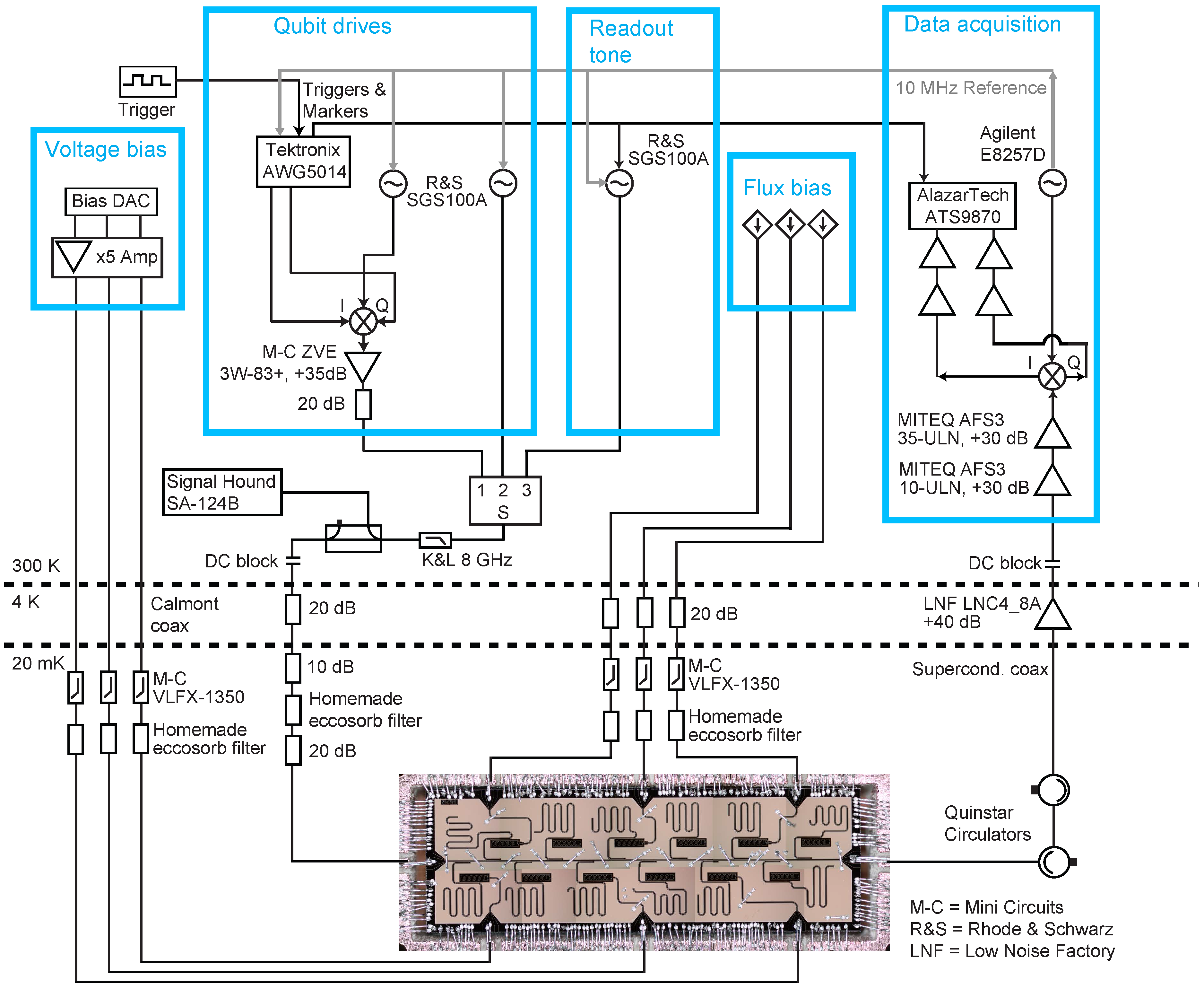
Measurements were performed in a variety of experimental conditions, differing in degrees of magnetic and radiation shielding. The data shown in Figs. 1, 2 and S3 are taken with the sample in a box that provides radiation and magnetic shielding. The shielding consists of two layers of Cryophy, a superconducting Al shield and a copper cup coated on the inside with a mixture of silicon carbide and Stycast for infrared shielding Barends et al. (2011). The data in other figures are taken with the sample in a copper box, only surrounded by a copper shield coated with the mixture. Using superconducting shields or passive magnetic shielding was not possible in this situation as this would conflict with the external magnetic field applied. The coaxial cables carrying voltages, currents and microwave signals are connected to the chip that is mounted on a printed circuit board (PCB) using non-magnetic SMP connectors. The detailed microwave setup is shown in Fig. S1. Care was taken to only use non-magnetic brass screws in proximity to sample and solenoid.
The magnetic field is generated by a single-axis, cryogen-free, compensated solenoid (American Magnetics, Inc.) with a current-to-field conversion factor 51.6 (max. 2 ), driven by a Keithley 2200-20-5 programmable power supply. This solenoid does not have a persistent current switch.
The dc current for flux biasing the split-junction devices is provided by home-built low-noise current sources mounted in a TU Delft IVVI-DAC2 rack. The voltage to bias the gatemons (provided by DACs of the IVVI rack, amplified with a 5 battery-driven amplifier) is low-pass filtered (through Calmont coaxial cables, cutoff frequency 100 , Mini Circuits VLFX 1050 and a home-made, absorptive eccosorb filter) before arriving at the sample.
Microwave tones for qubit control and readout are generated, modulated and combined at room temperature. They are coupled to the chip through the common feedline. Filtering and attenuation at different temperature stages (see Fig. S1) suppresses unwanted photon population in the readout resonators. The readout line wiring is similar to Asaad et al. (2016).
III Fabrication Procedure
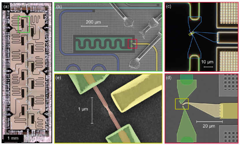
Standard cQED fabrication techniques are used to pattern ground plane, coplanar waveguide structures and qubit capacitor islands Bruno et al. (2015). Then, the NWs are deterministically placed in each qubit junction area using a nanomanipulator. The InAs NWs have an epitaxially grown Al shell Krogstrup et al. (2015); Chang et al. (2015) (core diameter 65 , shell thickness 30 ). Using a PMMA etch mask, a 200 window is etched into the Al shell. This defines the N section of the SNS junction. The wet etchant used (Transene D, 12 at 50 ) is selective enough that no damage to the InAs core can be detected in scanning electron microscope (SEM) micrographs [Fig. S2(e)]. Some SEM micrographs reveal residues of Al in the junction area of the NWs. We could not establish a correlation between qubit or and such residues.
To contact the Al shell, a gentle in-situ argon plasma etch is first used to remove the aluminum oxide. Then, the NbTiN contacts to capacitor plates and sidegates are sputtered.
On-chip Al wirebonds are used to suppress slot-line modes. These are added as the sample is also wirebonded to a standard PCB.
| Setup | Qubit | [∘] | Comment | |||||
| Mag. Shields | C | 6.08 | 7.08 | 15-20 | 15-20 | - | - | 2 freqs, 10-15 , Single |
| H | 6.618 | 6.815 | 7-10 | 6-8 | - | - | Single-junction, ungated | |
| J | 6.832 | 4.9 (SS) | 10-20 | 30 (SS) | - | - | Flux-tunable, Figs. 1, 2 | |
| K | 6.93 | 5.68 | 2.5-3 | 1.7-2.1 | - | - | Single-junction, ungated | |
| Mag. Shields | 1 | 6.41 | 7.62 | 5-5 | 1 | - | - | Gatemon |
| 4 | 6.20 | 4.48 | 7-10 | 4 | - | - | Single-junction, ungated | |
| 5 | 6.30 | 5.4-5.8 | 4-7 | 1-2 | - | - | Gatemon, Fig. S3 | |
| 6 | 6.42 | 7.62 (SS) | 4-5 | 1 (SS) | - | - | Flux tunable | |
| SolenoidShield | 1 | 5.88 | 7.06 | 7 | 2 | - | 15 | Gatemon |
| 4 | 6.21 | 5.49 | 4.5 | 4 | 60/59/60 | 50 | Single-junction, ungated | |
| 5 | 6.31 | 5.08 | 3-4 | 2-3 | 53 | 60 | Gatemon | |
| 6 | 6.42 | 7.22 | 6-10 | 8 (SS) | 95/95 | 5 | Flux tunable | |
| 9 | 6.74 | 4-6.5 | 10-30 | 20 (SS) | 86/82 | 10 | Gatemon, Figs. 3, 4, S4 |
IV Image Recognition Software
The advantage of top-down fabrication common in cQED is compromised for NW transmons: a bottom-up fabrication approach is required for individual NWs. Each NW has a different position with respect to the corresponding qubit leads, hence etch mask and contacts (including sidegate) must be individually designed for each qubit. To reduce the turnaround time, we wrote software to automatically generate these masks using optical dark field images [compare Fig. S2(c)] Itseez (2015).
Our image recognition software employs a suite of filtering procedures and feature detection algorithms to reliably design etch and contact masks. First, the image is low-pass filtered with a Gaussian point spread function. This reduces the sensitivity to possible dirt in the junction area. The image is then binarised using Otsu’s thresholding method Otsu (1979). To further reduce the chance of picking up uninteresting features (such as the holes in the ground plane) and increase the stability of the procedure, a morphological filter combines adjacent areas Serra (1997). The Canny edge detection algorithm finds all contours present in the image. These are compared to the known shape of the leads to select the best match (green) Canny (1986). The scaling, rotation and offset of the image are determined using a Hough transformation and fitting the analytical shape of the leads to the extracted contours (red) Ballard (1981). This allows the definition of a coordinate system. The NW is then determined as the contour between the leads enclosing the largest area. The orientation and position of the NW are determined by the smallest rectangle encompassing the NW contour. This allows correct detection of the NW in of the cases. The position and orientation information is used to create the pattern file for the etch windows (yellow), and to place and connect (light blue) contacting regions predefined with respect to leads and wire using a distance minimizing routine. These contours are used to generate the pattern file for the contact mask.
The performance of the image recognition software is sufficient for our purpose. The NW width is only 130 , well below the diffraction limit (500 ) and the effective width of the wire in the image ( ). The achieved rms error in sidegate placement is 140 .
V Gatemon Frequency Switching
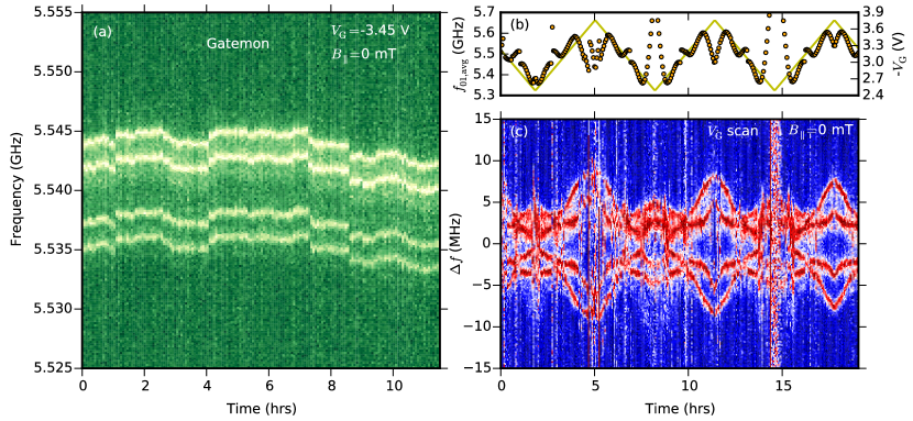
We have observed the switching of the qubit transition frequency due to strongly coupled TLSs influencing also in gatemons. Figure S3(a) shows repeated pulsed spectroscopy scans taken at fixed . Four distinct, drifting values of with semi-constant spacings are clearly visible. A possible explanation of the four frequencies is the strong coupling of two TLSs to . A background of many weakly coupled TLSs causes the drift in the center frequency.
The difference between the values of depends on the applied [Figs. S3(b,c)]. Pulsed spectroscopy scans are performed while is swept up and down. For each scan, the multiple values of are extracted and their average is set to . The frequency spacing between the peaks changes with . We therefore interpret the -sensitive TLSs that are influencing to be charge traps in the vicinity of the NW junction. The frequencies do not return to the same value upon return to the same . The drift of the center frequency made it challenging to setup a reliable frequency state measurement (compare Fig. 2). Hence, we were not able to estimate the PSD of these TLSs.
VI PSD of the TLS
The strong coupling of a TLS to the flux-tunable, split junction qubit [Fig. 2(a,b)] allows detailed characterization of the TLS dynamics in real time via Ramsey based time-domain measurements [Fig. 2(c,d)] Ristè et al. (2013). By monitoring the frequency state of the qubit every for 6.6 , we track the TLS state over time. The PSDs of such traces, given as
| (S1) |
are averaged to get an estimation of the TLS PSD. The TLS PSD can be approximated by an asymmetric random telegraph noise (RTN) model
| (S2) |
where and are the two switching rates and is the detector fidelity [Fig. 2(d)].
Better agreement with the observed data can be achieved by taking the influence of noise into account [Fig. 2(d)]. Given the switching rates , the noise-free TLS traces are simulated using a Markov chain approach. Subsequently, frequency noise that is generated by spectrally filtering white noise is superimposed on the TLS traces. The action of the Ramsey experiment with evolution time is thresholded to obtain the detector signal at the -th time step, at which the frequency of the TLS is . The detector fidelity (defined as , where are the detection error probabilities for the and states) is taken into account by probabilistically flipping the thresholded values. PSDs of many such traces are calculated using Eq. (S1) and their average is compared to the experimental PSD. The experimental parameters of difference , and are used for the simulations. Switching rates and and fidelity agree well with the values found with the asymmetric RTN model [Eq. (S2)]. The additional noise has an amplitude at 1 . The resulting PSD matches the experimentally obtained PSD better than just an asymmetric RTN curve. This suggests that noise plays an important role.
VII Noise PSD extraction from dephasing rates
The qubits can be used to probe the noise on the control knobs they are sensitive to. In the presence of noise in , the increases with increasing sensitivity to , . By performing a quadratic fit,
| (S3) |
we can extract the relevant noise parameters Martinis et al. (2003); Yoshihara et al. (2006); Hutchings et al. (2017). These are the -independent offset , a noise contribution linear in and a white noise contribution quadratic in . We quantify the PSD by
| (S4) |
The white noise is quantified by
Using the qubits as detectors to measure the noise they are subjected to therefore reveals information about the direct environment of the qubits (Figs. 1 and 3). This is needed to exclude that our control electronics limits the performance of the qubits (Fig. S4).
VIII Coherence limitation given a noise PSD
It is also possible to measure the noise generated by the control electronics and from that calculate a limit on the qubit dephasing time Martinis et al. (2003). To do so, the PSD of is measured at room temperature. The induced mean-squared phase-noise at a time is then given as
| (S5) |
where is the filter function of the echo sequence used Martinis et al. (2003),
| (S6) |
Under the assumption of Gaussian noise, the expected measurement outcome in the computational basis can be expressed as
| (S7) | ||||
Inserting the measured PSD and the appropriate filter function [Eq. (S6)] into Eq. (S5) allows us to compute the echo time, using Eq. (S7). This provides a tool to calculate an upper limit on the dephasing rates due to the setup.
IX Voltage noise
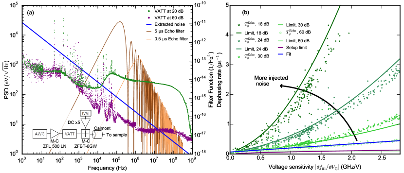
The procedure described above to calculate the dephasing limit is verified on a gatemon, where additional noise is injected to be the dominating dephasing contribution (Fig. S4). Noise is generated by amplifying the 0-output of a Tektronix AWG 5014 with a Mini-Circuits ZFL 500 LN amplifier. Its amplitude is controlled by a Weinschel Aeroflex 8320 variable attenuator (VATT). The noise is injected to the DC biasing circuit using a Mini-Circuits ZFBT-6GW bias tee [inset Fig. S4(a)]. The noise PSDs for the VATT at 60 dB attenuation (no added noise) and at 20 dB (added noise dominates) are measured with a SRS SR770 FFT network analyzer in the range . The range between and is measured with a Rigol DSA 815 spectrum analyzer [Fig. S4(a)]. The PSDs are measured after the bias tee, and the transfer function correction of the Calmont coaxial line is applied to the measured spectra. Note that the noise level measured for the VATT at 60 dB is not discernible from the instrument background. Hence, this only gives an upper limit to the noise floor. In Fig. S4(b), dephasing rates for different noise levels are plotted and compared to the expected rates given the rescaled injected noise using Eq. (S7). In the cases where the injected noise is dominant the agreement is good. A strong deviation becomes apparent when no noise is injected. This indicates the presence of another noise source. The extracted noise from that source [Eq. (S4), Figs. S4(a) and 3(f)] exceeds the upper limit on the setup noise floor.
X Noise in
An accurate estimation of the dephasing time limit imposed by noise in is not possible due to the large inductance of the magnet. Although the current noise of the solenoid biasing circuit was measured, a reliable conversion into an effective noise in is not straightforward. This is because the (frequency-dependent) conversion function of current to field is not known. However, the solenoid acts as a large low-pass filter. Therefore it is unlikely that this source of noise limits the observed dephasing times.
XI Resonator performance in
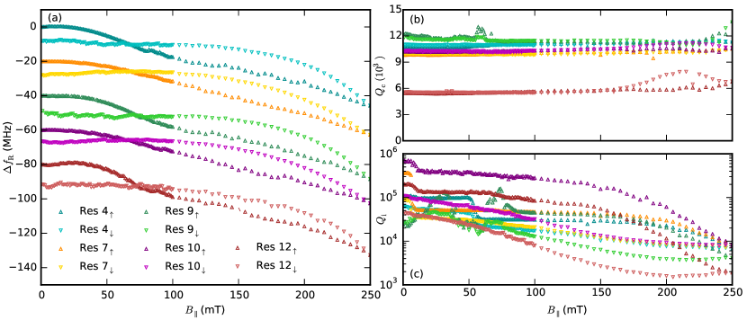
The fundamental frequency and the internal quality factor of the resonators change with applied magnetic field due to the changing kinetic inductance and the induction of vortices in the film. An increase in means a decrease of the Cooper pair density in the superconducting film, leading to a higher kinetic inductance and thus decreasing . This effect can be seen in Fig. S5(a), showing the deviation from the zero-field of several resonators against . Upon return to zero field, this contribution alone does not lead to a hysteretic effect. Hysteretic effects can arise from a net magnetization of the film producing a change in the current distribution of the resonator mode Bothner et al. (2012). Vortices induced in the film will experience a Lorentz force due to the current in the resonator, causing them to dissipatively move around, lowering . The values of are extracted using real and imaginary part of the feedline transmission Bruno et al. (2015). To speed up measurements, an average intraresonator photon number of was used. In several of the resonators, a decrease in between 6 and 10 can be observed. This is in qualitative agreement with the observed decrease in in this field range [Fig. 4(c), inset]. Besides this decrease, the performance of the resonators up to 70 allows to perform the experiments presented.
References
- Barends et al. (2011) R. Barends, J. Wenner, M. Lenander, Y. Chen, R. C. Bialczak, J. Kelly, E. Lucero, P. O’Malley, M. Mariantoni, D. Sank, H. Wang, T. C. White, Y. Yin, J. Zhao, A. N. Cleland, J. M. Martinis, and J. J. A. Baselmans, Appl. Phys. Lett. 99, 113507 (2011).
- Asaad et al. (2016) S. Asaad, C. Dickel, S. Poletto, A. Bruno, N. K. Langford, M. A. Rol, D. Deurloo, and L. DiCarlo, npj Quantum Inf. 2, 16029 (2016).
- Bruno et al. (2015) A. Bruno, G. de Lange, S. Asaad, K. L. van der Enden, N. K. Langford, and L. DiCarlo, Appl. Phys. Lett. 106, 182601 (2015).
- Krogstrup et al. (2015) P. Krogstrup, N. L. B. Ziino, W. Chang, S. M. Albrecht, M. H. Madsen, E. Johnson, J. Nygård, C. M. Marcus, and T. S. Jespersen, Nat. Mater. 14 (2015).
- Chang et al. (2015) W. Chang, S. M. Albrecht, T. S. Jespersen, F. Kuemmeth, P. Krogstrup, J. Nygård, and C. M. Marcus, Nat. Nanotechnol. 10 (2015).
- Gül et al. (2015) Ö. Gül, D. J. Van Woerkom, I. van Weperen, D. Car, S. R. Plissard, E. P. Bakkers, and L. P. Kouwenhoven, Nanotechnology 26, 215202 (2015).
- Itseez (2015) Itseez, “Open source computer vision library,” https://github.com/itseez/opencv (2015).
- Otsu (1979) N. Otsu, IEEE T. Sys. Man and Cyb. 9, 62 (1979).
- Serra (1997) J. Serra, Image Analysis & Mathematical Morphology (Academic Press, 1997).
- Canny (1986) J. Canny, IEEE T. PAMI 8, 679 (1986).
- Ballard (1981) D. H. Ballard, Pattern recognition 13, 111 (1981).
- Ristè et al. (2013) D. Ristè, C. C. Bultink, M. J. Tiggelman, R. N. Schouten, K. W. Lehnert, and L. DiCarlo, Nat. Commun. 4, 1913 (2013).
- Martinis et al. (2003) J. M. Martinis, S. Nam, J. Aumentado, K. M. Lang, and C. Urbina, Phys. Rev. B 67, 094510 (2003).
- Yoshihara et al. (2006) F. Yoshihara, K. Harrabi, A. O. Niskanen, Y. Nakamura, and J. S. Tsai, Phys. Rev. Lett. 97, 167001 (2006).
- Hutchings et al. (2017) M. Hutchings, J. B. Hertzberg, Y. Liu, N. T. Bronn, G. A. Keefe, M. Brink, J. M. Chow, and B. Plourde, Phys. Rev. Appl. 8, 044003 (2017).
- Bothner et al. (2012) D. Bothner, T. Gaber, M. Kemmler, D. Koelle, R. Kleiner, S. Wünsch, and M. Siegel, Phys. Rev. B 86, 014517 (2012).