Local Real-Space View of the Achiral 1-TiSe2 2 2 2 Charge Density Wave
Abstract
The transition metal dichalcogenide 1-TiSe2 is a quasi-two-dimensional layered material undergoing a commensurate 2 2 2 charge density wave (CDW) transition with a weak periodic lattice distortion (PLD) below 200 K. Scanning tunneling microscopy (STM) combined with intentionally introduced interstitial Ti atoms allows to go beyond the usual spatial resolution of STM and to intimately probe the three-dimensional character of the PLD. Furthermore, the inversion-symmetric, achiral nature of the CDW in the -direction is revealed, contradicting the claimed existence of helical CDW stacking and associated chiral order. This study paves the way to a simultaneous real-space probing of both charge and structural reconstructions in CDW compounds.
Transition metal dichalcogenides (TMDCs) have been extensively studied for decades, but recently, the development of methods to obtain nanosheets or even monolayers has brought renewed interest for these materials because of their attractive electronic and optoelectronic properties for applications Chhowalla et al. (2013); Wang et al. (2012). Many TMDCs also undergo charge density waves (CDW) or/and superconducting phase transitions at low temperature Withers and Wilson (1986); Castro Neto (2001); Fang et al. (2005); Chatterjee et al. (2015); Joe et al. (2014) and recently, 1-TiSe2 has been even proposed as the first TMDC exhibiting a CDW with a scalar chiral order Ishioka et al. (2010); Castellan et al. (2013).
Scanning tunneling microscopy (STM) probes the real-space surface electron density. Therefore, the electronic reconstruction associated with the commensurate 2 2 2 CDW of 1-TiSe2 can be easily tracked in the topmost Se layer up to atomic resolution Slough et al. (1988); Novello et al. (2015). This local approach has indeed allowed to propose the chirality of the CDW Ishioka et al. (2010); Iavarone et al. (2012) and to observe the formation of phase-shifted CDW domains induced by intercalation of Ti or Cu atomsHildebrand et al. (2016); Yan et al. (2017); Hildebrand et al. (2017); Novello et al. (2017). However, the three-dimensional (3D) character of the CDW as well as the periodic lattice distortion (PLD) accompanying the phase transition can, in principle, not be directly probed, the displacement amplitude induced by the PLD Di Salvo et al. (1976); Fang et al. (2017) being well below the usual spatial resolution of STM Chen (2008).
Yet, being able to obtain information about the 3D character of the CDW as well as getting insight about the PLD in real-space is of fundamental interest in the context of domain formation or CDW dimensional crossover Chen et al. (2016), but also with respect to the question of chirality which strictly signifies a loss of inversion symmetry between two adjacent Se-Ti-Se sandwiches.
Here, the electronic signature of defects induced by the presence of interstitial Ti atoms in-between Se-Ti-Se sandwiches is exploited for probing the symmetry of the PLD. This combined STM-defect technique therefore goes beyond the resolution limitation of STM providing access to the structural and intimate 3D nature of the 1-TiSe2 CDW. Interstitial Ti defects are first recognized and characterized. A systematic asymmetry induced by the surrounding surface PLD is observed and the associated deformation is uniquely determined with the help of density functional theory (DFT) calculations. Furthermore, the potential of this new technique is highlighted through a simultaneous measurement of two adjacent Se-Ti-Se sandwiches at a step edge where the CDW/PLD is found to display the expected commensurate 2 2 2 signature with atomic displacements as proposed by Di Salvo et al. Di Salvo et al. (1976). Therefore, there is no evidence of a loss of inversion symmetry, contradicting recent claims of a chiral phase Ishioka et al. (2010); Iavarone et al. (2012).
The strength of this combined STM-defect technique also relies on its relative simplicity. Indeed, a defect density of less than 1 allows precise identification of the surface PLD. Hence, this work not only paves the way towards a better local understanding of structural reconstructions in CDW compounds but is also highly promising for phase transition studies in general, where a local and real-space vision of entangled electronic and structural instabilities is essential.
The 1-TiSe2 single crystals were grown by iodine vapor transport at 700 \celsius with 5 additional Ti in the growth tube with respect to perfect stoichiometric conditions. Resistivity measurements were performed by a standard four-probe method using a lock-in as current source and voltage meter. The samples were cleaved in-situ below 10-7 mbar at room temperature. Constant current STM images were recorded at 4.6 K using an Omicron LT-STM, with bias voltage V applied to the sample. Base pressure was better than 510-11 mbar.
DFT calculations have been performed using the plane-wave pseudopotential code VASP Kresse and Hafner (1993); Kresse and Furthmüller (1996), version 5.3.3. Projector augmented waves Kresse and Joubert (1999) were used with the Perdew-Burke-Ernzerhof (PBE) Perdew et al. (1996) exchange correlation functional. The cell size of our model was 28.035 Å 28.035 Å. The 1-TiSe2 surface was modeled with two layers and the bottom Se layer fixed. A Monkhorst-Pack mesh with 2 2 1 points was used to sample the Brillouin zone of the cell. The parameters gave an energy difference convergence of better than 0.01 eV. During structural relaxations, a tolerance of 0.03 eV/Å was applied. STM images were generated using the Tersoff-Hamann approach Tersoff and Hamann (1983) in which the current measured in STM is proportional to the integrated LDOS of the surface using the bSKAN code Hofer (2003).

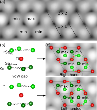
Figure 1 (a) shows a DFT simulation, relaxed from displacements following Di Salvo et al. Di Salvo et al. (1976), of a high-resolution low-temperature empty-state STM image of 1-TiSe2 close to (small positive ) Novello et al. (2015). In addition to the 1 1 charge density corresponding to the position of the atoms in the topmost Se layer Slough et al. (1988), the 2 2 CDW modulation can be identified through the succession of atoms appearing more or less intense and labeled CDW max. [see max in Fig. 1 (a)] and CDW min [see min in Fig. 1 (a)]. The 2 2 surface unit cell contains exactly one CDW max. and three CDW min. [dashed rhombus in Fig. 1 (a)]. In-plane displacement amplitude of the Se atoms [see Se and Se in Fig. 1 (b)] corresponds to 0.028 Å at 77 K Di Salvo et al. (1976) which is almost two orders of magnitude below the highest lateral resolution reached by standard STM and can thus not be directly tracked with this technique. Interestingly, according to the PLD, the new unit cell also contains exactly one Se atom which has not moved with respect to its normal state position and three Se which have undergone a small distortion. This observation demonstrates the close relationship between CDW modulation and PLD and allows to directly associate the CDW max. to the non-displaced Se atoms [see Se max. atoms in Fig. 1 (c)] and the CDW min. to the displaced ones [see arrows on Se min. atoms in Fig. 1 (c)].
Nevertheless, we would like to stress that, measuring the 2 2 charge modulation with STM does not allow to uniquely determine the handedness of the PLD occuring within the first Se-Ti-Se sandwich. Indeed, due to the characteristic antiphase locking of the 2 2 2 CDW between adjacent Se-Ti-Se layers [see Fig. 1 (b) and (c)] Di Salvo et al. (1976), there are two possible periodic distortions [right-handed or left-handed, see Fig. 1 (c)] for one CDW modulation at the surface. STM alone is therefore completely blind to this essential parameter exhibiting the 3D character of the CDW.

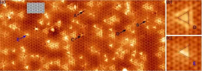
Figure 2 (a) displays a measured large empty-state STM image close to (150 mV). Many types of atomic defects can be recognized, the overall impurity density approximately corresponding to 2. A large proportion of defects are the well-known native impurities described in a previous study Hildebrand et al. (2014). Defect A corresponds to a Se vacancy, defects B and C are Se substitutions by iodine and oxygen atoms, respectively, and defect D is associated to intercalated Ti in the vdW gap. Based on surveys from STM images obtained at different regions of the sample (not shown), the density of intercalated Ti defects which is mostly determined by the growth temperature (700 \celsius) Di Salvo et al. (1976), is 0.570.07 and has therefore no impact on the CDW long-range phase coherence as seen Fig. 2 (a) Hildebrand et al. (2016).
In addition to these four native impurities, the non-stoichiometric growth conditions have introduced another defect, never observed previously Hildebrand et al. (2014); Novello et al. (2015). It stands out from the periodic and ordered Se layer as small, bright asymmetric triangle [defect E, Fig. 2 (a)]. The estimated density of defect E is 0.790.08, a value close to the density of intercalated Ti [defect D, Fig. 2 (a)]. It should not be confused with the latter, which also presents a very similar small triangular shape due to enhanced density of states on top of the three neighboring Se atoms in filled-states Hildebrand et al. (2014), below -0.2 V. One has to keep in mind that at this bias voltage (0.15 V), i.e. in empty-states, the electronic perturbation induced by intercalated Ti is spatially much more extended, in such a way that the difference between defect D and E is manifest [see zooms-in on both defects in Fig. 2 (b) and (c) for comparison]. Figure 2 (c) also allows us to highlight the particular asymmetric nature of the electronic signature of defect E with respect to the lattice. Indeed, two of the three topmost Se atoms concerned with its electronic perturbation are clearly brighter than the third one building a ”bright edge”.
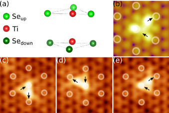
Given the special growth conditions, defect E can be reasonably attributed to additional Ti atoms. Also, the orientation of the triangular shape of defect E is identical to the central triangle of the intercalated-Ti electronic signature [see small dotted triangles Fig. 2 (b) and (c)]. This indicates that, as intercalated Ti, defect E is in vertical alignment with a structural Ti atom. Therefore, we performed DFT simulations of STM images in the 2 2 2 phase with an interstitial Ti atom located inside a TiSe6 octahedron forming a Ti2Se6 structure [Fig. 3 (a))]. As seen in Fig. 3 (b), the DFT-simulated image for the relaxed structure at 150 mV of is in excellent agreement with our measurement and especially accounts for the characteristic bright edge. The arrows give the direction of displacements of the top Se atoms according to the PLD introduced in the simulation.

In particular, one of the atoms building the bright edge is a CDW max. (non-displaced atom) and the second bright atom corresponds to an atom which moves away from the first one according to the PLD. Comparing the simulation to the three observed conformations of the bright edge induced by interstitial Ti atoms in Fig. 2 [see zoom-ins in Fig. 3 (c)-(e)] first confirms that it is always constituted of one CDW max. 111Interstitial Ti atoms can also be situated in such a way that the three atoms composing its triangular shape are three min. of the CDW modulation. Even though, a detailed analysis of this conformation has been done, it is not presented here since the measurement as well as the calculation show that, for this specific case, the asymmetry is only weak and not well defined due to the perfectly symmetric nature of its position with respect to the CDW/PLD. Hence, in this position with respect to the lattice, interstial Ti can not be used as a probe of the PLD. For more precisions about the PLD-induced inequivalent conformations of single-atom defects see Refs.Novello et al. (2015); Hildebrand et al. (2017).. Then, plotting the corresponding directions of distortion on the observed conformations [arrows Fig. 3 (c)-(e)] uniquely demonstrates that, here, the underlying PLD is the left-handed one [Fig. 1 (c)].

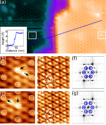
One has to realize that one single interstitial-Ti atom defect on a STM image is already sufficient for probing the orientation of the underlying PLD ensuring, in turn, that the 3D character of the CDW can be probed through this novel method with minimal defect-induced disturbance. Figure 4 (a) shows an STM image at a step edge between two adjacent layers separated by Å corresponding to one lattice constant [see inset of Fig. 4 (a)]. The CDW charge modulation is recognizable on both terraces and can be easily tracked. Also, two interstitial-Ti defects are clearly observable on each side of the step edge [see white rectangles in Fig. 4 (a)] therefore providing atomic probes of the PLD orientation for the top and bottom TiSe2 layers. Comparing the positions of the CDW maxima with the electronic signatures of the interstitial-Ti atoms for both layers [see white circles on zooms-in Fig. 4 (b) and (c)] allows for determining the direction of motion that the Se atoms have undergone through the phase transition [see black arrows in Fig. 4 (b) and (c)]. The PLD is therefore found to be left-handed for the top layer and right-handed for the bottom [Fig. 1 (c)], demonstrating that we are facing a local real-space view of the 2 2 2 character of the 1-TiSe2 CDW.
Furthermore, our experiment allows to readily conclude on the inversion-symmetric achiral nature of the CDW as initially proposed by Di Salvo et al. Di Salvo et al. (1976). Indeed, the recently claimed chirality of the 1-TiSe2 CDW is based on a helical stacking of the three CDW -vectors along the -direction with a 2/3 interval, leading to the existence of so-called virtual layers with shifted CDW density peaks Ishioka et al. (2010). This implies different amplitudes of CDW charge modulations along the three -vectors not only in a single layer but also between two -separated TiSe2 layers. Two identically sized defect-free regions of both layers are selected in Fig. 4 (a) and shown in Fig. 4 (d) and (e). Their close similarity in real-space already suggest that no relative phase shifts exist between the three CDW -vectors. In addition, the integrated intensities of the CDW extra-spots on fast-Fourier transformed (FFT) images obtained from Fig. 4 (d) and (e) [Fig. 4 (f) and (g)] show a negligible variation of less than 5. This definitely confirms the conventional layer stacking in 1-TiSe2 and rules out the proposed 2/3 helical CDW stacking of chiral CDW phases Ishioka et al. (2010).
In summary, the combination of STM with a low-density of specific buried defects has been used to uncover the periodic lattice distortion at the 1-TiSe2 surface. The potential of this new PLD-sensitive probe has been then exemplified through the measurement of the inversion of its handedness at a step edge therefore providing a real-space view of the 2 2 2 character of the CDW. The inversion-symmetric nature of the CDW in the -direction has been finally confirmed, contradicting the existence of CDW helical stacking and associated chiral order. In principle, this new method could be easily extended to the analysis of the mixed CDW-superconducting state in Cu-intercalated 1-TiSe2 Yan et al. (2017), as well as to other materials exhibiting phase transitions for which a better understanding of the interplay between electronic and structural degrees of freedom is required.
Acknowledgements.
This project was supported by the Fonds National Suisse pour la Recherche Scientifique through Div. II. We would like to thank C. Monney, C. Renner and M. Spera for motivating discussions. Skillful technical assistance was provided by F. Bourqui, B. Hediger and O. Raetzo. B.H. and T.J. equally contributed to this work.References
- Chhowalla et al. (2013) M. Chhowalla, H. S. Shin, G. Eda, L.-J. Li, K. P. Loh, and H. Zhang, Nat. Chem. 5, 263 (2013).
- Wang et al. (2012) Q. H. Wang, K. Kalantar-Zadeh, A. Kis, J. N. Coleman, and M. S. Strano, Nat. Nanotechnol. 7, 699 (2012).
- Withers and Wilson (1986) R. L. Withers and J. A. Wilson, J. Phys. C Solid State Phys. 19, 4809 (1986).
- Castro Neto (2001) A. H. Castro Neto, Phys. Rev. Lett. 86, 4382 (2001).
- Fang et al. (2005) L. Fang, P. Zou, Y. Wang, L. Tang, Z. Xu, H. Chen, C. Dong, L. Shan, and H. Wen, Sci. Technol. Adv. Mater. 6, 736 (2005).
- Chatterjee et al. (2015) U. Chatterjee, J. Zhao, M. Iavarone, R. Di Capua, J. P. Castellan, G. Karapetrov, C. D. Malliakas, M. G. Kanatzidis, H. Claus, J. P. C. Ruff, F. Weber, J. van Wezel, J. C. Campuzano, R. Osborn, M. Randeria, N. Trivedi, M. R. Norman, and S. Rosenkranz, Nat. Commun. 6, 6313 (2015).
- Joe et al. (2014) Y. I. Joe, X. M. Chen, P. Ghaemi, K. D. Finkelstein, G. A. de la Peña, Y. Gan, J. C. T. Lee, S. Yuan, J. Geck, G. J. MacDougall, T. C. Chiang, S. L. Cooper, E. Fradkin, and P. Abbamonte, Nat. Phys. 10, 421 (2014).
- Ishioka et al. (2010) J. Ishioka, Y. H. Liu, K. Shimatake, T. Kurosawa, K. Ichimura, Y. Toda, M. Oda, and S. Tanda, Phys. Rev. Lett. 105, 176401 (2010).
- Castellan et al. (2013) J.-P. Castellan, S. Rosenkranz, R. Osborn, Q. Li, K. E. Gray, X. Luo, U. Welp, G. Karapetrov, J. P. C. Ruff, and J. van Wezel, Phys. Rev. Lett. 110, 196404 (2013).
- Slough et al. (1988) C. G. Slough, B. Giambattista, A. Johnson, W. W. McNairy, C. Wang, and R. V. Coleman, Phys. Rev. B 37, 6571 (1988).
- Novello et al. (2015) A. M. Novello, B. Hildebrand, A. Scarfato, C. Didiot, G. Monney, A. Ubaldini, H. Berger, D. R. Bowler, P. Aebi, and C. Renner, Phys. Rev. B 92, 081101(R) (2015).
- Iavarone et al. (2012) M. Iavarone, R. Di Capua, X. Zhang, M. Golalikhani, S. A. Moore, and G. Karapetrov, Phys. Rev. B 85, 155103 (2012).
- Hildebrand et al. (2016) B. Hildebrand, T. Jaouen, C. Didiot, E. Razzoli, G. Monney, M.-L. Mottas, A. Ubaldini, H. Berger, C. Barreteau, H. Beck, D. R. Bowler, and P. Aebi, Phys. Rev. B 93, 125140 (2016).
- Yan et al. (2017) S. Yan, D. Iaia, E. Morosan, E. Fradkin, P. Abbamonte, and V. Madhavan, Phys. Rev. Lett. 118, 106405 (2017).
- Hildebrand et al. (2017) B. Hildebrand, T. Jaouen, C. Didiot, E. Razzoli, G. Monney, M.-L. Mottas, F. Vanini, C. Barreteau, A. Ubaldini, E. Giannini, H. Berger, D. R. Bowler, and P. Aebi, Phys. Rev. B 95, 081104 (2017).
- Novello et al. (2017) A. M. Novello, M. Spera, A. Scarfato, A. Ubaldini, E. Giannini, D. R. Bowler, and C. Renner, Phys. Rev. Lett. 118, 017002 (2017).
- Di Salvo et al. (1976) F. Di Salvo, D. Moncton, and J. Waszczak, Phys. Rev. B 14, 4321 (1976).
- Fang et al. (2017) X.-Y. Fang, H. Hong, P. Chen, and T.-C. Chiang, Phys. Rev. B 95, 201409 (2017).
- Chen (2008) C. J. Chen, Introduction to Scanning Tunneling Microscopy, 2nd ed. (Oxford University Press, 2008) p. 423.
- Chen et al. (2016) P. Chen, Y.-H. Chan, X.-Y. Fang, S.-K. Mo, Z. Hussain, A.-V. Fedorov, M. Y. Chou, and T.-C. Chiang, Sci. Rep. 6, 37910 (2016).
- Kresse and Hafner (1993) G. Kresse and J. Hafner, Phys. Rev. B 47, 558 (1993).
- Kresse and Furthmüller (1996) G. Kresse and J. Furthmüller, Phys. Rev. B. 54, 11169 (1996).
- Kresse and Joubert (1999) G. Kresse and D. Joubert, Phys. Rev. B 59, 1758 (1999).
- Perdew et al. (1996) J. P. Perdew, K. Burke, and M. Ernzerhof, Phys. Rev. Lett. 77, 3865 (1996).
- Tersoff and Hamann (1983) J. Tersoff and D. R. Hamann, Phys. Rev. Lett. 50, 1998 (1983).
- Hofer (2003) W. Hofer, Prog. Surf. Sci. 71, 147 (2003).
- Hildebrand et al. (2014) B. Hildebrand, C. Didiot, A. M. Novello, G. Monney, A. Scarfato, A. Ubaldini, H. Berger, D. R. Bowler, C. Renner, and P. Aebi, Phys. Rev. Lett. 112, 197001 (2014).
- Note (1) Interstitial Ti atoms can also be situated in such a way that the three atoms composing its triangular shape are three min. of the CDW modulation. Even though, a detailed analysis of this conformation has been done, it is not presented here since the measurement as well as the calculation show that, for this specific case, the asymmetry is only weak and not well defined due to the perfectly symmetric nature of its position with respect to the CDW/PLD. Hence, in this position with respect to the lattice, interstial Ti can not be used as a probe of the PLD. For more precisions about the PLD-induced inequivalent conformations of single-atom defects see Refs.Novello et al. (2015); Hildebrand et al. (2017).