Spin-selectable, region-tunable negative differential resistance in graphene double ferromagnetic barriers
Abstract
We propose a graphene device that can generate spin-dependent negative differential resistance (NDR). The device is composed of a sufficiently wide and short graphene and two gated EuO strips deposited on top of it. This scheme avoids graphene edge tailors required by previous proposals. More importantly, we find clear significant of a spin selectivity and a region tunability in the spin-dependent NDR: by changing the top gates of the device, NDR for spin up only, spin down only, or both spins (occurring sequentially) can be respectively realized; meanwhile, the central position of the NDR region in each case can be monotonously tuned in a wide range of bias voltage. These remarkable features are attributed to a gate controllability of the spin-dependent resonant levels in the device hence their deviations from the Fermi energy and Dirac point in the source electrode, respectively. They add a spin and a bias degree of freedom to conventional NDR-based devices, which paves a way for designing a whole new class of NDR circuits.
I Introduction
The intersection of spintronics and nonlinear transport can lead to phenomena of interest and use. For example, the realization of a spin-dependent negative differential resistance (NDR), in which fermions of one spin display NDR while the current of the other spin increases monotonically as the bias increases, can be applied as spin-resolved oscillators,Alekseev and Pavlidis (2000) amplifiers,Laskar et al. (1989) switchings,Liu et al. (1997) and memories.Van Der Wagt (1999) Till now, several schemes have been proposed based on graphene nanoribbons. For example, spin-dependent NDRs have been demonstrated in edge-doped zigzag graphene nanoribbons (ZGNRs),Wu et al. (2012); Jiang et al. (2014); Yan et al. (2014) B(N)-doped ZGNRs,Yang et al. (2015) ZGNRs with nitrogen-vacancy defects,Xu et al. (2014) FeN4-embedded ZGNRs,Li et al. (2017) and zigzag-edged trigonal graphenes linked to ZGNRs electrodes.Hong et al. (2015) In these devices, spin-polarized edge statesSon et al. (2006) play an important role. Other proposals considered armchair graphene nanoribbons (AGNRs), including a FeN4 embedded and N-doped AGNRLiu et al. (2016) and a compound system comprising an AGNR and a set of ferromagnetic insulator strips deposited on top of it.Munárriz et al. (2013); Díaz et al. (2014) Very recently, experiments on nanoribbons for graphene and other two-dimensional materials have been reported.Bai et al. (2010); Llinas et al. (2017); Chhowalla et al. (2016) However, proper introductions of magnetic doping’s, defects, or superlattices are still required for these devices. That’s partly why till now none of the proposals has been experimentally implemented.
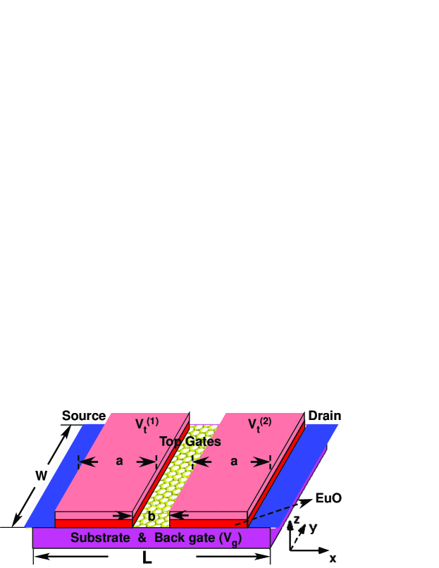
In this work, we propose a bulk graphene based, spin-dependent double-barrier resonant tunneling diode (DB-RTD), which requires only depositing two gated EuO stripsHaugen et al. (2008) on top of a sufficiently wide and short graphene (see upper panel in Fig. 1). In this device, no specific control of the graphene edge type is needed because the transport is dominated by bulk states; no doping’s or defects are required because the ferromagnetism is induced by magnetic insulators; and two ferromagnetic barriers instead of a ferromagnetic superlattice is enough because large energy gaps are induced. We find clear spin-dependent resonant states in the device, which dominate the biased transport when the Fermi energy is setting around the resonant levels. The resonant levels decrease with an increasing bias, resulting in a fewer transversal mode number hence the occurrence of the desired NDR feature. Remarkably, we find a clear significant of a spin selectivity and a region tunability in the spin-dependent NDR: by changing the top gates hence the spin-dependent resonant levels in the device, the spin index of the NDR can be tuned as spin up only, spin down only, or both spins; meanwhile, the central position of the NDR region in each case can be monotonously tuned in a wide bias range. Together with the relative ease in fabrication, these remarkable features make the proposed device an important building block for future spintronic or NDR circuits.
The structure of the paper is as follows. In Sec. II we present the setup of the device and the formula to calculate the stationary envelop function as well as the transmission coefficient for a given spin, energy, incident angle, and bias voltage across the sample. An ab-initio dispersion of graphene on EuOYang et al. (2013); Hallal et al. (2017) and a linear voltage drop through the device are considered. The resulting current-voltage (I-V) characteristics of the device, comprised of a spin-dependent NDR with a spin selectivity and a region tunability, are discussed in the subsequent Sec. III. The mechanism for the arising and tunability of the spin-dependent NDR, as well as possible applications are emphasized. Finally, Sec. IV concludes the paper.
II Setup and Formula
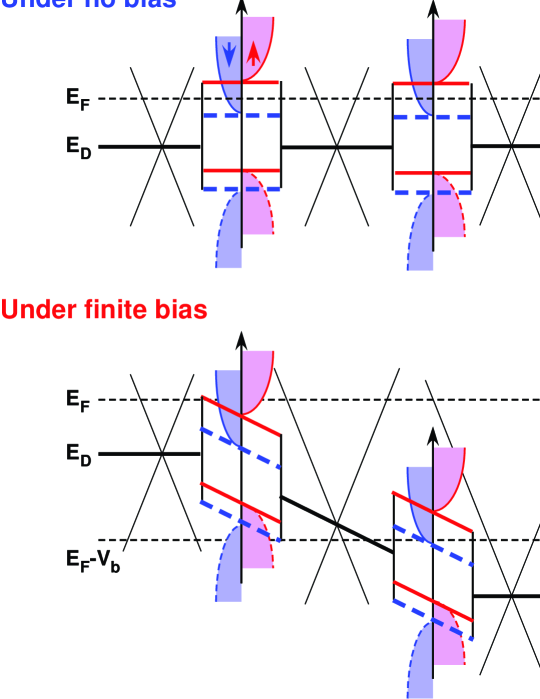
The proposed system is composed of a sufficiently wide (=250 nm) and short rectangular graphene and two rectangular EuO strips on top of it (see the upper panel of Fig. 1). The length of each strip is 21.75 nm and the spacing between them is 8.7 nm. The source and drain electrodes, which may induce a charge doping (), are separated from the EuO strips by two buffer regions of length. The total length is several times smaller than , hence the transport is dominated by bulk statesTworzydło et al. (2006) and no specific control of the graphene edge type is needed. ExperimentsSwartz et al. (2012); Wang et al. (2015); Wei et al. (2016); Zhang et al. (2017) and ab-initio calculationsYang et al. (2013); Hallal et al. (2017) have shown that, through a magnetic proximity effect, the two EuO strips induce ferromagnetism as well as heavy electron doping’s (with a Dirac point of eV) in graphene just underlying them (see the middle panel of Fig. 1). On top of the EuO strips, two top gates () are applied. They are used to tune the local carrier concentrations and to lift up the Dirac points of the two ferromagnetic graphene’s to align with that of the prinstine graphene (see the middle panel of Fig. 1). Therefore, the array of two gated EuO strips creates the desired ferromagnetic double barriers or spin-dependent DB-RTD. Below the substrate, a back gate () is applied to tune the Fermi energy () through the whole sample.
When a bias voltage () is applied between the source and drain, a net current will be produced by the electrons or holes in the source within an energy range of or at zero temperature, see the bottom panel in Fig. 1. Due to the spin difference in the ferromagnetic regions, the current will be spin dependent. Unlike other works which considered a step-like voltage drop through the device, in this work we also consider a linear voltage drop, with , between the source and drain along the -direction.
The magnetic proximity effect in graphene is usually described by a simple Zeeman splitting model,Haugen et al. (2008); Munárriz et al. (2013); Díaz et al. (2014); Lu et al. (2013); Dell’Anna and De Martino (2009); Niu et al. (2008); Faizabadi et al. (2012); Zou et al. (2009) based on which a spin wavevector filtering effect,Lu et al. (2013) a spin conductance filtering effect,Dell’Anna and De Martino (2009) and a tunneling magnetoresistance effect Niu et al. (2008); Faizabadi et al. (2012); Zou et al. (2009) have been proposed. (These effects have also been found in other two-dimensional systems subjected to magnetic modulations; just to cite a few.Wang et al. (2002); Papp et al. (2005); Wu et al. (2011); Shakouri et al. (2015, 2014)) The Zeeman splitting model is roughly estimated from an analogy with a EuO/Al interface and considers only opposite energy shifts for opposite spins added to the linear dispersion of a pristine graphene.Haugen et al. (2008) However, very recent ab-initio calculationsYang et al. (2013); Hallal et al. (2017) and experimentsSwartz et al. (2012); Wang et al. (2015); Wei et al. (2016); Zhang et al. (2017) demonstrate a totally different picture: the gapless and linear Dirac cone for each spin shifts down to a negative Dirac point (), opens a large energy gap (), and changes its Fermi velocity () ( for spin up and spin down), all depending on the spin index; see middle and bottom panels in Fig. 1. For graphene on six bi-layer EuO, the parameters read 42 (-24) meV, 67 (49) meV, and 1.337 (1.628) , respectively.Yang et al. (2013); Song and Dai (2015) OthersZollner et al. (2016); Su et al. (2017); Hallal et al. (2017) and weSong and Dai (2015); Song (2017) have developed effective Hamiltonians in a sublattice-spin direct produce space or a sublattice space, based on which nontrivial effects, such as quantum anomalous Hall effect,Su et al. (2017) simultaneous spin filter and spin valve effect,Song and Dai (2015) electric-field-induced extremely large change in resistance,Song (2017) and pure crossed Andreev reflectionAng et al. (2016) have been explored.
In a sublattice space, the effective Hamiltonian readsBeenakker (2008); Song and Dai (2015); Song (2017)
| (1a) | |||
| Here is a pseudospin Pauli matrices, is a momentum operator, is an index for valley and , and is an identity matrix. For the pristine graphene in the well and the buffer regions, the Hamiltonian is well known | |||
| (1b) | |||
| For the contacted graphene in the source and drain, the Hamiltonian reads | |||
| (1c) | |||
For convenience, below we will express all physical quantities in their dimensionless form, in terms of a characteristic length 56.55nm and a corresponding energy unit 10meV. The transversal momentum ( and are the energy and incident angle of a fermion, respectively) is conserved, and it suffices to solve the longitudinal wave function , where for the contacted, ferromagnetic, and pristine graphene, respectively. However, straightforward decoupling of in Eqs. (1a) and (1b), which contain a linear term of , results in an unsolvable two-order differential equation.Sonin (2009) To solve this problem, we perform a rotation of the Dirac equation by around the -axis in the pseudospin space (see the upper pannel of Fig. 1). The envelope functions become resolvable and the result for the ferromagnetic graphene reads
| (2a) | |||
| where and . Here is the Weber parabolic cylinder function, , and . Note, and [ and ] are spin resolved and have properties of a right (left)-going wave function.Sonin (2009) For the pristine graphene the result becomes | |||
| (2b) | |||
| where and . In the rotated pseudospin space, the envelope functions for the contacted graphene become | |||
| (2c) | |||
where with . In the device source, and , while in the device drain and . and are spin-dependent reflection and transmission coefficients, respectively.

With the standard transfer-matrix method,Born and Wolf (2013) can be obtained by matching the spinor envelope functions in Eqs. (2a), (2b), and (2c) at the potential boundaries. The spin-dependent transmission probability reads for and , and otherwise. The spin-dependent net current at zero temperature can be calculated by the Landauer-Büttiker formalismBüttiker et al. (1985)
| (3) |
where is a current unit with the factor 2 coming from the valley degeneracy. Considering the values of and , , which is one or two orders of magnitudes larger than those in devices based on graphene nanoribbons.Wu et al. (2012); Jiang et al. (2014); Yan et al. (2014); Yang et al. (2015); Xu et al. (2014); Hong et al. (2015); Son et al. (2006); Liu et al. (2016); Munárriz et al. (2013) is an energy integral interval, in which a spin-dependent differential conductance at a given energy can be defined as . It is also seen that, contributes to by a weight of , which is the transversal modes number (TMN) at .Tworzydło et al. (2006)
III Results and Discussion
III.1 Spin-dependent linear conductance at zero bias
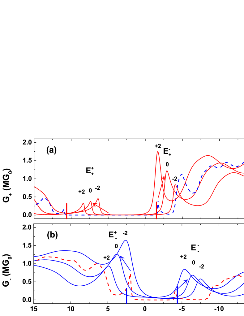
Figure 2 (a,b) show the spin-dependent linear conductance through the unbiased device as a function of the Fermi energy: , where is the quantum conductance. The calculations can be made by following Ref. Song (2017). Here an ideal contacting () is considered. It is seen that, already for a relatively short device ( with and , the dashed curve), its linear conductance for each spin shows a good accordance to the corresponding band gap, whose conduction band minimum (CBM) and valence band maximum (VBM) are indicated by the vertical bars in Fig. 2 (a,b). Inside each energy gap, two resonant peaks and arise, where the subscript stand for spin up and spin down and the superscript stand for the CBM or VBM part. This is a clear significant of resonant tunneling in the device. For a shorter device (1, the solid curves) the resonant peaks shift outside and become stronger (indicated by the arrows). The spin-dependent linear conductance at different top gates are also shown. It is seen that, the resonant levels become larger (smaller) as a positive (negative) top gate is applied. This will play an important role in the gate control of the spin-dependent NDR. Compared with spin up, the resonant tunneling is much weaker for spin down. This is a result of a smaller effective spin Dirac gap, i.e., .Song (2017)
The total conductance is spin dependent, which manifests itself clearly in the polarization, which is defined as and plotted in Fig. 2(c). In Fig. 2(c), near () polarization can be found in the energy ranges between CBMs (VBMs) of different spins. They are much higher than spin polarizations obtained in Refs. Dell’Anna and De Martino (2009); Zou et al. (2009) and can be applied as a highly efficient spin conductance filtering. On the other hand, the spin filtering effect is found to be weaken by the resonant tunneling and can be exactly controlled by the top gates.
III.2 Spin-dependent NDR at finite bias
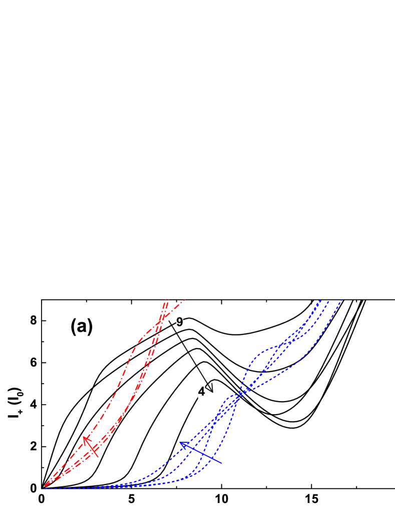
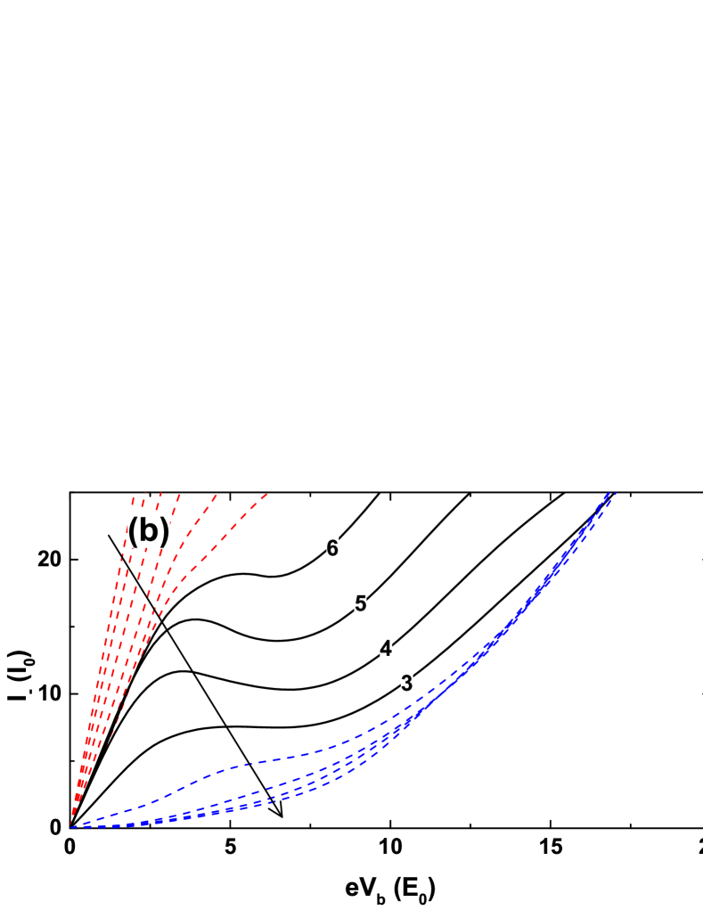
The spin-dependent I-V characteristics of the device with various Fermi energies are plotted in Fig. 3(a,b). It is seen in Fig. 3(a) that, for Fermi energies around the resonant level (black solid), the spin-up current displays obvious NDR. However, for Fermi energies much higher (, red dashed) or smaller (, blue dashed) than the resonant level, the NDR features disappear. The case is the same for spin down as shown in Fig. 3(b), where NDR features are found only for Fermi energies around the resonant level .
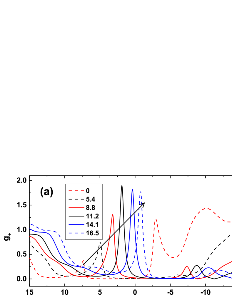
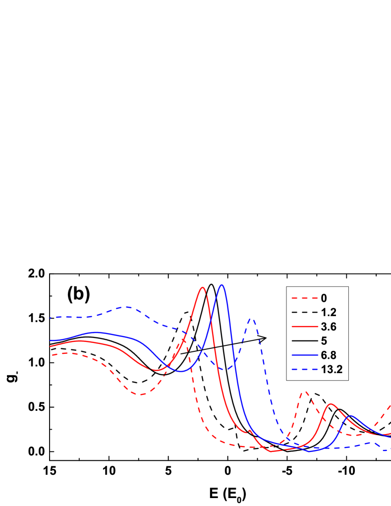
To understand these interesting behaviors, we plot the spin-up differential conductance as a function of energy in Fig. 4(a). Several typical biases in the strongest NDR case () are considered. It is seen that, for Fermi energies around the resonant level, the transport under the considered biases are dominated by the resonant state. As the bias increases from zero (the 0 and 5.4 curves), the resonant peak shifts into the integral interval (the origin of which, , is indicated by the vertical bar) with an increasing peak value. This results in an increase behavior of the spin-up current with an increasing bias in the device. The spin-up current reaches its maximum at a bias of , where the resonant peak has totally inserted into the integral interval. As indicated above, the spin-up resonant state contributes to the spin-up current by a weight of TMN (where ), see Eq. (3). As the bias increases further (the 11.2 curve), the TMN decreases, which results in a decrease behavior of the spin-up current with an increasing bias, i.e., the desired NDR feature. The TMN decreases with the bias because, as the bias increases the positive resonant level is pulled down and gets closer to the Dirac point in the source, i.e., becomes smaller as becomes smaller. The spin-up current achieves its minimum at a larger bias (the curve), where the pull-down resonant level almost aligns to the Dirac point in the source and the TMN approaches near zero. However, as the bias increases further (the 16.5 curve), the pulling down of a negative resonant level leads to an increase of the TMN, i.e., becomes bigger as becomes smaller. As a result, the spin-up current increases again.
On the other hand, for Fermi energies far from the spin-up resonant level, the biased transport is also contributed by a quasi-ballistic state outside the spin Dirac gap, see Fig. 4(a). As a result, the bias-induced decrease of the TMN (integral weight) is counteracted by the bias-induced increase of the integral interval, and the NDR feature disappears. For spin down, the NDR is much less pronounced. This stems from a more expanding resonant peak, which is shown in Fig. 4(b), where several typical biases for the strongest NDR case () are considered.
III.3 Top-gate control of the spin-dependent NDR
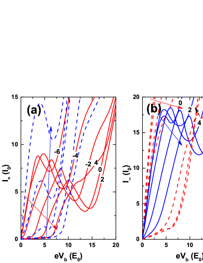
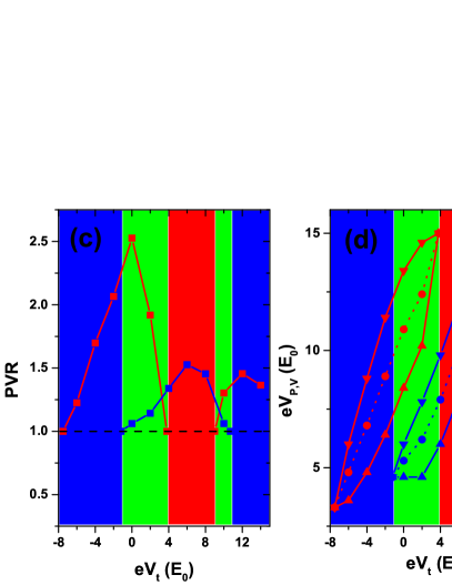
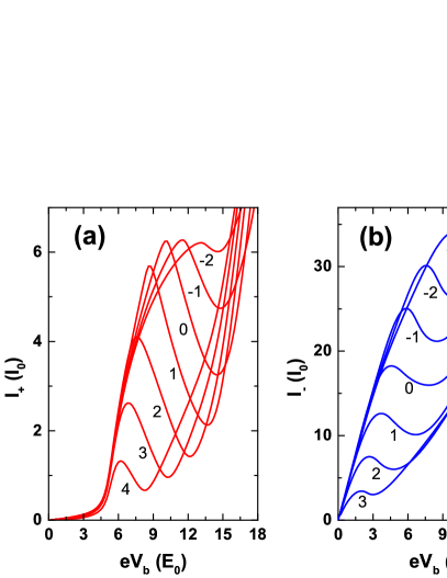
The spin-dependent I-V characteristics at various top gates are shown in Fig. 5(a,b). Here is focused, for which both spins display obvious NDRs. It is seen that, as the top gates increase in the considered range, spin up displays NDR (the -6 to 2 curves), no NDR (the 4 to 8 curves), and NDR (the 10 to 14 curves), respectively. In contrast, spin down shows no NDR (the -6 to -2 curves), NDR (the 0 to 10 curves), and no NDR (the 12 to 14 curves), respectively. This is according to that the resonant levels , , and are sequentially lifted up around the Fermi energy and dominate the biased transport. For each spin, the peak-to-valley currents ratio (PVR) are summarized in Fig. 5 (c) as a function of the top gates. It is seen that, according to the occurrence of the spin-dependent NDR only at certain top gates, the PVR shows a non-monotonous dependence on the top gates, increasing from 1 (no NDR) to certain value and then decreasing to 1 again. The maximal PVR for each spin is found at certain top gates that the lifted resonant level is slightly lower than the Fermi energy. For spin up, the value reads 2.5, which is comparable with those obtained in experiments on spin-independent NDRs.Britnell et al. (2013); Sharma et al. (2015)
Although the NDR happens at different top gates for spin up and spin down, NDRs for both spins can be achieved for certain top gates, see the green windows in Fig. 5 (c) and the curves in Fig. 5(a,b). In Fig. 5 (a,b), it is also observed that the NDR regions for different spins do not overlap. As a result, the proposed device can be applied as a dual-spin Esaki diode: at low biases spin down displays NDR and at high biases spin up displays NDR. The dual-spin NDR occurs because the resonant levels are lifted up that the Fermi energy lies between and ( and ). For top gates higher (lower) than the left green window in Fig. 5(c), i.e., the red (blue) windows, only spin down (spin up) shows NDR while the current for the other spin increases monotonously with the bias. This can be applied as a single-spin Esaki diode. Hence, as the top gates increases from -7 to 15, the proposed device works consecutively as a spin-up only, dual-spin, spin-down only, dual-spin, and spin-up only Esaki diode. In other words, spin-dependent NDR with spin selectivity can be realized in the proposed device, by simply changing the top gates.
The NDR regions () for each spin are summarized in Fig. 5 (d) as a function of the top gates. It is seen that, when the top gates increase from -7.5 to -1.2 (the left blue window in Fig. 5 (d)), the center of the spin-up NDR region shifts monotonously from 3.3 to 9.7. This implies that, the operation region of the spin-up Esaki diode is variable in a large range of 64meV. When increase from -1.2 to 3.7 (the left green window in Fig. 5 (d)), both the spin-up and spin-down NDR regions of the dual-spin Esaki diode are tunable. The variable ranges are meV and meV, respectively. For top gates changed between 3.8 and 9 (the red window in Fig. 5 (d)), the operation region of the spin-down Esaki diode is monotonously tunable in a range of 45 meV.
The spin selectivity and region tunability of the spin-dependent NDR can be understood as follows. As the top gates increase, the spin-dependent resonant levels formed between the ferromagnetic double barriers are lift. As a result, , , and are consecutively closed to the fixed Fermi energy hence dominate the biased transport, solely or simultaneously. The former leads to a single-spin Esaki diode while the latter results in a dual-spin Esaki diode. On the other hand, for each resonant level dominating the biased transport, its deviation from the Dirac point in the source enlarges with the increasing top gates, see Fig. 2(a,b). From the NDR mechanism discussed in Sec. III.2, the decrease of the TMN (integral weight) hence the spin-dependent NDR should be happen at a higher bias. In Fig. 3 the spin-dependent NDR region is also found to be controlled by the Fermi energy. However, the change is non monotonous.
Spin oscillator, spin amplifier, spin switching, and spin memory can be realized based on a spin-dependent NDR. The gate-induced spin selectivity in the proposed device adds a spin degree of freedom to these spin devices: by simply changing the top gates as low, high, and medium values, spin devices for spin up only, spin down only, or both spins (occurring sequentially) can be respectively realized. On the other hand, the gate-induced region tunability in the proposed device further adds an output degree of freedom to these spin devices. This may be especially important in spin switchinges and spin memories, whose lowest output voltage and two stored states are found to be exactly determined by the position of the NDR regions (see Ref. Mizuta and Tanoue (2006) and relevant references therein).
III.4 Electrode doping effect
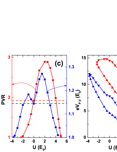
We at last investigate the electrode doping effect on the spin-dependent NDR. Fig. 6(a,b) show the spin-dependent I-V characteristics at various light contact doping’s. The spin-dependent PVR and NDR region () are summarized in Fig. 6(c,d) as a function of the contact doping. A dual-spin NDR ( and ) is considered. As can be seen, the dual-spin NDR only maintains for -23meV44meV. For smaller than -23meV or larger than 44meV, the NDR becomes spin-down only or spin-up only. The single-spin NDR feature even disappears for smaller than -37meV or larger than 50meV. However, for familiar metal electrodes such as Ag, Ti, Cu, Au, and Pt at their equilibrium distances to graphene, the contact doping’s are -320meV, -230meV, -170meV, 250meV, and 320meV, respectively.Lee et al. (2008); Giovannetti et al. (2008) These values are much larger than the doping range (meV44meV) the dual-spin NDR can survive. To maintain the proposed NDR, one possible way is to tune the metal-graphene distances to special values (e.g., Au/Cu/Ag at 3.2/3.4/3.7 ) to obtain ideal doping’s.Giovannetti et al. (2008) Another possible way is to adopt improved contacts such as Ti/Au. Lee et al. (2008); Robinson et al. (2011)
In Fig. 6(a,b) it is also clear that, both the peak and valley currents decrease with an increasing doping. This is a result of that, the TMNs for the dominating resonant states () decrease with the doping . However, the peak and valley currents decrease differently. As shown in Fig. 4, the peak current is dominated by the resonant peak away from the Dirac point, so as the Dirac point is lifted up it decreases first gently and then sharply, see Fig. 6(a); in contrast, the valley current is dominated by the resonant peak around the Dirac point, so as the Dirac point is lifted up it decreases first sharply and then gently. As a result of this contrast, the PVR first increases and then decreases with an increasing doping, see Fig. 6(c). (The spin-down PVR shows an exception for -10meV0meV because the resonant peak for the peak current extends considerably to the Dirac point.) Importantly, the PVR for the spin-up NDR increases from 1.92 at an ideal doping to 2.89 at a light hole doping of 22meV, with a large enhancement factor of 51. For spin down, the PVR of 1.15 at an ideal contacting approaches its maximum of 1.27 at a light hole doping of 15meV, with an enhancement factor of 10. The above specific metal-graphene distances can be enlarged a little to achieve these light hole doping’sGiovannetti et al. (2008) and larger PVR’s.
In Fig. 6(d) it is seen that, the NDR regions are rather sensitive to the contact doping’s, with variable ranges of 84 meV and 110 meV for spin up and spin down, respectively. The larger the contact doping, the lower the NDR regions. This is because as increases, the Dirac node in the source gets closer to the resonant levels and the biases needed to align them become smaller. However, using the contact doping instead of the top gates to tune the NDR regions would be much harder.
IV Conclusion
In summary, we have proposed a bulk graphene based, spin-dependent NDR device, which is composed of a sufficiently wide and short graphene and two gated EuO strips deposited on top of it. An ideal or light hole electrode doping is also essential. The spin-dependent NDR arises because the energies (transversal mode numbers) of the spin-dependent resonant states decrease with an increasing bias. Compared with spin-dependent NDR devices based on zigzag or armchair GNRs, the proposed device holds the advantages of no need of edge tailors, generation of larger currents, and most importantly, features of a spin selectivity and a region tunability. These remarkable features stem from a top-gate control of the deviations of the spin-dependent resonant levels from the Fermi energy and the Dirac point in the source electrode, respectively. They add a spin and a bias degree of freedom to conventional NDR-based devices, which paves a way for design of a whole new class of NDR circuits such as spin-selectable and output-tunable spin switching and spin memory.
Acknowledgements
This work was supported by the National Natural Science Foundation of China (NSFC) under Grant No. 11404300 and the ST Innovation Fund of IEE, CAEP under Grant No. S20140807.
References
- Alekseev and Pavlidis (2000) E. Alekseev and D. Pavlidis, Solid State Electron 44, 941 (2000).
- Laskar et al. (1989) J. Laskar, A. Ketterson, J. Baillargeon, T. Brock, I. Adesida, K. Cheng, and J. Kolodzey, IEEE Electron Device Lett. 10, 528 (1989).
- Liu et al. (1997) W.-C. Liu, J.-H. Tsai, W.-S. Lour, L.-W. Laih, S.-Y. Cheng, K.-B. Thei, and C.-Z. Wu, IEEE Trans. Electron Devices 44, 520 (1997).
- Van Der Wagt (1999) J. Van Der Wagt, Proc. IEEE 87, 571 (1999).
- Wu et al. (2012) T.-T. Wu, X.-F. Wang, M.-X. Zhai, H. Liu, L. Zhou, and Y.-J. Jiang, Appl. Phys. Lett. 100, 052112 (2012).
- Jiang et al. (2014) C. Jiang, X.-F. Wang, and M.-X. Zhai, Carbon 68, 406 (2014).
- Yan et al. (2014) S.-L. Yan, M.-Q. Long, X.-J. Zhang, and H. Xu, Phys. Lett. A 378, 960 (2014).
- Yang et al. (2015) X.-F. Yang, W.-Q. Zhou, X.-K. Hong, Y.-S. Liu, X.-F. Wang, and J.-F. Feng, J. Chem. Phys. 142, 024706 (2015).
- Xu et al. (2014) T. Xu, J. Huang, and Q.-x. Li, Chinese J. Chem. Phys. 27, 653 (2014).
- Li et al. (2017) X. F. Li, L. Liu, Q. Yan, Q. K. Li, Y. Wang, M. Deng, and Q. Qiu, Phys. Chem. Chem. Phys. 19, 2674 (2017).
- Hong et al. (2015) X. Hong, Y. Kuang, C. Qian, Y. Tao, H. Yu, D. Zhang, Y.-S. Liu, J. Feng, X. Yang, and X.-F. Wang, J. Phys. Chem. C. 120, 668 (2015).
- Son et al. (2006) Y. Son, M. Cohen, and S. Louie, Nature 444, 347 (2006).
- Liu et al. (2016) N. Liu, J. Liu, K. Yao, Y. Ni, and S. Wang, J. Appl. Phys. 119, 104301 (2016).
- Munárriz et al. (2013) J. Munárriz, C. Gaul, A. V. Malyshev, P. Orellana, C. A. Müller, and F. Domínguez-Adame, Phys. Rev. B 88, 155423 (2013).
- Díaz et al. (2014) E. Díaz, K. Miralles, F. Domínguez-Adame, and C. Gaul, Appl. Phys. Lett. 105, 103109 (2014).
- Bai et al. (2010) J. Bai, R. Cheng, F. Xiu, L. Liao, M. Wang, A. Shailos, K. L. Wang, Y. Huang, and X. Duan, Nature Nanotech. 5, 655 (2010).
- Llinas et al. (2017) J. P. Llinas, A. Fairbrother, G. B. Barin, W. Shi, K. Lee, S. Wu, B. Y. Choi, R. Braganza, J. Lear, N. Kau, W. Choi, C. Chen, Z. Pedramrazi, T. Dumslaff, A. Narita, X. Feng, K. Müllen, F. Fischer, A. Zettl, P. Ruffieux, E. Yablonovitch, M. Crommie, R. Fasel, and J. Bokor, Nat. Commun. 8, 633 (2017).
- Chhowalla et al. (2016) M. Chhowalla, D. Jena, and H. Zhang, Nat. Rev. Mater. 1, 16052 (2016).
- Haugen et al. (2008) H. Haugen, D. Huertas-Hernando, and A. Brataas, Phys. Rev. B 77, 115406 (2008).
- Yang et al. (2013) H.-X. Yang, A. Hallal, D. Terrade, X. Waintal, S. Roche, and M. Chshiev, Phys. Rev. Lett. 110, 046603 (2013).
- Hallal et al. (2017) A. Hallal, F. Ibrahim, H. Yang, S. Roche, and M. Chshiev, 2D Mater. 4, 025074 (2017).
- Tworzydło et al. (2006) J. Tworzydło, B. Trauzettel, M. Titov, A. Rycerz, and C. W. Beenakker, Phys. Rev. Lett. 96, 246802 (2006).
- Swartz et al. (2012) A. G. Swartz, P. M. Odenthal, Y. Hao, R. S. Ruoff, and R. K. Kawakami, ACS Nano 6, 10063 (2012).
- Wang et al. (2015) Z. Wang, C. Tang, R. Sachs, Y. Barlas, and J. Shi, Phys. Rev. Lett. 114, 016603 (2015).
- Wei et al. (2016) P. Wei, S. Lee, F. Lemaitre, L. Pinel, D. Cutaia, W. Cha, F. Katmis, Y. Zhu, D. Heiman, J. Hone, et al., Nature Mater. 15, 711 (2016).
- Zhang et al. (2017) Y. Zhang, X. Sui, D. Ma, W. Duan, and L. He, arXiv preprint arXiv:1704.05965 (2017).
- Lu et al. (2013) W.-T. Lu, W. Li, Y.-L. Wang, H. Jiang, and C.-T. Xu, Appl. Phys. Lett. 103, 062108 (2013).
- Dell’Anna and De Martino (2009) L. Dell’Anna and A. De Martino, Phys. Rev. B 80, 155416 (2009).
- Niu et al. (2008) Z. Niu, F. Li, B. Wang, L. Sheng, and D. Xing, Eur. Phys. J. B. 66, 245 (2008).
- Faizabadi et al. (2012) E. Faizabadi, M. Esmaeilzadeh, and F. Sattari, Eur. Phys. J. B. 85, 1 (2012).
- Zou et al. (2009) J. Zou, G. Jin, and Y.-q. Ma, J. Phys. Condens. Matter 21, 126001 (2009).
- Wang et al. (2002) X. Wang, P. Vasilopoulos, and F. Peeters, Phys. Rev. B 65, 165217 (2002).
- Papp et al. (2005) G. Papp, P. Vasilopoulos, and F. Peeters, Phys. Rev. B 72, 115315 (2005).
- Wu et al. (2011) Z. Wu, F. Peeters, and K. Chang, Appl. Phys. Lett. 98, 162101 (2011).
- Shakouri et al. (2015) K. Shakouri, H. Simchi, M. Esmaeilzadeh, H. Mazidabadi, and F. Peeters, Phys. Rev. B 92, 035413 (2015).
- Shakouri et al. (2014) K. Shakouri, P. Vasilopoulos, V. Vargiamidis, and F. Peeters, Phys. Rev. B 90, 125444 (2014).
- Song and Dai (2015) Y. Song and G. Dai, Appl. Phys. Lett. 106, 223104 (2015).
- Zollner et al. (2016) K. Zollner, M. Gmitra, T. Frank, and J. Fabian, Phys. Rev. B 94, 155441 (2016).
- Su et al. (2017) S. Su, Y. Barlas, J. Li, J. Shi, and R. K. Lake, Phys. Rev. B 95, 075418 (2017).
- Song (2017) Y. Song, J. Phy. D: Appl. Phys. (2017).
- Ang et al. (2016) Y. S. Ang, L. Ang, C. Zhang, and Z. Ma, Phys. Rev. B 93, 041422 (2016).
- Beenakker (2008) C. Beenakker, Rev. Mod. Phys. 80, 1337 (2008).
- Sonin (2009) E. Sonin, Phys. Rev. B 79, 195438 (2009).
- Born and Wolf (2013) M. Born and E. Wolf, Principles of optics: electromagnetic theory of propagation, interference and diffraction of light (Elsevier, 2013).
- Büttiker et al. (1985) M. Büttiker, Y. Imry, R. Landauer, and S. Pinhas, Phys. Rev. B 31, 6207 (1985).
- Britnell et al. (2013) L. Britnell, R. Gorbachev, A. Geim, L. Ponomarenko, A. Mishchenko, M. Greenaway, T. Fromhold, K. Novoselov, and L. Eaves, Nat. Commun. 4, 1794 (2013).
- Sharma et al. (2015) P. Sharma, L. S. Bernard, A. Bazigos, A. Magrez, and A. M. Ionescu, ACS Nano 9, 620 (2015).
- Mizuta and Tanoue (2006) H. Mizuta and T. Tanoue, The physics and applications of resonant tunnelling diodes, Vol. 2 (Cambridge University Press, 2006).
- Lee et al. (2008) E. J. Lee, K. Balasubramanian, R. T. Weitz, M. Burghard, and K. Kern, Nature Nanotech. 3, 486 (2008).
- Giovannetti et al. (2008) G. Giovannetti, P. Khomyakov, G. Brocks, V. v. Karpan, J. Van den Brink, and P. J. Kelly, Phys. Rev. Lett. 101, 026803 (2008).
- Robinson et al. (2011) J. A. Robinson, M. LaBella, M. Zhu, M. Hollander, R. Kasarda, Z. Hughes, K. Trumbull, R. Cavalero, and D. Snyder, Appl. Phys. Lett. 98, 053103 (2011).