Vertically-Illuminated, Resonant-Cavity-Enhanced, Graphene-Silicon Schottky Photodetectors
Abstract
We report vertically-illuminated, resonant cavity enhanced, graphene-Si Schottky photodetectors (PDs) operating at 1550nm. These exploit internal photoemission at the graphene-Si interface. To obtain spectral selectivity and enhance responsivity, the PDs are integrated with an optical cavity, resulting in multiple reflections at resonance, and enhanced absorption in graphene. Our devices have wavelength-dependent photoresponse with external (internal) responsivity20mA/W (0.25A/W). The spectral-selectivity may be further tuned by varying the cavity resonant wavelength. Our devices pave the way for developing high responsivity hybrid graphene-Si free-space illuminated PDs for free-space optical communications, coherence optical tomography and light-radars.
I Introduction
Near infrared (NIR) photodetection at 1550nm is of paramount importance for a variety of applications, ranging from optical communicationsAgra2010 ; LeitJOFCR2005 ; KausIEEE2016 ; Ijaz2012 to remote sensingFlooPERS2001 ; ParriAGU2011 . In modern telecom systems, operation at 1550nm benefits from a reduced light absorption in optical fibersAgra2010 . In free-space optical communications (FSO)LeitJOFCR2005 ; KausIEEE2016 ; Ijaz2012 and light-radars (LIDARs)FlooPERS2001 ; ParriAGU2011 , this minimizes the propagation losses in fogKausIEEE2016 and humid conditionsIjaz2012 , due to lower optical absorption and scattering compared to wavelengthsm, and improves eye safety because the outer layer of the eye (cornea) absorbs light at 1550nm and does not allow it to focus on the retinaFlooPERS2001 ; KausIEEE2016 . In optical coherence tomography (OCT), a non-invasive imaging technique for biological tissuesIshiBOE2012 , the advantages of using 1550nm are enhanced penetration depth, due to lower scattering in tissue with respect to shorter wavelengthsIshiBOE2012 , and enhanced imaging contrast at deeper penetration depths, where multi-scattering processes dominateIshiBOE2012 .
Many photodetectors (PDs) for 1550nm have been proposedAgra2010 ; Sze2006 ; EngN2015 ; CasalJOA2012 . For telecom and datacom applications, these typically rely on a waveguide configurationKangNP2009 ; MasiAPL2002 ; KoesIEEE2006 ; MichNP2010 ; AsseN2010 ; ZhuAPL2008 ; GoykNL2011 ; GoykOE2012 ; CasaJAP2013 ; AkbaOE2010 , in which optical confinement and guiding contribute to enhanced light absorption and photodetection. On the other hand, for FSO, OCT and LIDARs, NIR PDs for free-space illumination are requiredLeitJOFCR2005 ; KausIEEE2016 ; Ijaz2012 ; FlooPERS2001 ; ParriAGU2011 ; IshiBOE2012 . At present, III-V compound (e.g. InGaAs, InP)WaldIEEE1996 ; KangIEEE2002 and group IV (Ge)KangNP2009 ; MasiAPL2002 ; KoesIEEE2006 ; MichNP2010 semiconductors are the materials of choice for vertically-illuminated NIR PDs, due to their high (90%)Sze2006 NIR absorption. The ever growing demand and performance requirements in modern systems (such as bit-rate, number of pixels, imaging matrix size, operation and processing speed)Agra2010 ; Sze2006 make it crucial to integrate PDs with supporting circuitry (drivers, amplifiers, processors) on the same chip. Since modern microelectronics relies on mature complementary metal-oxide-semiconductor (CMOS) technology, the development of NIR PDs on Si is promising for integrated microsystems, combining both optical and electronic functionalities. III-V materials are not compatible with standard CMOS fabrication processes because of cross-contamination and dopant redistribution effectsSzeVLSI2003 , and are typically manufactured in separate facilitiesSzeVLSI2003 . They can be later bonded with CMOS chips using advanced packaging and assemblingLau1999 . However, the overall performance can degrade due to packaging parasitics (e.g. parasitic capacitance and inductance) and cross-talks associated with the wire-bond leadsLau1999 . Epitaxially grown Ge on Si provides a competitive platform to InGaAs and InP based NIR photodetectionKoesIEEE2006 ; HaraASS2004 ; WangS2011 . Nevertheless, due to defectsSzeVLSI2003 and dislocations-like recombination centers at the Si-Ge interfaceKoesIEEE2006 ; HaraASS2004 ; WangS2011 , these PDs typically show larger leakage currentWangS2011 and smaller shunt resistanceWangS2011 compared to III-V devices, resulting in increased noise (thermal and shot)KoesIEEE2006 . To reduce the defects density, a two-step Ge deposition is commonly usedKoesIEEE2006 ; HaraASS2004 ; WangS2011 , however it involves high (650∘C) temperature processesWangS2011 that can sacrifice the thermal budget, which limits the amount of thermal energy available to the wafer during the fabrication process.
An alternative and promising approach for monolithic integration of NIR PDs with CMOS electronics is to perform sub-bandgap photodetection in Si exploiting the internal photoemission process (IPE) in a Schottky junctionSze2006 ; PetePIEEE1962 ; BronNN2015 ; CasalJQE2016 . In this case, photoexcited carriers from the metal electrode can be emitted to Si over the Schottky barrier , allowing NIR detection for photon energy hSze2006 ; PetePIEEE1962 ; BronNN2015 . Schottky PDs have been successfully used in IR focal plane arrays (FPA)KimaOR1998 , monolithically integrated with CMOS readout electronics and charge coupled devices (CCDs)Sze2006 . The advantages of the Schottky junction configuration over other PD types (pn and pin junctions, quantum wells) stem from its simple structureSze2006 , easy fabrication and integration with CMOS technologySze2006 . The main drawback is the limited ()GoykA2014 ; CasaS2016 internal quantum efficiency (IQE) of the IPE process, defined as the number of carriers emitted to Si per absorbed photon. This is mainly because the momentum mismatch between the electron states in the metal and Si results in a specular reflection of excited electrons at the Schottky interfaceSze2006 ; GoykA2014 . The IQE is linked to the PD internal (external) responsivity Rint (Rext), defined as the ratio between the photocurrent Iph and the absorbed (incident) optical power , i.e = = and ==Sze2006 , where q is the electron charge and A is the absorptance. As a result, limited IQE leads to limited responsivity, so that the highest Rext reported so far in vertically-illuminated Si Schottky PDs operating at 1550nm is5mA/WDesiO2015 , much lower than the 0.5-0.9A/W for III-VSze2006 and GeSze2006 based PDs. Graphene/Si Schottky PDs at 1550nm have been demonstrated both in free-spaceAmirIEEE2013 and guided mode configurationsWangNP2013 ; GoykNL2016 , with up to 10mA/W and 0.37A/W respectively. In these devices, a single layer graphene (SLG) acts as electrode in contact with Si, forming a Schottky junction with rectifying characteristicsChenNL2011 ; AnNL2013 ; BartoPR2016 . In general, graphene is an attractive material for photonics and optoelectronicsFerrN2015 ; KoppNN2014 ; BonaNP2010 ; SunACS2010 . Its integration with Si may allow the development of miniaturized and cost-effective hybrid optical devices and functionalitiesSorianCM2017 . In the case of SLG/Si Schottky PDs, SLG integration allows absorption of NIR photons with energy below the Si bandgap in close proximity to the Schottky interfaceAmirIEEE2013 ; AnNL2013 ; WangNP2013 ; GoykNL2016 , leading to increased IPE IQE. However, the SLG absorption in NIR is2.3NairS2008 ; DawlAPL2008 , and the vast majority of optical power does not contribute to photodetection. As a result, vertically-illuminated SLG/Si Schottky PDs have a limited R10mA/WAmirIEEE2013 at 1550nm, over one order of magnitude lower compared to R0.37A/WGoykNL2016 for the waveguide-integrated configuration, in which light is fully absorbed in SLG upon optical guiding.
Here we increase Rext of free-space illuminated graphene/Si Schottky PDs by combining a Schottky junction with an optical Fabry-Perot (F-P) cavity to enhance light interaction and absorption at the SLG/Si interface. We show that the PD spectral response and responsivity peaks coincide with F-P resonances, with Rext increasing with the number of light round trips inside the cavity. Taking advantage of multiple (5) light reflections at resonance, we obtain spectrally-selective photoresponse with maximum Rext (Rint)20mA/W (0.25A/W), the highest reported so far for vertically-illuminated Si PDs at 1550nm. Our device paves the way for high responsivity hybrid graphene/Si PDs for NIR.
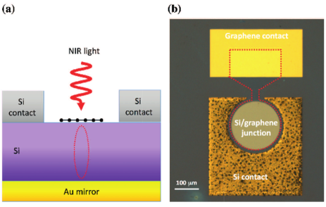
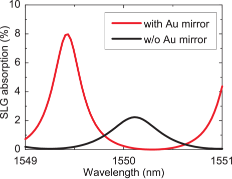
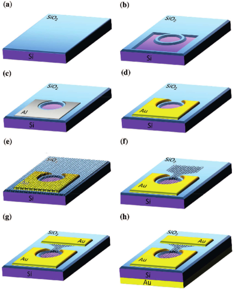
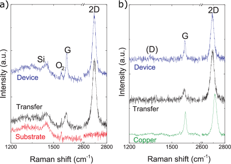
Fig.1 illustrates our F-P cavity integrated SLG/Si Schottky PD. The resonant structure consists of a Si slab layer confined between SLG/Si top and Au bottom mirrors. When vertically-illuminated at resonance, light circulates inside the cavity leading to increased absorption at the SLG/Si interface, resulting in enhanced IPE from SLG to Si. Fig.2 shows a simulation of SLG absorption in the integrated F-P cavity PD. For this we use the transfer matrix methodMuriIEEE1997 and a cavity length L=200m. The Au permittivity =-115+11.3i (at 1550nm) is assumed to follow the Drude model including dampingJCPRB1972 . The permitivity of SLG =1.8+16.4i (at 1550nm) is calculated from its optical conductivity , i.e. , where is the angular frequency, is the permitivity of vacuum, and =0.35nm is the SLG thickness. =61-4.3i [S] includes both contributions from the inter- and intraband transitionsFalk&Pers2007 ; Falk&Varl2007 , assuming a SLG doping0.25eV and scattering time50fs. The simulation indicates that the absorption peaks are spaced by 1.65nm (Fig.2), matching the free-spectral range (FSR) of the F-P cavityAgra2010 : FSR=, where is the illumination wavelength, is the group index of Si around 1550nm, estimated to be 3.61LiJPC1993 , n=3.45 is the refractive index of Si at 1550nmLiJPC1993 , and is the dispersion. We get peak absorptances2.2 and 8.5 for finesse (i.e ratio between FSR and resonance linewidth) of 3 and 5.3 without and with Au mirror, respectively (Fig.2). The peak absorptance for the larger finesse (Au mirror) is4 times higher that for the lower finesse (Si/air mirror), due to larger number of light round trips and optical energy build-up inside the F-P cavity.
The device fabrication process is presented in Fig.3. We use a double-polished, low-doped (1015cm-3), 200m thick Si substrate to minimize the scattering and free-carriers losses in the F-P cavity. First, a 100nm thick SiO2 layer is deposited by e-beam evaporation, Fig.3a, then patterned by optical lithography using a laser-writer (Microtech), followed by wet etching of SiO2 in a buffer-oxide-etch (BOE) solution, Fig.3b. Next, Al ohmic contacts to the p-type Si are realized by an additional lithographic step, followed by lift-off and alloying at 460∘C for 30min in a forming gas (5.7 H2 in N2), Fig.3c. To protect the Al pads from subsequent treatments involving HF, we cover Al with an Au layer using optical lithography, Cr/Au (3nm/50nm) evaporation and lift-off, Fig.3d. The ohmic contact imperfections (black spots) in Fig.1b arise from the Al/Si alloy process.
SLG is grown by chemical vapor deposition (CVD) on a 35-m-thick Cu foil, following the process described in Ref.52. The quality of the material is monitored by Raman spectroscopy using a Renishaw InVia system equipped with a 100 objective at 514.5nm and a laser power below 300W. Fig.4b (green curve) shows the spectrum of SLG on Cu, after the removal of the background Cu photoluminescence (PL)LagatAPL2013 . The two most intense features are the G and the 2D peak, with no significant D peak. The 2D peak is single-Lorentzian, signature of SLGFerrPRL2006 . The position of the G peak, Pos(G), is1595cm-1, with FWHM(G)9.5cm-1. The 2D peak position, Pos(2D) is2712cm-1 with FWHM(2D)29cm-1. The 2D to G peak intensity and area ratios, I(2D)/I(G) and A(2D)/A(G), are1.9 and 5.8, respectively, suggesting a p-doping400meVFerrNN2013 ; DasNN2008 ; BrunACS2014 . After growth, the SLG is wet-transferred to the target substrate, Fig.3e. The film is coated with 500nm polymethyl methacrylate (PMMA), followed by Cu etching in ammonium persulfate (APS). The resulting SLG/PMMA film is rinsed in water to remove APS residuals. To obtain a SLG/Si Schottky interface without a native oxide layer, we transfer SLG in diluted HF in deionized (DI) water (HF/DI water; 1:100)GoykNL2016 . After removing the APS residuals, the SLG/PMMA layer is placed in a plastic beaker containing 5mL/500 mL HF and DI water. Next, the target substrate is first dipped in a buffered oxide etch (BOE) for 5s to etch the native Si oxide and then used to lift the floating SLG/PMMA layer. As a result, during drying, HF at the SLG/Si interface prevents Si oxidation(GoykNL2016, ). After drying, the sample is placed in acetone to dissolve the PMMA, leaving the SLG covering the target substrate, Fig.3e. After transfer, we use additional optical lithography steps to shape the SLG by oxygen plasma and then deposit Cr/Au (3nm/50nm) contacts by evaporation, followed by lift-off, Fig.2f. Before evaporation, a mild (0.5W, 20s) Ar plasma (Moorfield NanoETCH) is applied on the exposed SLG areas for PMMA residuals cleaning leading to low (100) contact resistance at the metal-SLG interface that was separately estimated using a transfer length method . Finally, a bottom mirror is realized by 100nm-thick-Au layer, thermally evaporated on the backside, Fig.3h. Fig.1b shows an optical image of a representative device, where the SLG boundaries are highlighted by a red dashed line. The SLG quality after transfer and after the complete fabrication process is also monitored by Raman spectroscopy. The Raman spectrum of SLG after transfer is shown in Fig.3b, black curve. This is obtained by point-to-point subtraction of the reference Si spectrum (Fig.4a, red curve) from the transferred SLG (Fig.4a, black curve), when the intensities in both spectra are normalized to the third order Si peak at 1450cm-1 (TempPRB1973, ). The 2D peak after transfer is a single-Lorentzian, Pos(2D)2691cm-1 with FWHM(2D)35cm-1. Pos(G) is 1587.5cm-1 with FWHM(G)19.6cm-1. The 2D to G peak intensity and area ratios, I(2D)/I(G) and A(2D)/A(G), are 4.32 and 7.16 respectively, suggesting a p-doping2.41012 cm-2 (200meV)FerrNN2013 ; DasNN2008 ; BaskPRB2009 . Fig.4a (blue curve) plots the SLG Raman spectrum after device fabrication and point-to-point subtraction of the Si reference using the same procedure. After device fabrication Pos(G)=1592.4cm-1, FWHM(G)10.7cm-1, Pos(2D)2691.4cm-1 FWHM(2D)31.1cm-1. I(2D)/I(G) and A(2D)/A(G) are 2.53 and 6.3 respectively, indicating doping91012cm-2 (290meV)FerrNN2013 ; DasNN2008 ; BaskPRB2009 . We also get I(D)/I(G)0.14, indicating that the fabrication process does introduce significant defects in the SLG electrode(CancNL2011, ; BrunACS2014, ).
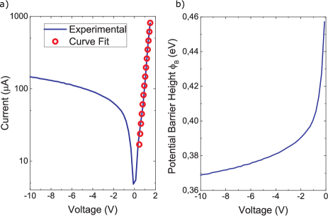
To electrically characterize the PD, we measure the current-voltage (I-V) characteristics of the SLG/Si Schottky junction, Fig.5a. The device shows rectifying I-V diode behavior, which follows the Schottky diode equationSze2006 ; TongPRX2012 :
| (1) |
where , is the Schottky barrier height (SBH) at zero voltage, is the SBH change due to applied voltage bias, A∗ is the Richardson constant (32 A/cm2K2 for p-type SiSze2006 ), A is the junction area, kBT is 26meV at room temperature, is the diode ideality factor, defined as the deviation of the measured I-V curve from the ideal exponential behaviorSze2006 , and Va is the applied voltage. is typically dominant in reverse bias because of the higher potential drop on the Schottky junction, resulting in a more pronounced barrier-lowering Schottky effectSze2006 ; TongPRX2012 and SLG Fermi level shiftAnNL2013 ; TongPRX2012 ; BartoPR2016 . On the other hand, in forward bias the potential drop is limited by the built-in voltage (V1V)Sze2006 , so that can be neglected and . We estimate SBH in forward bias by fitting the experimental data with Eq.1 and using and as fitting parameters. We get 0.46eV and 11. These are in the range of previously reported values (0.410.47 and 230) for SLG/Si Schottky diodesAmirIEEE2013 ; AnNL2013 ; WangNP2013 ; GoykNL2016 ; BartoPR2016 ; ChenNL2011 . By fitting the I-V curve in reverse bias we get the SBH dependence on applied reverse voltage and find up to80meV at -10V, Fig.5b.
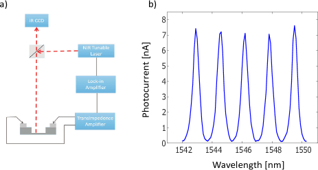
The opto-electronic characterizations is carried out using the set-up of Fig.6a. The signal from a tunable laser (ANDO AQ4321D) is collimated, chopped and split between the reference, used for continuous power monitoring, and the device under test. The PD illumination is inspected by an IR camera. The photocurrent is amplified with a transimpedance amplifier (CVI Melles Griot 13AMP005) and fed to a lock-in amplifier (Signal Recovery 7280 SDP) for measuring the photoresponse. The incident optical power Pinc is measured separately with a InGaAs PD (Thorlabs DET410). Fig.6b plots the spectral response under reverse voltage VR=1V. The device demonstrates spectral selectivity, exhibiting wavelength dependent and periodic photocurrent peaks upon illumination. The spectral separation between the peaks is1.7nm, matching the FSR=1.65nm of the F-P cavity. As expected, at resonance we get photocurrent peaks due to increased absorption at the Schottky interface, Fig.2.
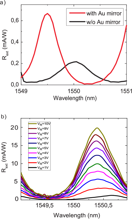
To confirm the cavity effect on PD responsivity, we measure with and without Au mirror, Fig.7a. The slight (0.5nm) variation in resonant wavelength (Fig.7a,b) is attributed to fabrication tolerances between different devices. We observe a 3-fold enhancement with the Au mirror compared to the bare Si/air interface, in good agreement with the simulations in Fig.2. To further enhance , we exploit the Schottky barrier lowering effect and apply a larger (up to 10V) reverse bias to the PDs with integrated Au mirrors. Fig.7b plots for different VR. We get 20mA/W at VR=10V, which corresponds to 0.25A/W, considering the 8 absorption in the SLG electrode. To the best of our knowledge, this is the highest value reported so far for vertically-illuminated Schottky Si PDs at 1550nm. may be further increased by integrating an antireflection coating to further enhance the SLG absorption.
In summary, we demonstrated a spectrally-selective, free-space illuminated SLG/Si Schottky PD at 1550nm. The photodetection mechanism is based on internal photoemission at the SLG/Si interface. The photodetection is enhanced by integration in a F-P cavity and increasing the SLG absorption due to multiple reflections at the cavity resonance. As a result, we showed wavelength-dependent photoresponse with external (internal) responsivity20mA/W (0.25A/W). The resonance wavelength may be further tuned by varying the Si cavity thickness while the spectral-selectivity can be increased by taking advantage of more complex high-finesse microcavities, which would provide both integrated spectral filtering and enhanced SLG absorption. Our devices pave the way for developing high-responsivity graphene-Si free-space illuminated PDs for for NIR.
We acknowledge funding from EU Graphene Flagship, ERC Grant Hetero2D, EPSRC Grants EP/K01711X/1, EP/K017144/1, EP/N010345/1, and EP/L016087/1.
References
- (1) G. P. Agrawal, Fiber-Optic Communication Systems (John Wiley & Sons, New York, 2010), 4th Edition.
- (2) E. Leitgeb, M. Gebhart and U. Birnbacher, J. Opt. Fiber. Comm. Rep. 2, 56 (2005).
- (3) H. Kaushal and G. Kaddoum, IEEE Commun. Surveys Tuts. 99, 1 (2016).
- (4) M. Ijaz, Z. Ghassemlooy, S. Rajbhandari, H. Le Minh, J. Perez and A. Gholami, Comparison of 830 nm and 1550 nm based Free Space Optical Communications link under Controlled Fog Conditions, (IEEE, 8th International Symposium on Communication Systems, Networks & Digital Signal Processing, 2012).
- (5) M. Flood, Photogramm. Eng. Remote Sensing 67, 1209 (2001).
- (6) C. E. Parrish and R. Osiri, Lidar Wavelength Considerations and Radiometric Performance Analysis for Coastal Applications, (American Geophysical Union, Fall Meeting, San Francisco, 2011)
- (7) S. Ishida and N. Nishizawa, Biomed. Opt. Express 3, 282 (2012).
- (8) S. M. Sze, K. K. Ng, Physics of Semiconductor Devices (John Wiley & Sons, New York, 2006), 3rd Edition.
- (9) P. C. Eng, S. Song and B. Ping, Nanophotonics 4, 277 (2015).
- (10) M. Casalino, L. Sirleto, L. Moretti, F. Della Corte and I. Rendina, J. Opt. A Pure Appl. Op. 8, 909 (2006).
- (11) Y. M. Kang, H. D. Liu, M. Morse, M. J. Paniccia, M. Zadka, S. Litski, G. Sarid, A. Pauchard, Y. H. Kuo, H. W. Chen et al., Nat. Photonics 3, 59 (2009).
- (12) G. Masini, V. Cencelli, L. Colace, F. De Notaristefani and G. Assanto, Appl. Phys. Lett. 80, 3268 (2002).
- (13) S. J. Koester, J. D. Schaub, G. Dehlinger and J. O. Chu, IEEE J. Sel. Top. Quantum Electron. 12, 1489 (2006).
- (14) J. Michel, J. F. Liu and L. C. Kimerling, Nat. Photonics 4, 527 (2010).
- (15) S. Assefa, F. N. A. Xia and Y. A. Vlasov, Nature 464, 80 (2010).
- (16) S. Y. Zhu, M. B. Yu, G. Q. Lo and D. L. Kwong, Appl. Phys. Lett. 92, 081103 (2008).
- (17) I. Goykhman, B. Desiatov, J. Khurgin, J. Shappir and U. Levy, Nano Lett. 11, 2219 (2011).
- (18) I. Goykhman, B. Desiatov, J. Khurgin, J. Shappir and U. Levy, Opt. Express 20, 28594 (2012).
- (19) M. Casalino, M. Iodice, L. Sirleto, S. Rao, I. Rendina and G. Coppola, J. Appl. Phys. 114, 153103 (2013).
- (20) A. Akbari, R. N. Tait and P. Berini, Opt. Express 18, 8505 (2010).
- (21) R. H. Walden, A review of recent progress in InP-based optoelectronic integrated circuit receiver front-ends, (GaAs IC Symposium IEEE Gallium Arsenide Integrated Circuit Symposium. 18th Annual Technical Digest, 1996).
- (22) Y. Kang, P. Mages, A. R. Clawson, P. K. L. Yu, M. Bitter, Z. Pan, A. Pauchard, S. Hummel and Y. H. Lo, IEEE Photon. Technol. Lett. 14, 1593 (2002).
- (23) S. M. Sze VLSI Technology (McGraw-Hill Education 2003), 2nd Edition.
- (24) J. H. Lau, Flip chip technologies (McGraw-Hill, New York, 1995)
- (25) D. L. Harame, S. J. Koester, G. Freeman, P. Cottrel, K. Rim, G. Dehlinger, D. Ahlgren, J. S. Dunn, D. Greenberg, A. Joseph et al., Appl. Surf. Sci. 224, 9 (2004).
- (26) J. A. Wang and S. Lee, Sensors 11, 696 (2011).
- (27) D. W. Peters, Proc. IEEE 55, 704 (1967).
- (28) M. L. Brongersma, N. J. Halas and P. Nordlander, Nat. Nanotechnol. 10, 25 (2015).
- (29) M. Casalino, IEEE J. Quant. Elecrton. 52, 4000110 (2016).
- (30) M. Kimata, M. Ueno, H. Yagi, T. Shiraishi, M. Kawai, K. Endo, Y. Kosasayama, T. Sone, T. Ozeki and N. Tsubouchi, Opto-Electron. Rev. 6, 1 (1998).
- (31) I. Goykhman, B. Desiatov, J. Shappir, J. B. Khurgin, U. Levy, arXiv:1401.2624.
- (32) M. Casalino, G. Coppola, R. M. De La Rue, D. F. Logan, Laser & Photonics Review 10, 895 (2016).
- (33) B. Desiatov, I. Goykhman, N. Mazurski, J. Shappir, J. B. Khurgin and U. Levy, Optica 2, 335 (2015).
- (34) M. Amirmazlaghani, F. Raissi, O. Habibpour, J. Vukusic and J. Stake, IEEE J. Quantum Electron. 49, 589 (2013).
- (35) X. M. Wang, Z. Z. Cheng, K. Xu, H. K. Tsang and J. B. Xu, Nat. Photonics 7, 888 (2013).
- (36) I. Goykhman, U. Sassi, B. Desiatov, N. Mazurski, S. Milana, D. De Fazio, A. Eiden, J. Khurgin, J. Shappir, U. Levy et al., Nano Lett. 16, 3005 (2016).
- (37) X. H. An, F. Z. Liu, Y. J. Jung and S. Kar, Nano Lett. 13, 909 (2013).
- (38) A. Di Bartolomeo, Phys. Report. 606, (2016).
- (39) C. C. Chen, M. Aykol, C. C. Chang, A. F. J. Levi and S. B. Cronin, Nano Lett. 11, 1863 (2011).
- (40) A. C. Ferrari, F. Bonaccorso, V. Fal’ko, K. S. Novoselov, S. Roche, P. Boggild, S. Borini, F. H. L. Koppens, V. Palermo, N. Pugno et al., Nanoscale 7, 4598 (2015).
- (41) F. H. L. Koppens, T. Mueller, P. Avouris, A. C. Ferrari, M. S. Vitiello and M. Polini, Nat. Nanotechnol. 9, 780 (2014).
- (42) F. Bonaccorso, Z. Sun, T. Hasan and A. C. Ferrari, Nat. Photonics 4, 611 (2010).
- (43) Z. P. Sun, T. Hasan, F. Torrisi, D. Popa, G. Privitera, F. Q. Wang, F. Bonaccorso, D. M. Basko and A. C. Ferrari, ACS Nano 4, 803 (2010).
- (44) V. Sorianello, M. Midrio, G. Contestabile, I. Asselberg, J. Van Campenhout, C. Huyghebaerts, I. Goykhman, A. K. Ott, A. C. Ferrari and M.Romagnoli, arXiv:1704.01525 (2017).
- (45) R. R. Nair, P. Blake, A. N. Grigorenko, K. S. Novoselov, T. J. Booth, T. Stauber, N. M. R. Peres and A. K. Geim, Science 320, 1308 (2008).
- (46) J. M. Dawlaty, S. Shivaraman, J. Strait, P. George, M. Chandrashekhar, F. Rana, M. G. Spencer, D. Veksler and Y. Q. Chen, Appl. Phys. Lett. 93, 131905 (2008).
- (47) M. A. Muriel and A. Carballar, IEEE Photon. Technol. Lett. 9, 955 (1997).
- (48) P. B. Johnson and R. W. Christy, Phys. Rev. B 6, 4370–4379 (1972).
- (49) L. A. Falkovsky, S. S. Pershoguba, Phys Rev B 76, 76.153410 (2007).
- (50) L. A. Falkovsky, A. A. Varlamov, Eur. Phys. J. B 56, 281 (2007).
- (51) H. H. Li, J. Phys. Chem. Ref. Data 9, (1993).
- (52) S. Bae, H. Kim, Y. Lee, X. F. Xu, J. S. Park, Y. Zheng, J. Balakrishnan, T. Lei, H. R. Kim, Y. I. Song et al., Nat. Nanotechnol. 5, 574 (2010).
- (53) A. A. Lagatsky, Z. Sun, T. S. Kulmala, R. S. Sundaram, S. Milana, F. Torrisi, O. L. Antipov, Y. Lee, J. H. Ahn, C. T. A. Brown, W. Sibbett, A. C. Ferrari, Appl. Phys. Lett. 102, (2013).
- (54) A. C. Ferrari, J. C. Meyer, V. Scardaci, C. Casiraghi, M. Lazzeri, F. Mauri, S. Piscanec, D. Jiang, K. S. Novoselov, S. Roth et al., Phys. Rev. Lett. 97, 187401 (2006).
- (55) A. C. Ferrari and D. M. Basko, Nat. Nanotechnol. 8, 235 (2013).
- (56) A. Das, S. Pisana, B. Chakraborty, S. Piscanec, S. K. Saha, U. V. Waghmare, K. S. Novoselov, H. R. Krishnamurthy, A. K. Geim, A. C. Ferrari et al., Nat. Nanotechnol. 3, 210 (2008).
- (57) M. Bruna, A. K. Ott, M. Ijas, D. Yoon, U. Sassi and A. C. Ferrari, ACS Nano 8, 7432 (2014).
- (58) P. A. Temple and C. E. Hathaway, Phys. Rev. B 7, 3685 (1973).
- (59) D. M. Basko, S. Piscanec and A. C. Ferrari, Phys. Rev. B 80, 165413 (2009).
- (60) L. G. Cancado, A. Jorio, E. H. Ferreira, F. Stavale, C. A. Achete, R. B. Capaz, M. V. Moutinho, A. Lombardo, T. S. Kulmala and A. C. Ferrari, Nano Lett. 11, 3190 (2011).
- (61) S. Tongay, M. Lemaitre, X. Miao, B. Gila, B. R. Appleton and A. F. Hebard, Phys. Rev. X 2, (2012).