Observation of two-dimensional Fermi surface and Dirac dispersion in YbMnSb2
Abstract
We present the crystal structure, electronic structure, and transport properties of the material YbMnSb2, a candidate system for the investigation of Dirac physics in the presence of magnetic order. Our measurements reveal that this system is a low-carrier-density semimetal with a 2D Fermi surface arising from a Dirac dispersion, consistent with the predictions of density functional theory calculations of the antiferromagnetic system. The low temperature resistivity is very large, suggesting scattering in this system is highly efficient at dissipating momentum despite its Dirac-like nature.
I Introduction
The coexistence of topological band structures and more conventional broken symmetry orders has yet to be investigated extensively, primarily due to the lack of suitable materials systems. As a result, several studies have focused on the structural family RMnPn2, where R is a rare-earth metal and Pn is a pnictide (usually Sb or Bi),Wang and Petrovic (2012); Guo et al. (2014); Jo et al. (2014); May et al. (2014); Farhan et al. (2014); Liu et al. (2015) due to the possible coexistence of protected band crossings and magnetic order on the Mn sublattice. The magnetic order is thought to be antiferromagnetic, breaking the spin degeneracy of the system, and it has been argued that this leads to crossings separated in energy in the band structure.Zyuzin et al. (2012); Borisenko et al. (2015); Wang et al. (2016a) Two members of this family, SrMnBi2 and YbMnBi2, have been proposed as possible topological semimetals hosting magnetic order,Jo et al. (2014); Wang et al. (2016b) but comparatively little work has investigated their Sb-based cousins.Huang et al. (2017) We have synthesized a new member of this family, YbMnSb2, and report here comprehensive transport and spectroscopic measurements. Evidence from Shubnikov-de Haas oscillations and angle-resolved photoemission spectroscopy (ARPES) suggest there is at least one 2D Fermi surface of Dirac origin. The ARPES data is in agreement with density functional theory (DFT) calculations of the antiferromagnetic band structure, which indicates that YbMnSb2 may therefore be a new topological material in the presence of magnetic order. However, despite the observation of quantum oscillations, the low temperature resistivity of these materials is large, suggesting that quantum and transport lifetimes have the same origin in these materials.
II EXPERIMENT
II.1 Crystal synthesis and structure
Single crystals of YbMnSb2 were synthesized using a tin-flux technique. Ytterbium (99.9%), manganese (99.95%), antimony (99.9999%), and tin (99.999%), all from Alfa Aesar, were mixed in the mole ratio 1:1:4:10 (Yb:Mn:Sb:Sn). The mixture was placed in an alumina crucible and sealed in an evacuated quartz ampule, then heated over 8 h to 1050°C where it dwelled for 24 h. Next, the ampule was cooled to 600°C over 100 h, and then centrifuged to remove excess tin. This process yielded single crystals of approximately 1 mm 1 mm 0.05 mm.
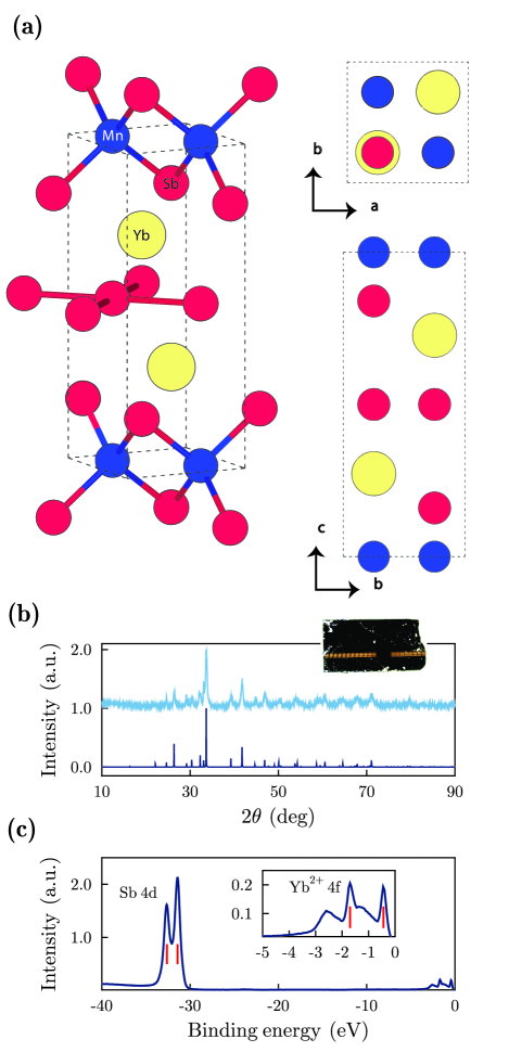
The crystallographic parameters are listed in Table 1 and the atomic coordinates and displacement parameters are provided in Table 2. The crystal structure is shown schematically in Fig. 1(a). Single crystals of YbMnSb2 were cut to an appropriate size and mounted on a glass fiber using epoxy. The fiber was mounted on a Bruker D8 Quest Kappa single-crystal X-ray diffractometer with a Mo K IS microfocus source (Å) operating at 50 kV and 1 mA, a HELIOS optics monochromator, and a CMOS detector. The Bruker program sadabs (multi-scan method) was used to correct the collected data for absorption. A starting model of YbMnSb2 was obtained using the intrinsic phasing method in shelxt.Sheldrick (2015a) Atomic sites were refined anisotropically using shelxl2014.Sheldrick (2015b) Figure 1(b) shows a characteristic powder pattern (collected using Cu radiation on a Rigaku Ultima IV powder diffractometer) together with the simulated powder pattern, computed in vesta.Momma and Izumi (2011) Core-level spectroscopy on the merlin beamline (see Sec. II-C) confirms the divalent oxidation state of Yb (Fig. 1(c)).
YbMnSb2 belongs to the tetragonal, centrosymmetric P4/nmm space group and is isotypic with the HfCuSi2 structure type.Andrukhiv et al. (1975) YbMnSb2 does not exhibit a Mn deficiency that is observed in compounds of the same structure type with larger rare earth elements, e.g. LnMn1-xSb2 (Ln = La, Ce, Pr, Nd, or Sm).Wollesen et al. (1996) The independent confirmation of the YbMnSb2 crystal structure allows for a first-principles calculation of the electronic band structure, which we consider next.
| Crystal type | YbMnSb2 |
|---|---|
| space group | P4/nmm, #129 |
| a, c (Å) | 4.3215(17), 10.828(4) |
| V (Å3) | 202.22(17) |
| Z | 2 |
| temperature (K) | 300 |
| range (°) | 3.8–30.7 |
| (mm-1) | 38.93 |
| measured reflections | 1085 |
| independent reflections | 224 |
| 0.033 | |
| (e Å-3) | 1.64 |
| (e Å-3) | -3.56 |
| GOF | 1.27 |
| 111 | 0.033 |
| 222 | 0.060 |
| YbMnSb2 | Wyckoff site | x | y | z | (Å2) |
| Yb | 2c | 0.72728(8) | 0.0106(2) | ||
| Mn | 2a | 0 | 0.0115(6) | ||
| Sb 1 | 2b | 0.0115(3) | |||
| Sb 2 | 2c | 0.15995(12) | 0.0099(3) |
II.2 Electronic structure
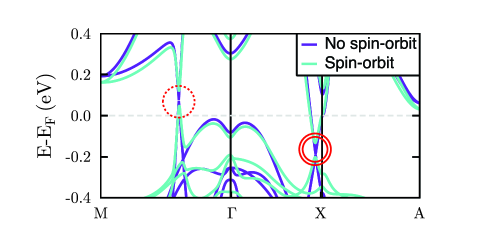
Using the lattice parameters using the measured structural data reported in Table 1 and Table 2, we performed spin-polarized density functional calculations within the generalized gradient approximation (GGA) using the Vienna ab initio Simulation Package (vasp).Kresse and Furthmüller (1996); Kresse and Hafner (1993) We used the projector augmented wave (PAW) method, treating explicitly 5s, 5p, 4f, and 6s for Yb; 3d and 4s for Mn; and 5s and 5p for Sb. Wavefunctions were expanded in a plane wave basis up to an energy cutoff of 600 eV. We used Monkhorst-Pack -point grids of for Brillouin zone sampling.Monkhorst and Pack (1976) Spin-orbit coupling was neglected except when computing the band structure in Fig. 2 and when identifying the magnetic easy axis. We used the PBE GGA functionalPerdew et al. (1996) with Hubbard correctionsDudarev et al. (1998) for the Yb 4f states, where we used a of 4 eV. This value of was chosen to best reproduce the photoemission data, which placed the Yb 4f states at eV below the Fermi energy. We did not include a Hubbard for the Mn 3d electrons after tests indicated such a had no effect on the electronic structure near the Fermi level.
All calculations assumed antiferromagnetic (AFM) order for the spins on the Mn sites, with the two Mn ions in each cell having opposite spin. This AFM ordering was calculated to be 0.23 eV and 2.62 eV per formula unit lower in energy than ferromagnetic order and a non-spin-polarized calculation, respectively. We compute the magnetic easy axis to be in-plane, and 1 meV/f.u. lower in energy than for out-of-plane spin orientations.
The band structure is shown in Fig. 2. Note the linear band crossings on the -M and -X lines. The calculated Fermi surface is displayed in Fig. 3, showing 2D and 3D Fermi surface pockets.
II.3 Angle-resolved photoemission spectroscopy
To experimentally investigate the electronic structure of YbMnSb2, we performed ARPES measurements at the MERLIN beamline 4.0.3 of the Advanced Light Source, employing both linear horizontal and linear vertical polarization from an elliptically polarized undulator. The experiment used a Scienta R8000 electron spectrometer with 2D parallel detection of electron kinetic energy and angle in combination with a highly-automated six-axis helium cryostat goniometer with 6 K base temperature operating in low 10-11 torr pressure. The energy resolution of these measurements was approximately 10–20 meV. These results are presented in Fig. 3 and Fig. 4.
II.4 DFT/ARPES comparison
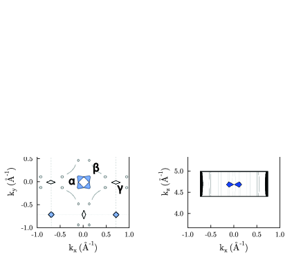
Figure 3(a) shows a Fermi surface (FS) map obtained by integrating ARPES intensity inside a 20 meV energy window around the Fermi energy (), measured with photon energy 78 eV. There are three distinct regions with high photoemission intensities: a 3D FS centered at the point (), a small 2D hole pocket along the -X line (), and a skinny, 2D banana-like pocket on the -M line (). To compare the data with the calculation, we plot the Fermi surface as calculated by DFT in Fig. 3(b). This calculation shows all three of these features. The lack of fourfold symmetry in the data (Fig. 3(a)) as compared with the calculated FS (Fig. 3(b)) is due to selection rules arising from the photon polarization.
Figure 3(c) shows the photon-energy dependent -maps from 50–120 eV of the ARPES intensity at , cut along the -X high-symmetry line (yellow dashed line in Fig. 3(a)). The Fermi-edge - photon-energy dependent maps show 2D behavior for the X-point pocket (), but 3D -dispersive behavior near point (pocket ). These features are reported in related compounds: The 2D state was observed in YbMnBi2Borisenko et al. (2015) which was attributed to the Yb-Bi plane, and 3D behavior has been reported in LaAgSb2, and attributed to the Sb plane. Shi et al. (2016)
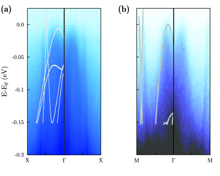
ARPES intensity plots along the M--M and X--X lines are shown in Fig. 4. The calculated bands in each cut are overlaid on the ARPES data to show the robust agreement between the experiment and the calculation. Note the presence of a hole pocket in panel (a) and an electron pocket in panel (b), both with linear dispersion.
II.5 Transport and Hall effect
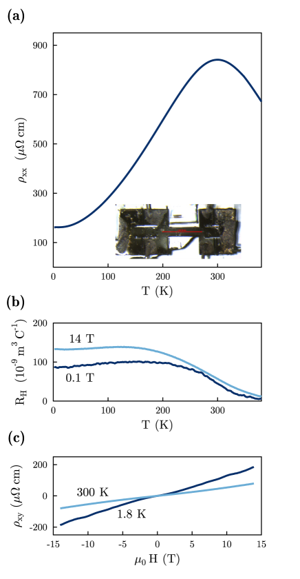
Single crystals were contacted by sputtering gold in the desired configuration and attaching annealed platinum wires with silver paste (Dupont 4929N). After contacting, the sample was shaped into a “Hall bar” geometry using a plasma focused ion beam (FIB). The resistance and magnetoresistance measurements were performed in a Quantum Design Physical Properties Measurement System (PPMS).
Figure 5(a) shows as a function of temperature. The non-monotonic temperature dependence of the resistivity could indicate a crossover between metallic and semiconducting behavior. It is unclear that this peak is associated with a true phase transition as its position varies between samples by over 20 K. The plot of Hall coefficient (Fig. 5(b)) as a function of temperature was constructed by antisymmetrizing data at T and T. The latter trace captures the high-field Hall coefficient, and the former trace approximately reflects the low-field Hall coefficient. Above K, nonlinearity in the Hall effect has vanished and the two traces converge.
At high fields (), the Hall coefficient of a multiband system is inversely related to the degree of compensation, according to
| (1) |
where is the total hole density and is the total electron density.Kohler (1949) We observe a reduction of the Hall coefficient with increasing temperature, which could reflect a reduction in the degree of compensation (assuming the high field limit is reached by 14 T, at 1.8 K, cm-3 while at 390 K cm-3). However, it is likely that the high field limit is not reached at high temperatures, so this change arises from a combination of the availability of thermally excited carriers and changing mobilities of electron and hole pockets.
A simple two-band low-field form of the effective carrier density predicts that this effective carrier density is dominated by high mobility carriers, according to
| (2) |
where is each carrier’s respective mobility. Band structure and photoemission both indicate that three bands may be present at the Fermi level, but qualitatively this two-band model shows that the Hall coefficient is determined by the highest mobility carrier. At low temperature, then, the 0.1 T trace (representing the low-field limit) shows the presence of high-mobility holes.
II.6 Shubnikov-de Haas measurements
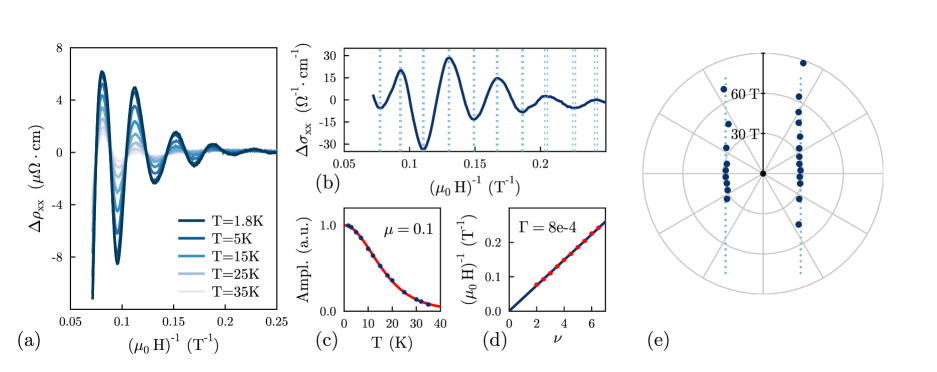
We observed Shubnikov-de Haas (SdH) oscillations in magnetic fields of up to 14 T at temperatures between 1.8 K and 35 K. Our results (Fig. 6) indicate that the Fermi surface is small (perpendicular area approximately 0.1% of the bulk Brillouin zone), strongly anisotropic, and the effective mass is small ().
Raw resistance versus field traces are processed in several steps. First, we subtract a best-fit fourth-order polynomial background from the trace. (For the frequencies observed, the results are largely insensitive to the order of polynomial background subtracted.) Our background-subtracted traces are plotted against inverse field () in Fig. 6(a). The background-free data is Fourier transformed against the inverse field to confirm the oscillation frequency.
In the absence of magnetic breakdown and other high-field effects, the oscillation frequencies observed are proportional to the areas of extremal orbits on the Fermi surface, in the plane normal to the applied field. Explicitly,
| (3) |
where is the oscillation frequency and the (-space) extremal area.
The SdH effect appears intrinsically as an oscillatory component of the conductivity, which we are able to obtain by simultaneous measurements of Hall and longitudinal resistance. Then can be calculated according to
| (4) |
and is shown in Fig. 6(b).
The SdH oscillation amplitude decays with temperature according to the Dingle form
| (5) |
with
| (6) |
Here is the harmonic index of the specific oscillation, is the cyclotron effective mass in units of the electron mass, and are the temperature and magnetic field, and is the bare electron mass.Lifshitz and Kosevich (1958)
In Fig. 6(c) we fit our data to Eq. 5, including a small offset arising from imperfect background subtraction, and we find that . (The amplitude plotted is the amplitude of the peak at approximately 10.45 T after background subtraction.) This mass is comparable to that observed in other topological systems, including Cd3As2,He et al. (2014) TaAs,Zhang et al. (2017) and Na3Bi.Kushwaha et al. (2015)
The SdH oscillation amplitude also decays with due to the effect of finite carrier relaxation times according to the formula
| (7) |
where is called the Dingle temperature, and is inversely related to the relaxation time
| (8) |
Shoenberg (1984)
Combining the oscillation frequency in Fig. 6(a) with the effective mass from Fig. 6(b) allows us to compute the various values in Table 3. Our reported oscillation frequency represents a Fermi-surface cross-sectional area of only 0.1% of the perpendicular Brillouin zone area Å-2.
The so-called Landau level fan diagram is frequently employed to measure the Berry’s phase in suspected topological systems. Conductivity minima in SdH oscillations (Fig. 6(b)) are plotted against their associated Landau level index. The -intercept of a linear fit to this data identifies the phase of the oscillations, and, in principle, the Berry’s phase accumulated around one cyclotron orbit, according to the relation
| (9) |
in which is the -intercept, the Berry’s phase, and a number less than 1/8 in magnitude.Sergelius et al. (2016); Luk’yanchuk and Kopelevich (2006); Cao et al. (2015); Luk’yanchuk and Kopelevich (2004); Pariari et al. (2015) Some authors suggest that is related to Fermi surface curvature: a smooth, 2D cylinder yields , but a “corrugated 3D Fermi surface” merits .Luk’yanchuk and Kopelevich (2004) The angular dependence of the oscillation frequency (Fig. 6(e) and discussed below) indicates our system is close to the 2D cylinder case, suggesting . In this case, a topologically nontrivial Berry’s phase of yields , while a trivial Berry’s phase of 0 yields . The actual value we measure in Fig. 6(d) is . This value indicates that the Fermi surface pocket we probe with SdH oscillations is consistent with having a topological origin.
| Parameter | Value |
|---|---|
| (T) | |
| (nm-1) | |
| (me) | |
| (cm-3) | |
| (K) |
By measuring SdH oscillations at different angles of the applied field, we are able to use the angular variation of the oscillation frequency to map the shape of the Fermi surface. The angular dependence of the SdH frequency is shown in Fig. 6(e), with a 5° sample positioning error subtracted. (After about 75° the oscillation amplitude has decreased in amplitude beyond detection.) Note that for a spherical Fermi surface, the data points in Fig. 6(e) would fall on a circle. Instead, they more closely follow a dependence consistent with a two-dimensional or strongly anisotropic three-dimensional Fermi surface.
III DISCUSSION
The angular dependence of the Shubnikov-de Haas oscillation frequency is consistent with a small 2D Fermi surface. This result is commensurate with our ARPES measurements, which show small 2D pockets along the and directions in the Brillouin zone. Moreover, both ARPES and the Landau level fan diagram suggest that these pockets originate from a Dirac band crossing. YbMnSb2 may therefore be a new topological material.
ARPES and DFT calculations indicate that three Fermi surface pockets contribute carriers: (1) Small 3D hole-like pockets (), with a large effective mass, (2) 2D electron-like cylinders (), with a small effective mass, and (3) small 2D hole-like elliptic cylinders (), also with a small effective mass.
Using the SdH oscillation data in Table 3, we can place an upper bound on the low temperature resistivity with a simple Drude approximation for a single pocket. This value is an upper bound both because the Dingle lifetime is sensitive to small-angle scattering (which only weakly affects the resistance) and because it ignores all other Fermi pockets.Shoenberg (1984) Assuming a cylindrical Fermi surface, this bound is , with the uncertainty primarily arising from the determination of the Dingle lifetime. Our observed resistivity at low temperature is , which nearly coincides with this upper bound. (The uncertainty in this resistivity originates from the measurement of the sample thickness.) This observation would imply that YbMnSb2 is in an unusual case whereby the quantum lifetime matches the transport lifetime. There are two plausible explanations for this. The first is that, the quantum oscillations we observe do not originate from bulk bands but in fact originate from high mobility surface states that carry most of the current. However, our preliminary studies show that there is a weak thickness dependence to the resistivity, suggesting surface states do not contribute significantly to the current.
The second scenario is that, although the quantum (Dingle) lifetime tends to underestimate the transport (Drude) lifetime due to its sensitivity to small-angle scattering, the Fermi surface in this material is quite small and so small-angle scattering may be catastrophic, hence efficiently dissipating momentum. The remainder of the carriers must then have very low mobility, and contribute relatively little to conduction having been “shorted out” by the mobile carriers observed in quantum oscillations. In this scenario, the SdH oscillations must originate from either the 2D or pockets since the pockets can be ruled out because they are 3D. The Hall effect (Fig. 5(c)) indicates that hole-like carriers are more numerous and more mobile, suggesting the pocket is the origin of these oscillations. On the other hand, the balance of carriers and mobilities may conspire to achieve an identical Hall signal such that the pockets cannot be ruled out. Nevertheless, the balance of evidence suggests this second scenario most likely explains our data.
Finally, we emphasize that our ARPES data cannot be reconciled with our DFT calculations without antiferromagnetic order on the Mn sites. Thus, although we do not have any direct thermodynamic evidence for an antiferromagnetic phase transition, the close agreement between the calculations and experiment strongly suggests the presence of magnetic order. It may be that the thermodynamic anomaly is weak and cannot be resolved, or occurs at temperatures beyond those measured here. Compounds with identical Mn sublattices, including EuMnBi2 ( 310 K)May et al. (2014) and SrMnBi2 ( 290 K),Park et al. (2011) exhibit antiferromagnetic ordering near room temperature.
IV Conclusion
We have performed a comprehensive study of the candidate topological semimetal YbMnSb2 using electrical transport and ARPES measurements, all of which can be reconciled with our detailed DFT calculations. Shubnikov-de Haas oscillations reveal a 2D Fermi surface of Dirac origin, as predicted by DFT and consistent with ARPES measurements. This work indicates that YbMnSb2 is a possible new test bed for the study of topological states of matter in the presence of broken-symmetry order.
V Acknowledgments
R. K. is supported by the National Science Foundation (NSF) Graduate Research Fellowship under Grant No. DGE-1106400. S. J., C. J., J. G. A., and much of this work received support from the Gordon and Betty Moore Foundation under Grant No. GBMF4374. S. J., S. M. G., J. D. D. and J. B. N. were supported by the Director, Office of Science, Office of Basic Energy Sciences, Materials Sciences and Engineering Division, of the U.S. Department of Energy under Contract No. DE-AC02-05-CH11231. Computational resources provided in part by the Molecular Foundry were supported by the Office of Science, Office of Basic Energy Sciences, of the U.S. Department of Energy, also under Contract No. DE-AC02-05-CH11231. S. M. G. acknowledges financial support by the Swiss National Science Foundation Early Postdoctoral Mobility Program. K. A. B. and J. Y. C. acknowledge partial support from NSF DMR-1360863. This paper also benefited from Dr. Nicholas P. Breznay’s constructive feedback.
References
- Wang and Petrovic (2012) K. Wang and C. Petrovic, Phys. Rev. B 86, 155213 (2012).
- Guo et al. (2014) Y. F. Guo, A. J. Princep, X. Zhang, P. Manuel, D. Khalyavin, I. I. Mazin, Y. G. Shi, and A. T. Boothroyd, Physical Review B 90, 075120 (2014).
- Jo et al. (2014) Y. Jo, J. Park, G. Lee, M. J. Eom, E. Choi, J. H. Shim, W. Kang, and J. S. Kim, Physical Review Letters 113, 156602 (2014).
- May et al. (2014) A. F. May, M. A. McGuire, and B. C. Sales, Physical Review B 90, 075109 (2014).
- Farhan et al. (2014) M. A. Farhan, G. Lee, and J. H. Shim, Journal of Physics: Condensed Matter 26, 042201 (2014).
- Liu et al. (2015) J. Y. Liu, J. Hu, D. Graf, S. M. A. Radmanesh, D. J. Adams, Y. L. Zhu, G. F. Chen, X. Liu, J. Wei, I. Chiorescu, L. Spinu, and Z. Q. Mao, arXiv:1507.07978 [cond-mat] (2015), arXiv: 1507.07978.
- Zyuzin et al. (2012) A. A. Zyuzin, S. Wu, and A. A. Burkov, Physical Review B 85, 165110 (2012).
- Borisenko et al. (2015) S. Borisenko, D. Evtushinsky, Q. Gibson, A. Yaresko, T. Kim, M. N. Ali, B. Büchner, M. Hoesch, and R. J. Cava, arXiv:1507.04847 [cond-mat] (2015), arXiv: 1507.04847.
- Wang et al. (2016a) Z. Wang, M. Vergniory, S. Kushwaha, M. Hirschberger, E. Chulkov, A. Ernst, N. Ong, R. J. Cava, and B. A. Bernevig, Physical Review Letters 117, 236401 (2016a).
- Wang et al. (2016b) A. Wang, I. Zaliznyak, W. Ren, L. Wu, D. Graf, V. O. Garlea, J. B. Warren, E. Bozin, Y. Zhu, and C. Petrovic, Physical Review B 94, 165161 (2016b).
- Huang et al. (2017) S. Huang, J. Kim, W. A. Shelton, E. W. Plummer, and R. Jin, Proceedings of the National Academy of Sciences 114, 6256 (2017).
- Sheldrick (2015a) G. M. Sheldrick, Acta Crystallographica Section A Foundations and Advances 71, 3 (2015a).
- Sheldrick (2015b) G. M. Sheldrick, Acta Crystallographica. Section C, Structural Chemistry 71, 3 (2015b).
- Momma and Izumi (2011) K. Momma and F. Izumi, Journal of Applied Crystallography 44, 1272 (2011).
- Andrukhiv et al. (1975) L. Andrukhiv, L. Lysenko, Y. Yarmolyuk, and E. Gladyshevskii, Dopovidi Akademii Nauk Ukrains’koi RSR, Seriya A: Fiziko-Tekhnichni ta Matematichni Nauki 1975, 645 (1975).
- Wollesen et al. (1996) P. Wollesen, W. Jeitschko, M. Brylak, and L. Dietrich, Journal of Alloys and Compounds 245, L5 (1996).
- Kresse and Furthmüller (1996) G. Kresse and J. Furthmüller, Phys. Rev. B 54, 11169 (1996).
- Kresse and Hafner (1993) G. Kresse and J. Hafner, Phys. Rev. B 48, 13115 (1993).
- Monkhorst and Pack (1976) H. J. Monkhorst and J. D. Pack, Phys. Rev. B 13, 5188 (1976).
- Perdew et al. (1996) J. P. Perdew, K. Burke, and M. Ernzerhof, Phys. Rev. Lett. 77, 3865 (1996).
- Dudarev et al. (1998) S. L. Dudarev, G. A. Botton, S. Y. Savrasov, C. J. Humphreys, and A. P. Sutton, Phys. Rev. B 57, 1505 (1998).
- Shi et al. (2016) X. Shi, P. Richard, K. Wang, M. Liu, C. E. Matt, N. Xu, R. S. Dhaka, Z. Ristic, T. Qian, Y.-F. Yang, C. Petrovic, M. Shi, and H. Ding, Phys. Rev. B 93, 081105 (2016).
- Kohler (1949) M. Kohler, Annalen der Physik 440, 99 (1949).
- Lifshitz and Kosevich (1958) I. M. Lifshitz and L. M. Kosevich, Journal of Experimental and Theoretical Physics 33, 88 (1958).
- He et al. (2014) L. P. He, X. C. Hong, J. K. Dong, J. Pan, Z. Zhang, J. Zhang, and S. Y. Li, Physical Review Letters 113, 246402 (2014).
- Zhang et al. (2017) C.-L. Zhang, Z. Yuan, Q.-D. Jiang, B. Tong, C. Zhang, X. C. Xie, and S. Jia, Physical Review B 95, 085202 (2017).
- Kushwaha et al. (2015) S. K. Kushwaha, J. W. Krizan, B. E. Feldman, A. Gyenis, M. T. Randeria, J. Xiong, S.-Y. Xu, N. Alidoust, I. Belopolski, T. Liang, M. Z. Hasan, N. P. Ong, A. Yazdani, and R. J. Cava, APL Materials 3, 041504 (2015).
- Shoenberg (1984) D. Shoenberg, Magnetic oscillations in metals, Cambridge monographs on physics (Cambridge University Press, Cambridge [Cambridgeshire] ; New York, 1984).
- Sergelius et al. (2016) P. Sergelius, J. Gooth, S. Bäßler, R. Zierold, C. Wiegand, A. Niemann, H. Reith, C. Shekhar, C. Felser, B. Yan, and K. Nielsch, Scientific Reports 6 (2016), 10.1038/srep33859.
- Luk’yanchuk and Kopelevich (2006) I. A. Luk’yanchuk and Y. Kopelevich, Physical Review Letters 97, 256801 (2006).
- Cao et al. (2015) J. Cao, S. Liang, C. Zhang, Y. Liu, J. Huang, Z. Jin, Z.-G. Chen, Z. Wang, Q. Wang, J. Zhao, S. Li, X. Dai, J. Zou, Z. Xia, L. Li, and F. Xiu, Nature Communications 6, 7779 (2015).
- Luk’yanchuk and Kopelevich (2004) I. A. Luk’yanchuk and Y. Kopelevich, Physical Review Letters 93, 166402 (2004).
- Pariari et al. (2015) A. Pariari, P. Dutta, and P. Mandal, Physical Review B 91, 155139 (2015).
- Park et al. (2011) J. Park, G. Lee, F. Wolff-Fabris, Y. Y. Koh, M. J. Eom, Y. K. Kim, M. A. Farhan, Y. J. Jo, C. Kim, J. H. Shim, and J. S. Kim, Physical Review Letters 107, 126402 (2011).