Edge enhanced growth induced shape transition in the formation of GaN Nanowall Network
Abstract
We address the mechanism of early stages of growth and shape transition of the unique nanowall network (NwN) nanostructure of GaN by experimentally monitoring its controlled growth using PA-MBE and complementing it by first-principles calculations. Using electron microscopy, we observe the formation of tetrahedron shaped (3 faced pyramid) islands at early stages of growth, which later grows anisotropically along their edges of the (201) facets, to form the wall like structure. The mechanism of this crystal growth is discussed in light of surface free energies of the different surfaces, adsorption energy and diffusion barrier of Ga ad-atoms on the (201) facets. By first-principles calculations, we find that the diffusion barrier of ad-atoms decreases with decreasing width of facets, and is responsible for the anisotropic growth and formation of the nanowall network. This study suggest that formation of NwN is a archetype example of structure dependent attachment kinetic (SDAK) instability induced shape transition in thin film growth.
pacs:
I Introduction
The dynamics of shape transitions plays a critical role in the evolution of surface morphology and uniformity of hetero-epitaxial thin film and nanostructure growth.Rastelli et al. (2001); Barth et al. (2005); Tersoff and Tromp (1993); Brune et al. (1998); Consonni et al. (2010). Critical to success of such nanostructure, especially while it is forming spontaneously, is the flexibility of the structure. However, lack of understanding on the role of attachment kinetics of adatoms and thermodynamic factors to the self assembly and the shape transitions is the major obstacle in achieving control over the growth of such structures. Therefore, investigations of the growth process of nanostructures enable us, to gain high control over the self-assembly. Further, the evolution of a structure from the early stages to the final morphology it attains is a very interesting and complex phenomena as many physical parameters compete with each other Shchukin and Bimberg (1999); Li et al. (2014); Pimpinelli and Villain (1998).
III-Nitrides (InN, GaN and AlN) are very special within semiconductors because of their applications in many areas due to direct and tunable band gap, mechanical and chemical stability, etcSang et al. (2013). Due to lack of availability of suitable native substrate, III-nitride films are typically grown on foreign substrates such as Sapphire, Silicon and Silicon carbide which results in formation of large density of defectsLi et al. (2016), which degrades crystalline quality of the material and consequently the device performance. To overcome this problem, different growth techniques have been employed in the past, among which use of nanostructures is efficient and cost effectiveFeng (2017); Himwas (2015).
Various morphological nanostructures of III-nitride (especially GaN) have been reported Kuykendall et al. (2003); Zhou et al. (2003); Colby et al. (2010), out of which the porous structure of GaN has shown great potential for various applicationsSoh et al. (2013); Yam and Hassan (2007); Föll et al. (2006). Most of the growth of porous GaN is achieved by top down approaches such as chemical etchingWang et al. (2004) or ion bombardment Lian et al. (2006), which limit the device performance due to contamination, undesired interface and defect states, and degradation in crystallinity and composition. Previously, we have shown that by controlling V/III ratio, spontaneous formation of porous nanostructures can be achieved by using PA-MBE system,Thakur et al. (2015); Nayak et al. (2017); Kesaria and Shivaprasad (2011); Thakur and Shivaprasad (2015); Kesaria and Shivaprasad (2011) which was followed by a few groups Zhong and Hane (2012, 2013); Poppitz et al. (2014); Kushvaha et al. (2017). Investigations of the growth process of NwN are highly important to control shape and size of the pores, to enhance light extraction efficiencyNayak et al. (2017). Poppitz et al. Poppitz et al. (2014) carried out a thickness dependent study of porous GaN on 6H-SiC, where they found that the islands laterally elongate to form a network like structure. Further, Wu et al.Wu et al. (2009) demonstrated a similar pathway for the growth of ZnO nanowall grown on Sapphire substrate by Metal-Organic Chemical Vapour Deposition (MOCVD). Both these reports show step-wise evolution of the morphology, but no clear mechanism was proposed in either case. We intend to monitor the shape transition of the NwN that occur during the initial stage of the growth as it plays a crucial role in determining the final morphology of thin films and nanostructuresRastelli et al. (2001); Barth et al. (2005); Tersoff and Tromp (1993); Brune et al. (1998); Consonni et al. (2010). In this report, we elucidate on growth mechanism of GaN NwN on Sapphire substrate by experimentally monitoring the evolution of surface morphology at intermediate stages of growth, complementing it by using first-principles Density Functional Theory (DFT) simulations. We find that the shape transition for this unique nanostructure of GaN from intial 3D island is driven by Structure Dependent Attachment Kinetics (SDAK) induced instability a.k.a edge sharpening instability (ESI), which was previously used to understand the growth of snow crystal by Libbrecht et. alLibbrecht (2011, 2012, 2017). We have undertaken this complementary study of experiment and calculations to correlate such instability induced growth mechanism of thin films and/or nanostructures.
II Methods
II.1 Experimental Details
The GaN films were grown under nitrogen rich conditions by using radio frequency Plasma Assisted Molecular Beam Epitaxy system (RF-PAMBE, SVTA-USA) over bare c-plane of Sapphire with base pressure of 310-11 Torr. The detailed procedure of substrate preparation can be found elsewhereKesaria and Shivaprasad (2011). Substrate temperature of 630 oC and plasma forward power of 375W were maintained for all samples grown for this work. The other growth parameters are listed in Table 1. The film structure was monitored in-situ by reflection high energy electron diffraction (RHEED) with an acceleration voltage of 7 kV, the morphology was determined ex-situ by field emission scanning electron microscope (FESEM) with an acceleration voltage of 20 kV and atomic force microscopy (AFM) in contact mode.
| Sample | Ga-K cell | N2 flow | Duration |
|---|---|---|---|
| Name | temp (oC) | rate (sccm) | (minute) |
| A | 1030 | 4.5 | 10 |
| B | 1030 | 4.5 | 20 |
| C | 1030 | 4.5 | 40 |
| D | 1030 | 4.5 | 60 |
| E | 1030 | 4.5 | 80 |
II.2 Simulation Details
Adsorption energy of Ga ad-atom on (201) surface is estimated by total energy calculation using first-principles Density Functional Theory (DFT), as implemented in the SIESTA codeSoler et al. (2002). Generalized Gradient Approximation (GGA) proposed by Perdew et al.Perdew et al. (1996) is used for the exchange and correlation function. We use the norm- conserving pseudopotentials of Troullier and Martins, with valence electron configurations of Gallium, Nitrogen, and Hydrogen as 3d10 4s2 4p1, 2s2 2p3 and 1s1, respectively. A double zeta basis set with polarization functions is used for all atoms. Hartree and exchange correlation energies are evaluated on a uniform real-space grid of points with a defined maximum kinetic energy of 200 Ry. Brillouin Zone of w-GaN is sampled on a - centered 553 mesh of k-points in the unit cell of reciprocal spacePack and Monkhorst (1977). Positions of all the atoms are allowed to relax by the conjugate gradient technique to optimize energy until forces on each atom is less than 0.04 eV/Å. The optimized lattice parameters of the unit cell are ‘a’ = 3.25 Å and ‘c’ = 5.23 Å. We construct a replica of the edge of the pyramid embedded with (201) surface, which makes an angle 75o with c-plane. A vacuum of 15 Å is added along all three axes to minimize the interaction of image configuration. The bottom layer and surface atoms, except the ones at (201) facets, were passivated with Hydrogen (see Fig. 3(c)). The adsorption energy of Ga on different sites of (201) surface is estimated by the equation
where is the total energy of the combined system with Ga ad-atoms and the wedge shape, , is the total energy of the pristine wedge and is the total energy of -Ga. The potential energy surface (PES) is constructed by placing Ga ad-atoms at various sites and allowing them to relax along the perpendicular to the (201) surface.
III Results
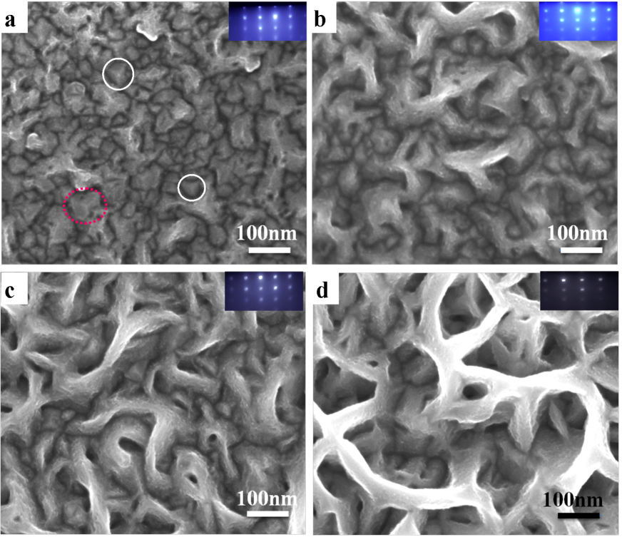
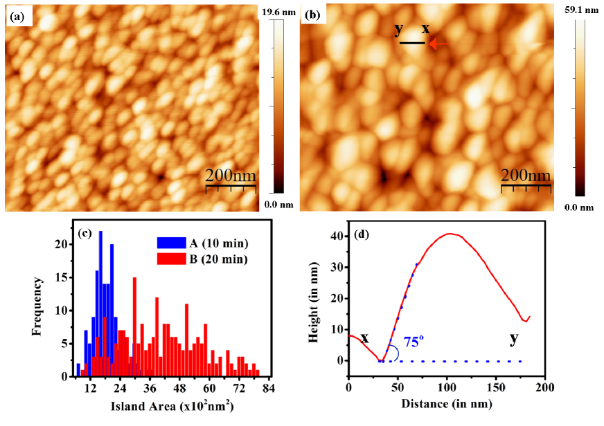
To look at the initial nucleation and evolution of surface morphology, we carry out growth of GaN NwN for durations of 10, 20, 40, 60 and 80 minutes. The corresponding FESEM images of the resulting morphology are shown in Fig.1. A careful visualization of the FESEM image of sample B shows formation of tetrahedron shaped faceted island structures (3 faced pyramids) (see inside the white circle of Fig.1 (a)). Along with these individual islands, we also observe a few Y-shaped structures (see inside red circle of Fig.1 (a)). Sample C, grown for higher duration (40 min) shows mostly Y-shaped structures with a few tetrahedron islands. Further, the length of tails of Y-shaped structure for sample B are 45-55 nm while for sample C they are longer ( 55-75 nm). Such increase in length of the tail of the Y-shaped structure with increased growth durations suggests that enhanced growth of the edges is responsible for the Y-shaped morphology. However, not all Y-shaped islands are connected to each other in both samples B and C. For samples grown for higher duration (samples D and E), we observe the Y- shaped structures connect with each other to form wall like features. To further look at earlier stage of island formation, we grow a film for 10 minutes under identical growth conditions. Fig.2 (a) and (b) shows the AFM image of samples A and B, respectively. At this early stage of growth (10 mins), we observe the formation of mostly oval shaped 3D islands with a large density ( 3.24 cm-2, see Fig.2 (a)). The island size distribution is plotted in Fig.2(c) where we find that the island sizes have a relatively uniform distribution with mean area 1900 nm2 with a standard deviation of 550 nm2. However, with increase in the deposition time to 20 minutes, size of most islands increases while that of a few ( 1.05 cm-2) remains unchanged (see Fig.2(c)), which results in a broad distribution of island sizes ( 1200-8000 nm2). It is very clear from SEM and AFM images, that the in-plane growth along the edges of the tetrahedron is dominant, resulting in the formation of the Y-shaped structure. To understand such edge enhanced growth mechanism, it is necessary to understand the dynamics of adatoms on the side facets of the tetrahedron. From line-scan analysis of selected islands (see Fig.2 (d)) we find that the side walls of the tetrahedron, observed in sample B, make an angle of 75 1o with c-plane, which is identified as (201) surface of GaN.
Thus, to study the surface diffusion of Ga adatoms on the side surface of the tetrahedron, we construct a wedge shaped structure, where the edge is the intersection of {201} planes and is shown in Fig.3.
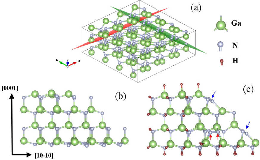
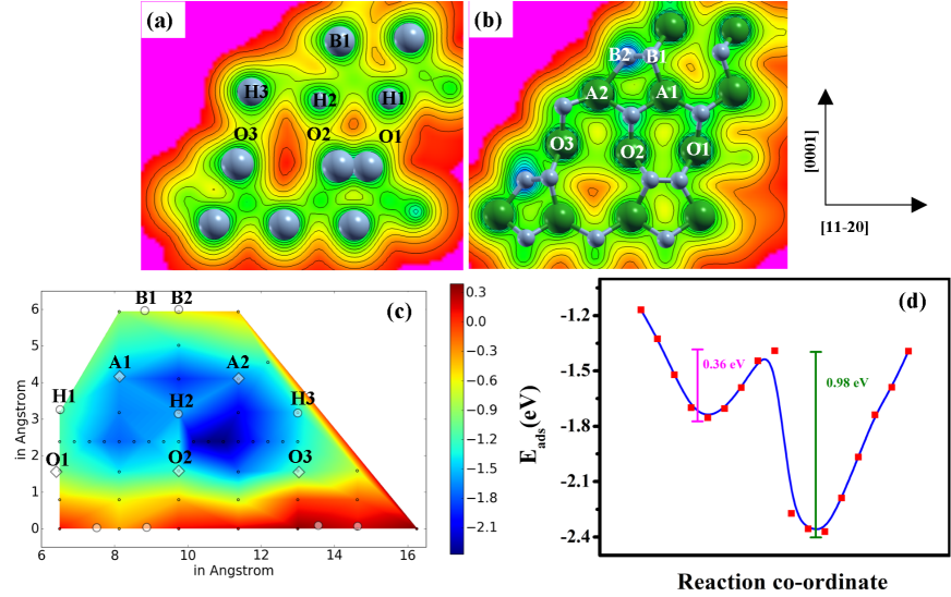
In the relaxed structure of the wedge, we find the Nitrogen (N) having two dangling bonds at surface forms dimers (see Fig.3 (b) and (c)), whereas at the edge a trimer is formed (see blue arrows in Fig.3(c)) due to Stirling’s instabilityLee and Kim (2011). We estimate the adsorption energy of Ga ad-atoms at various positions of the relaxed structure; on the surface and at the edge (see Fig.4(c)). We find that the most favorable sites for Ga adatom are the hollow sites (see Fig.4(c)). The adsorption energy of Ga adatom at the hollow site of O1-O2-A1 triangle is -1.75 eV where the width of the wedge is 6.35 Å whereas, for the hollow site of O2-O3-A2 triangle the adsorption energy is -2.37 eV, while the width is 3.14 Å . We estimate the adsorption energy at various equivalent points on the surface such as at O1, O2 and O3, H1, H2 and H3, as well as at A1 and A2 (see Fig.4 (b) and (c)) and find that the adsorption energy reduces with reduction in the dimension of the wedge. However, interestingly, nearby the N-N dimers and N-N-N trimers, the adsorption energy is substantially high which may be due to the strong bonding character of N atoms. Further, to look at the diffusion barrier of the Ga adatom on the (201) facets, we estimate the adsorption energy at very close distances (0.4 Å) along the [110] direction (see Fig. 4 (d)). It is very clear that, adatoms have to overcome a barrier potential of nearly 0.36 eV to cross from hollow site of O1-O2-A1 triangle to hollow site of O2-O3-A2 triangle, whereas for reverse diffusion the barrier potential is 0.98 eV.
IV Discussion
The nucleation mechanism of GaN on Sapphire has been studied widely in the literatureLukin et al. (2012); Degave et al. (2002); Richards-Babb et al. (1995). Degave et al.Degave et al. (2002) show that growth of GaN on bare surface of Sapphire results in the formation of 3D islands from the early stages of the growth, which is consistent with our observation of the morphology of sample A. It is well known that, in highly lattice mismatched systems (e.g. GaN on c-Sapphire (16%)) the growth mode is governed by the interface and surface energies onlyShchukin and Bimberg (1999). In such systems the strain relaxation of grown island occurs in two different relaxation regimes. At the early stage of growth the elastic relaxation is preferable where the nuclei evolves by aiming to minimize total free energy per unit volume by relieving the lattice mismatch induced strain () and accordingly by reducing their stored elastic strain energy and/or the nuclei attain the lower energy state by changing its shape (such as formation of crystal facets), surface area ()Vanderbilt and Wickham (1990), while with increase in film thickness the plastic relaxation occurs by formation of misfit dislocationsHerman et al. (2013).
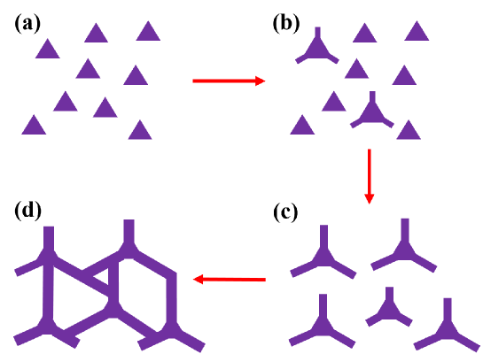
Further, as observed experimentally the wider distribution of island sizes in sample B may be due to the fact that the growth of the dislocated islands is energetically preferable than coherent islands, since the strain energy per unit volume is minimum in the former while later leads to increase in strain energy Krishnamurthy et al. (1991); Drucker (1993), which suggest that the plastic relaxation mechanism took place before 20 minutes growth of the samples . The appearance of pyramidal shaped islands is possible due to the difference in adatoms attachment and/or site exchange rates between atomic steps induced by Ga adlayers on GaN (0001)Fang et al. (2008). The shape transition of such pyramidal islands is mainly governed by the interplay between stored elastic strain energy, total interface and surface energies of all facets composing of all the surfaces of the pyramid. Shchukin et al.Shchukin and Bimberg (1999) pointed out that, edges of the two surfaces could also play a crucial role in the final shape transition, as at this point the discontinuity of the surface stress occurs. Further, Libbrecht et al.Libbrecht (2012) attributed the edge enhanced growth, as seen here, is due to the structure dependent attachment kinetics (SDAK) instability that becomes dominant when diffusion related growth is coupled with structure dependent attachment kinetics of adatoms. Typically, SDAK instability is the consequence of decrease in the nucleation barrier on a faceted surface when the width of the facets decreases, which is consistent from our first-principles calculations. It is relatively easy for Ga ad-atoms to diffuse from thicker part of the wedge to relatively thinner part (towards edge) but the diffusion of ad-atoms from edges of the wedge to the thicker part is energetically not preferable as it has to overcome a large potential barrier of 0.98 eV. Thus, it is evident that a large amount of flow of ad-atoms towards the edges of the pyramid is responsible for edge enhanced growth. This anisotropic growth further sharpens the edge, which enhances the edge growth rate. This positive feedback results in a growth instability which promotes formation of sharp edges. This process continues to lengthen the edges of the tetrahedron until it meets with other similar growing edge of another proximal island to form a junction. Once such junctions are formed, the in-plane growth of the edge stops due to unavailability of thin edges for attachment of the adatoms and the dominant growth will now be along perpendicular direction to the surface of the substrate. Based on the FESEM images and results from first-principles calculations we present a 2D schematics on the morphological evolution and the shape transition of NwN from 3D islands in Fig.5. Further, with increase in the growth time, the side facets of the tetrahedron change from (201) to (100) surface Nayak et al. (2017) due to low surface free energy of the laterDreyer et al. (2014). The final surface morphology observed with higher growth timeThakur et al. (2015); Nayak et al. (2017); Kesaria and Shivaprasad (2011); Thakur and Shivaprasad (2015); Kesaria and Shivaprasad (2011) is consistent with the morphology (hollow columnar) proposed by Libbrecht et al. Libbrecht (2012).
As discussed earlier, the adsorption energy of Ga adatoms nearby the N-N dimers and N-N-N trimers (including at edge) is substantially high, due to the strong bonding character of N atoms. Despite adding an adatom nearby to the dimers they maintain their stability. Such surface and/or edge reconstruction of N atoms are commonly observed in different semipolar surfaces of III-V semiconductors, but their desorption as N2 molecule is energetically favorableLee and Kim (2011); Nishinaga (2014). Thus, the possibility of the presence of dimers and trimers in the grown crystals is negligible.
V Summary
In summary, we have carried out growth of GaN NwN for various durations to monitor the evolution of the surface morphology. At the initial stages we observe the formation of tetrahedron shaped 3D island. With increase in growth time, we observe a wider distribution of islands sizes due to co-existence of coherent and dislocation mediated islands. From first-principles simulations we find that the thinner edges of such tetrahedron are more favorable for attachment of adatoms than their thicker counterparts, resulting in edge driven growth. We find an anisotropy in the diffusion barrier for adatoms on (201) surface depending upon width of the facets, which leads to the formation of the nanowall network. We infer that the evolution from 3D island to NwN morphology is a clear example of SDAK instabilities induced shape transition in thin film growth.
acknowledgement
The authors thank Professor C. N. R. Rao for his support and guidance. SKN acknowledges DST, Govt. of India, for SRF and RK acknowledges UGC, Govt. of India for JRF. All authors acknowledge JNCASR for facilities.
References
- Rastelli et al. (2001) A. Rastelli, M. Kummer, and H. Von Känel, Physical Review Letters 87, 256101 (2001).
- Barth et al. (2005) J. V. Barth, G. Costantini, and K. Kern, Nature 437, 671 (2005).
- Tersoff and Tromp (1993) J. Tersoff and R. Tromp, Physical Review Letters 70, 2782 (1993).
- Brune et al. (1998) H. Brune, M. Giovannini, K. Bromann, and K. Kern, Nature 394, 451 (1998).
- Consonni et al. (2010) V. Consonni, M. Knelangen, L. Geelhaar, A. Trampert, and H. Riechert, Physical Review B 81, 085310 (2010).
- Shchukin and Bimberg (1999) V. A. Shchukin and D. Bimberg, Reviews of Modern Physics 71, 1125 (1999).
- Li et al. (2014) X. Li, C. Wang, and G. Yang, Progress in Materials Science 64, 121 (2014).
- Pimpinelli and Villain (1998) A. Pimpinelli and J. Villain, Physics of crystal growth, Vol. 53 (Cambridge university press Cambridge, 1998).
- Sang et al. (2013) L. Sang, M. Liao, and M. Sumiya, Sensors 13, 10482 (2013).
- Li et al. (2016) G. Li, W. Wang, W. Yang, Y. Lin, H. Wang, Z. Lin, and S. Zhou, Reports on Progress in Physics 79, 056501 (2016).
- Feng (2017) Z. C. Feng, III-Nitride Materials, Devices and Nano-Structures (World Scientific, 2017).
- Himwas (2015) C. Himwas, III-Nitride nanostructures for UV emitters, Ph.D. thesis, Université Grenoble Alpes (2015).
- Kuykendall et al. (2003) T. Kuykendall, P. Pauzauskie, S. Lee, Y. Zhang, J. Goldberger, and P. Yang, Nano Letters 3, 1063 (2003).
- Zhou et al. (2003) S. Zhou, Y. Feng, and L. Zhang, Chemical Physics Letters 369, 610 (2003).
- Colby et al. (2010) R. Colby, Z. Liang, I. H. Wildeson, D. A. Ewoldt, T. D. Sands, R. E. García, and E. A. Stach, Nano letters 10, 1568 (2010).
- Soh et al. (2013) C. Soh, C. Tay, R. J. Tan, A. Vajpeyi, I. Seetoh, K. Ansah-Antwi, and S. Chua, Journal of Physics D: Applied Physics 46, 365102 (2013).
- Yam and Hassan (2007) F. Yam and Z. Hassan, Applied Surface Science 253, 9525 (2007).
- Föll et al. (2006) H. Föll, J. Carstensen, and S. Frey, Journal of Nanomaterials 2006 (2006).
- Wang et al. (2004) Y. Wang, S. Chua, M. Sander, P. Chen, S. Tripathy, and C. Fonstad, Applied Physics Letters 85, 816 (2004).
- Lian et al. (2006) J. Lian, W. Zhou, Q. Wei, L. Wang, L. A. Boatner, and R. C. Ewing, Applied Physics Letters 88, 093112 (2006).
- Thakur et al. (2015) V. Thakur, S. K. Nayak, K. K. Nagaraja, and S. M. Shivaprasad, Electronic Materials Letters 11, 398 (2015).
- Nayak et al. (2017) S. K. Nayak, D. Shamoon, J. Ghatak, and S. M. Shivaprasad, Phys. Status Solidi A 214, 1600300 (2017).
- Kesaria and Shivaprasad (2011) M. Kesaria and S. Shivaprasad, Applied Physics Letters 99, 143105 (2011).
- Thakur and Shivaprasad (2015) V. Thakur and S. Shivaprasad, Applied Surface Science 327, 389 (2015).
- Zhong and Hane (2012) A. Zhong and K. Hane, Nanoscale Research Letters 7, 686 (2012).
- Zhong and Hane (2013) A. Zhong and K. Hane, Japanese Journal of Applied Physics 52, 08JE13 (2013).
- Poppitz et al. (2014) D. Poppitz, A. Lotnyk, J. W. Gerlach, and B. Rauschenbach, Acta Materialia 65, 98 (2014).
- Kushvaha et al. (2017) S. Kushvaha, C. Ramesh, P. Tyagi, A. Shukla, B. Yadav, N. Dilawar, K. Maurya, and M. S. Kumar, Journal of Alloys and Compounds 703, 466 (2017).
- Wu et al. (2009) C. Wu, D. Wuu, P. Lin, T. Chen, and R. Horng, Nanoscale Research Letters 4, 377 (2009).
- Libbrecht (2011) K. G. Libbrecht, arXiv preprint arXiv:1111.2786 (2011).
- Libbrecht (2012) K. G. Libbrecht, arXiv preprint arXiv:1209.4932 (2012).
- Libbrecht (2017) K. G. Libbrecht, Annual Review of Materials Research (2017).
- Soler et al. (2002) J. M. Soler, E. Artacho, J. D. Gale, A. García, J. Junquera, P. Ordejón, and D. Sánchez-Portal, Journal of Physics: Condensed Matter 14, 2745 (2002).
- Perdew et al. (1996) J. P. Perdew, K. Burke, and M. Ernzerhof, Physical Review Letters 77, 3865 (1996).
- Pack and Monkhorst (1977) J. D. Pack and H. J. Monkhorst, Physical Review B 16, 1748 (1977).
- Lee and Kim (2011) W.-J. Lee and Y.-S. Kim, Physical Review B 84, 115318 (2011).
- Lukin et al. (2012) G. Lukin, C. Röder, E. Niederschlag, Y. Shashev, U. Mühle, O. Pätzold, J. Kortus, D. Rafaja, and M. Stelter, Crystal Research and Technology 47, 121 (2012).
- Degave et al. (2002) F. Degave, P. Ruterana, G. Nouet, J. Je, and C. Kim, Materials Science and Engineering: B 93, 177 (2002).
- Richards-Babb et al. (1995) M. Richards-Babb, S. Buczkowski, Z. Yu, and T. Myers, MRS Online Proceedings Library Archive 395 (1995).
- Vanderbilt and Wickham (1990) D. Vanderbilt and L. Wickham, MRS Online Proceedings Library Archive 202 (1990).
- Herman et al. (2013) M. A. Herman, W. Richter, and H. Sitter, Epitaxy: physical principles and technical implementation, Vol. 62 (Springer Science & Business Media, 2013).
- Krishnamurthy et al. (1991) M. Krishnamurthy, J. Drucker, and J. Venables, Journal of Applied Physics 69, 6461 (1991).
- Drucker (1993) J. Drucker, Physical Review B 48, 18203 (1993).
- Fang et al. (2008) Z. Fang, J. Kang, W. Huang, H. Sun, M. Lu, J. Kong, and W. Shen, The Journal of Physical Chemistry C 112, 4925 (2008).
- Dreyer et al. (2014) C. E. Dreyer, A. Janotti, and C. G. Van de Walle, Physical Review B 89, 081305 (2014).
- Nishinaga (2014) T. Nishinaga, Handbook of Crystal Growth: Fundamentals (Elsevier, 2014).