The structure and evolution of semiconducting buffer graphene grown on SiC(0001)
Abstract
Using highly controlled coverages of graphene on SiC(0001), we have studied the structure of the first graphene layer that grows on the SiC interface. This layer, known as the buffer layer, is semiconducting. Using x-ray reflectivity and x-ray standing waves analysis we have performed a comparative study of the buffer layer structure with and without an additional monolayer graphene layer above it. We show that no more than 26% of the buffer carbon is covalently bonded to Si in the SiC interface. We also show that the top SiC bilayer is Si depleted and is the likely the cause of the incommensuration previously observed in this system. When a monolayer graphene layer forms above the buffer, the buffer layer becomes less corrugated with signs of a change in the bonding geometry with the SiC interface. At the same time, the entire SiC interface becomes more disordered, presumably due to entropy associated with the higher growth temperature.
I Introduction
The first graphene “buffer” layer that grows on the SiC(0001) surface is one of the most important examples of functionalized graphene. It is normally in a semiconducting state due to self functionalization caused by sp3 bonding to silicon atoms in the SiC interface.Emtsev et al. (2008); Nevius et al. (2015) The buffer’s bandgap can be increased by additional functionalization with fluorineWalter et al. (2016) or transformed to a metallic graphene form by H2 intercalation that breaks the sp3 bonding to the interface Si.Riedl et al. (2009) In fact numerous studies have shown that the buffer graphene’s electronic properties can be altered by changing the interfacial Si bonds,Mattausch and Pankratov (2007); Varchon et al. (2007); Kim et al. (2008); Varchon et al. (2008); Riedl et al. (2009); Nevius et al. (2015); Walter et al. (2016); Conrad et al. (2017) implying that the buffer’s electronic properties can in principle be modified in a controlled fashion. However, the level of understanding necessary to systematically alter the buffer’s properties has remained illusive because structural details, like the number of C-Si bonds and their geometry, are simply not well understood.
The bonding geometry problem is underscored by the number of different states calculations predict for the buffer. Ab initio calculations using a R30 cell find a wide bandgap buffer while calculations on larger, experimentally observed cellsBommel et al. (1975); Forbeaux et al. (1998) find metallic states running through the Fermi Energy ().Mattausch and Pankratov (2007); Varchon et al. (2007); Kim et al. (2008) The applicability of these early calculations is problematic because they all assumed that the SiC surface is bulk terminated,Kim et al. (2008); Varchon et al. (2008); Sforzini et al. (2015) an assumption that we now know is incorrect. Recent x-ray diffraction studies have demonstrated that the buffer-SiC interface is not commensurate with SiC.Conrad et al. (2017) Instead, the system has an incommensurate (IC) modulation period () that is close to the subcell of the the cell. Tight binding (TB) calculations, using an IC in-plane distortion of a bulk terminated surface, show that the distortion can open a bandgap similar to that measured by angle resolved photoemission (ARPES).Conrad et al. (2017); Nevius et al. (2015) However, before more sophisticated ab initio calculations on the IC structure can be attempted, some details of the interface structure will be needed to limit the parameter space for these taxing computations.
Experimentally determining the buffer’s structure is also problematic. The first experimental structural studies were done on samples grown in ultra high vacuum (UHV).Hass et al. (2008) These samples suffered from both reduced long range orderCharrier et al. (2002); Hass et al. (2006); Gao et al. (2008) and poor control of both the number of graphene layers and their lateral distribution.Charrier et al. (2002); Riedl et al. (2007) Sample uniformity turns out to be extremely important because both the buffer’s electronic and structural properties are now known to change when monolayer (ML) graphene grows above the buffer.Conrad et al. (2017) This means that measured structures on nonuniform films represent some unknown average of two different structures.
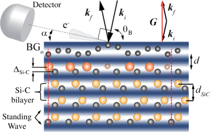
In this work, we use x-ray standing wave (XSW) and x-ray reflectivity (XRR) measurements to study two types of buffer graphene films grown on SiC(0001): a buffer-only film (BGo) and a buffer graphene film (BGML) that has a monolayer graphene layer grown above it. Because of the improved thickness control and the layer uniformity achievable in silicon sublimation controlled RF furnace grown graphene, we are able to discriminate structural changes in these two different types of buffer graphene. We show that the buffer structure and the bonding to the SiC are very different with and without a monolayer graphene layer grown above the buffer layer. While these differences help explain recent in-plane x-ray diffraction results,Conrad et al. (2017) they complicated previous XSW analysis that used multilayer films and led to a misidentification of the buffer-SiC bonding component in the buffer’s C1s spectrum.Emery et al. (2013) We also show that the buffer-only film has a large vertical corrugation and that its close distance to the substrate indicates a strong sp3 C-Si bond. The buffer’s C-Si bond length increases and the corrugation amplitude becomes smaller when the ML grows above the buffer, indicating a change in the distribution of graphene-Si bonds to the SiC interface. Finally, we confirm that the Si concentration in the last Si-C bilayer [see Fig. 1] is reduced as previously reported.Emery et al. (2013) Rather than being a growth artifact as perviously conjectured, we show that Si vacancy concentration is an equilibrium structure of the top SiC bilayer. We find 25% SiC vacancies in the top SiC bilayer (compared to the bulk value) for both BGo and BGML films. This result helps put an upper limit of 26% on the number of buffer-carbon atoms bonded to silicon at the interface. The reduced Si concentration is coupled with a vertical compression in the Si-C bilayer below the buffer, suggesting that the Si vacancy concentration may help drive the incommensurate structure of the BGo and SiC interface.
II Experimental Methods
II.1 Sample Preparation
The substrates used in these studies were n-doped CMP polished on-axis 4H-SiC(0001). The graphene was grown in a confinement controlled silicon sublimation furnace (CCS).de Heer et al. (2011) In the CCS method, graphene growth is a function of temperature, time, and crucible geometry that sets the silicon vapor pressure. With the current crucible design,Nevius (2016) a single semiconducting BGo graphene layer grows at a temperature of 1400after 30 min. Heating at 1560for 20 min causes the BGo layer to transform into a graphene ML as a new BGML buffer layer forms below the ML. Prior to XSW and XRR experiments, the BGo and BGML+ML samples were characterized by x-ray photoemission spectroscopy (XPS) and Raman to determine film quality and ML coverage.
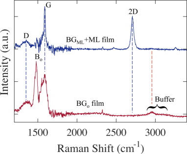
Figure 2 compares the Raman spectra of the BGo film to the spectra from a BGML+ML film. The BGo film spectrum lacks the ML 2D and sharp G peaks but shows two additional features; a Bo peak at 1480 cm-1 and a broad G+D peak between 2900-3100 cm-1. The latter two features are known to be associated with a pure buffer film.Fromm et al. (2013); Palmer et al. (2014) Using the ML 2D intensity as a reference and the background noise as an upper limit on the buffer 2D peak, we estimate that the ML coverage must be less than . This is consistent with ARPES estimates of the ML coverage in a BGo film.Nevius et al. (2015) The majority of the ML coverage is expected to be associated with ML that nucleates at intrinsic step edges.Emtsev et al. (2009) The Raman spectrum was measured at three positions (each 3 mm apart) on the sample and no significant changes in the Raman were found, indicating the large scale film uniformity necessary for XRR experiments.
II.2 XSW and XRR Methods
XRR measurements were conducted at room temperature in UHV at the SIXS beamline at the Synchrotron SOLEIL using a photon energy of keV. Prior to X-ray exposure, the samples were heated to 500in UHV to remove absorbed contaminants. The momentum transfer vector, , is defined as where and are the momenta of the incident and reflected x-ray beams, respectively, For elastic scattering considered here, . represents a point in reciprocal space that is written in terms of the bulk hexagonal coordinates of SiC: where and . The XRR polarization and geometric corrections were performed to allow comparison between the measured reflectivity intensities and calculated intensities from the model discussed in Sec. III.3.Vlieg (1997)
In the XSW experiment, the sample is oriented so that the incoming x-ray beam of energy satisfies the condition that , where is a reciprocal lattice vector of SiC (i.e., a Bragg reflection). This geometry produces a standing wave whose crests are apart and perpendicular to [see Fig. 1]. By changing the incident photon energy relative to , the standing wave will move in the -direction exciting photoelectrons as a wave maxima passes through a plane of atoms [see Fig. 1].Zegenhagen (1993); Bedzyk (2005) The photoelectron intensity for a particular element in the material, , will therefore be a function of and thus related to the vertical position of that element.
The XSW experiments were carried out at the GALAXIES beamline on the Synchrotron SOLEIL.Rueff et al. (2015) We used the Bragg reflection to produce the standing wave with Å. The Bragg angle for the (004) reflection was corresponds to an incident photon energy of eV. All measurements were done at room temperature with an overall energy resolution better than 250 meV. The take-of-angle, , for the photoelectron detector was to improve surface sensitivity in the XPS spectra.
For the studies presented in this work, we are interested in the photoelectron yield from the C1s core levels that have components from both the carbon in SiC and the carbon in the buffer layer. The details of analyzing the C1s spectra as a function of both photon energy and binding energy require some care. We do this by first setting the number of components in the spectrum [see Sec. III.1] and then fitting each spectrum for a range of photon energies around . The fitting is done by minimizing the global [see supplemental material]. The global is the for a single C1s spectrum fit, at a single photon energy, summed over fits for every incident photon energy in the data set. While each component’s line shape parameters, i.e., width and position, are allowed to vary, they are constrained to be independent of the incident photon energy. Only the components’ areas are allowed to vary as a function of . A Shirley background has been subtracted from every core-level spectrum. We use a Doniach-Sunjic lineshape for the graphene peak and a Voigt lineshape for the buffer carbon, bulk carbon component, and Si 2s core-levels.
III Results
While XRR is able to study surfaces with buried interfaces, the phase problem makes structural measurements difficult. Emery et al.Emery et al. (2013) have shown how combining XSW and XRR studies of the SiC-graphene interface can help overcome the phase problem. However, in the particular case of the buffer layer, XSW analysis has its own problems that were not recognized and that we now discuss before presenting our experimental results.
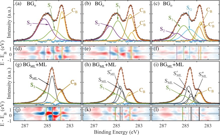
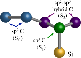
The C1s XPS spectra of graphene grown on SiC(0001) was thought to contain four components; S1, S2, SML, and CB. S1 and S2 are from the buffer carbon layer that contains C-Si bonds to the interface and distorted C bonds in the unbonded part of the buffer layer. The SML component is from sp2 C-C bonds in any graphene that grows above the buffer. The CB component is from sp3 C-Si bonds in bulk SiC.Emtsev et al. (2008) However, several theoretical calculations along with experimental scanning transmission electron microscopy (STEM) and x-ray diffraction measurements show an incommensurate structure that suggests reduced interfacial bonding. All these works indicate that part of the buffer should also have sp2 bonded carbon.Kim et al. (2008); Conrad et al. (2017); N. Nair et al. (2017) This possibility is shown schematically in Fig. 3 and implies at least one additional component (we label SG) may be present in the buffer’s C1s spectrum. Any partial ML film would have an SML component obscuring any possible sp2 bonded carbon in the buffer layer’s C1s spectrum. Furthermore, any substantial reconstruction of the the top SiC bilayer could also cause new components to arise in the C1s spectrum near the BE of the bulk CB component. It will therefore be important in our subsequent XPS analysis to explore how additional C1s peaks affect the XSW results.
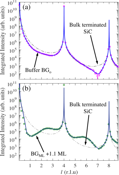
The large ML coverages in samples used in earlier studies cause an additional and more important problem. If the BGo and BGML layers were structurally identical, the ML coverage would only complicate the spectral analysis of the C1s spectrum. We now know that this assumption is wrong and that there are substantial changes in the buffer’s structure when a ML grows above it.Conrad et al. (2017) This means that a substantial ML coverage will cause both the XSW and XRR data to give results that represent an unknown weighted average of two different structures making it impossible to determine a unique BGo structure. For XRR, the ML coverage has a further complication. Because both the BGo and BGML layer distributions are broad in while ML or bilayer graphene layers are narrow,Emery et al. (2013); Sforzini et al. (2015) the buffer’s contribution to the scattered amplitude will be smaller than the ML’s.Robinson and Vlieg (1992) This effect is demonstrated by comparing the calculated XRR reflectivity of a bulk terminated SiC surface to the measured buffer or ML films [see Fig. 4]. Between Bragg peaks (= 0,4, and 8), the buffer layer causes small changes (about a factor of 4-10) with respect to the bulk terminated surface. A ML film on the other hand can produce changes that are a factor of 10 larger and thus obscure reflectivity contributions from the buffer film [see Fig. 4(b)].
The problems associated with ML films we identified above are the reasons we use samples with high coverage control. Our XSW studies will consider the possibility of new components in the C1s fits. Recognizing the possible systematic errors associated with multiple peak fits in the C1s spectra, we will use the XSW derived -distributions as starting parameters for XRR reflectivity fits. These distributions will be allowed to vary (with restrictions) to refine the BGo and BGML layers structure.
III.1 Fitting the XPS Spectra
Figure 5(a) shows a 3-component fit (S1, S2, and CB used in previous studies) to the BGo layer when no ML graphene is expected on the sample. It must be emphasized that the relative areas of the individual components in Fig. 5 are not a measure of their relative concentrations as will be discussed in Sec. III.2. In fact the photon energy used for the C1s spectra shown in Fig. 5 was deliberately chosen to minimize the S1 component that can obscure any components that occur in an energy range where a graphene ML component would appear. Our 3-component fit is very similar to those found in the work of Emtsev et al.Emtsev et al. (2008). In that earlier work, the C1s spectrum was monitored as a function of growth, so we would expect very little ML coverage in their early growth spectra, explaining the similarity of their fit to ours.
While 3-components can fit the C1s spectrum, there are large residuals [see Fig. 5(d)] suggesting that other peaks could be present. As discussed above and shown in Fig. 3, we expect the BGo layer to have a structure that could have an additional C1s component. However, if we add a 4th component near the BE of ML graphene (285.5 eV), the fitting procedure moves the peak to a position close to the bulk CB position. Because of its proximity to CB, we label the new peak C’B [see Fig. 5(b)]. It is certainly reasonable that the top SiC bilayer would relax as some bilayer Si bonds to the buffer and distorts the bilayer Si-C bonds. This would strain the top SiC bilayer from the bulk configuration and lead to a range of binding geometries that would broaden the CB peak and possible give rise to a C’B component. The overall effect on the C1s fit using the C’B component is very dramatic. The intensity ratio of S1 to S2 reverses and both peaks become narrower as S1 moves to higher BE. Note that despite these changes, the residual map is only slightly improved [see Figs. 5(e)].
The residual map for the BGo film can be substantially improved by adding a 5th component [see Figs. 5(c) and (f)]. The best fit position of the new peak is labeled SG because its BE is near that of graphite, between the BE of the buffer peaks and the bulk carbon peaks. The SG peak causes S1 to move to even higher BE and further increase the intensity ratio of S1 to S2. In fact, the spectral ratio of S1 to S2 in the 5-component fits resembles that found by Emery et al.,[Emery et al., 2013] using a ML film. The similarity between our 5-component fit and Emery et al.,[Emery et al., 2013] might be expected given that the SG peak influences the fit shape in much the same way as a true ML graphene peak would. The peak positions and widths of the different component fits for the BGo C1s spectra are summarized in Table 1. As we’ll show in Sec. III.2, the three different C1s decompositions lead to very different BGo layer structures.
| FW | FW | FW | |||||
| Buffer | 3-Comp | 1.58 | 1.38 | 0.74 | 1.38 | - | - |
| 4-Comp | 1.92 | 1.15 | 1.23 | 1.07 | - | - | |
| 5-Comp | 2.12 | 1.12 | 1.51 | 1.21 | 0.99 | 1.37 | |
| FW | FW | ||||||
| ML | 3-Comp | - | - | 1.35 | 1.37 | 0.77 | 0.57 |
There are also multiple ways to fit the ML film’s C1s spectra. Figures 4(g-i) show fits for a BGML+ML film using different numbers of C1s components. The 3-component fit [Figs. 4(g)] gives a reasonable fit to the ML C1s spectrum. Note that we label the higher binding energy peak as S1 not S2. This is because its BE lies closer to S1 in the BGo 4- and 5-component fits. As we’ll show in Sec. III.2, the assignment of the highest BE peak to S1 will be supported by the XSW results. Adding other components significantly improve the residuals [see Figs. 4(j), (k), and (l)] but has remarkably little affect on the parameters for the S1 component. We label these additional peaks and because no matter the starting position, their best fit BE cluster around the SML monolayer peak’s BE. While adding and improves the fits, they are too weak and too close together to get reliable yield curves for subsequent XSW analysis [see supplemental material]. This is in part due to attenuation effects of the BGML components by the ML film above. We will therefore only report on the S1 and SML parameters for the 3-component fits parameters [see Table 1] and wait until the XRR data is presented to give a better estimate of the BGML structure.
III.2 X-ray Standing Waves
The normalized photoelectron yield for element in an XSW experiment is given by:Zegenhagen (1993); Bedzyk (2005)
| (1) | ||||
is the energy dependent x-ray reflectivity at the Bragg point ( in this work) and is the phase of the standing wave [see supplemental material].Zegenhagen (1993) Both are calculated from the bulk crystal structure.Authier (2001) is the density distribution of the element and [where is the position of the jth atom, modulo ]. Rather than deal with arbitrary atom distributions, we will only consider atoms vertically distributed in discrete planes at positions in a Gaussian distribution. This is done by writing as a convolution of a delta function with a normalized gaussian distribution whose width is . This reduces Eq. 1 to:
| (2a) | ||||
| (2b) | ||||
is related to the experimental intensity by a normalizing constant; . Neglecting photoelectron attenuation (a reasonable assumption for the buffer only film) the coverage of a given C1s component is then related to the ’s;
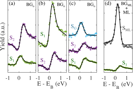
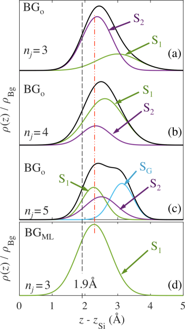
Figures 6(a), (b), and (c) show the experimental yields for the BGo film derived from 3-,4-, and 5-component C1s fits. The fit for the ML film, using 3 C1s components, is shown in Fig. 6(d). All fit parameters are summarized in Tables 2 and 3. While all the BGo fits are very good, regardless of the number of components in the spectral decomposition, there are major differences in their -distributions. To make comparisons between the different fits easier to visualize, we have plotted their different -distributions in Fig. 7. For reference, we have marked the 1.9Å C-Si bond distance between buffer carbon and interfacial silcon measured by STEM in Fig. 7.N. Nair et al. (2017) Note that the STEM value is close to the 1.89Å bulk SiC bond length.
There are a number of observations from the XSW results that indicate that the 5-component fit is closer to the actual BGodistribution. First, the 3- and 4-component fits give a BGo distribution that is essentially a broad Gaussian with the S2 component closer to the SiC interface [Figs. 7(a) and (b)]. The essentially Gaussian shape is inconsistant with experimental STEM profiles of the buffer that indicate a sharper -distribution.N. Nair et al. (2017) In fact the 3-component fit finds that the S2 atoms closer to the SiC are more than twice as numerous than the S1 atoms farther away [see Table 2]. This contradicts both STEM results and theory predictions that the bonded carbon (presumably S2 in the 3- and 4-component fit) is a much smaller fraction of the buffer carbon. Finally, both the 3- and 4-component fits find the unphysical result that 23% of the buffer carbon lies closer to Si than the smallest known C-Si bond distance of 1.89Å.
| 111The position of the Si layer is determined by the XSW yield fits to the Si 2s core level; Å [see Table 3]. | ||||||
| (Å) | (Å) | |||||
| BGo | S2 | -0.02(2) | 2.37(4) | 0.52(4) | 0.46(2) | 0.70(1) |
| (3-peak) | S1 | 0.23(5) | 3.01(1) | 0.3(4) | 0.6(1) | 0.30(1) |
| BGo | S2 | -0.04(1) | 2.33(4) | 0.56(5) | 0.43(3) | 0.24(1) |
| (4-peak) | S1 | 0.07(3) | 2.61(7) | 0.36(4) | 0.58(3) | 0.76(2) |
| BGo | S2 | -0.03(5) | 2.5(1) | 0.48(9) | 0.48(7) | 0.32(1) |
| (5-peak) | S1 | -0.07(1) | 2.26(3) | 0.67(5) | 0.36(4) | 0.31(1) |
| SG | 0.28(2) | 3.13(6) | 0.7(2) | 0.3(1) | 0.36(2) | |
| BGML | S1 | -0.06(2) | 2.30(5) | 0.41(2) | 0.52(3) | - |
| ML | 0.27(2) | 5.63(5) | 1.0(1) | 0.0(1) | - |
| (Å) | (Å) | ||||
| BGo | CB | -0.24(1) | 1.92(2) | 0.79(5) | 0.27(4) |
| SiB | 0.04(1) | 0.09(2) | 1.00(3) | 0.05(4) | |
| BGML | CB | -0.25(1) | 1.89(2) | 0.72(5) | 0.33(2) |
| SiB | 0.04(1) | 0.09(2) | 0.99(3) | 0.07(4) |
There is one more result that points to the 5-component C1s fit being the correct deconvolution of the BGo XPS spectrum. As already noted, XSW analysis predicts that the S2 component from 3- and 4-component fits to the C1s XPS spectra fits is associated with buffer carbon closest to the last bulk Si layer. This was the same result found in XSW experiments by Emery et al.Emery et al. (2013) using a ML sample. However, our 5-component XSW analysis shows just the opposite result. Using the 5-component fit, we find that S1 is closest to the Si layer indicating that S1, not S2, is from buffer carbon bonded to silicon. The proposal that S1 is closest to the Si layer was first made by Emtsev et al.Emtsev et al. (2008) in XPS studies on a series of samples ranging from no graphene to several monolayers. They noted that the buffer’s -bands were downshift by 1.0 eV compared to graphite. The shift meant that the S1 and S2 buffer carbon peaks were also shifted to high BE relative to neutral graphite. Since the sp2 bonded carbon must be at a higher BE than C-Si bonds, they concluded that the S1 feature must be associated with buffer-Si bonds. The Emtsev interpretation that S1 is closer to the SiC is further supported by comparing our ML and buffer layer results. We only need 3-components to fit the BGML+ML film’s C1s spectra: the ML SML peak, the bulk CB peak, and a component from the BGML layer. The BGMLcomponent was labeled as S1 in Fig. 5. Since the BGML S1 component is the only component close to the interface in the ML film, it must have a considerable fraction of carbon bonded to Si. In other words, the BE of S1 in the ML film should be similar to the BE of the component in the BGo layer that is bonded to Si in the interface. At the same time, the components that binds to Si in both the BGo and BGML must be approximately the same -distance from the top Si layer. A comparison of the BGo and BGML+ML film data in Table 1 and the red dashed line in Fig. 7 shows that only the S1 peak in the 5-component C1s spectrum meets both these combined requirements. Based on these observations, we propose that the 5-component fit to the BGo layer’s XPS data represents the actual C1s spectra and that the previous Emtsev et al.Emtsev et al. (2008) interpretation correctly assigns S1 as being the BGo carbon component bonded to Si. The incorrect assignment of the bonding species in the prior XSW analysis was most likely due to the XPS signal being a mixture of of two different spectra from ML and buffer layer partial coverages.
The XSW derived distance between the S1 carbon in the BGo layer and the top Si layer is 2.26Å, comparable to the 2.1(1)Å distance measured in previous XSW workEmery et al. (2013) but is larger that the 1.9Å bond length measured by STEM.N. Nair et al. (2017) The differences between the XSW results and STEM values is likely due to assigning the Si top layer -position as the zero of the -scale based solely on the value derived from the Si 2s XSW yield. Since the Si 2s yield contains contributions from several bilayers, which we will show have different -distributions, the XSW derived Si position will have systematic errors.
Finally, even though the 5-component gives the best overall density profile, their are problems. The density profile is not as sharp as sharp as STEM results would have predicted. Furthermore, we expect from the model in Fig. III that there should be significantly more S2 carbon compared to S1. The XSW results in Table 2 give nearly the same concentrations for both S1 and S2. We believe these problems with the XSW results are associated with the difficulty of accurately deconvoluting the closely spaced C1s components in the XPS spectra. To improve on the XSW structural result we must combine these findings with our XRR results of the BGo and BGML+ML films.
III.3 Surface X-ray Diffraction
To fit the x-ray data, we use four SiC bilayers above the bulk with a buffer graphene layer above [see Fig. 1. We also allow up to two partial graphene layers above the buffer. The scattered x-ray intensity is then:
| (3) | ||||
where is the bulk 4H-SiC structure factor,Bauer et al. (2001) modified by the crystal truncation term, [see Ref. Robinson, 1986], is the structure factor of the 4-bilayer SiC interface region , is the buffer graphene structure factor, and is the structure factor of any ML graphene layers above the buffer. and in Eq. (3) are weighted by the ratio of the areal atomic densities of a 4H-SiC and a graphene (0001) plane; =3.132. The factor properly normalizes the scattered amplitude from the graphene layer per 4H-SiC unit cell. is a term that contains all corrections due to the experimental geometry.Robinson (1991); Vlieg (1997); Feng (2006) The exponential term accounts for the substrate roughness caused by half-cell step fluctuations in the SiC surface (the predominant step height on 4H samples;Hass et al. (2006) ). is the variance in the number of half-cell layers in the surface due to steps.Elliott et al. (1996) Roughly, is proportional to the SiC step density.
in Eq. (3) is the structure factor of the top four SiC C-Si bilayers plus an additional layer of Si to allow for the possibility of Si adatoms or a relaxed Si layer bonded to the buffer graphene [see Fig. 1]. The interface structure factor is then:
| (4) |
where is the relative atom density for the interface layer at a vertical position ( for a bulk layer corresponding to ). It was found that the additional Si layer was not needed to fit the experimental reflectivity and will not be discussed in Sec. IV. The zero height is chosen as the top layer of Si atoms in the top SiC bilayer. is the atomic form factor of C or Si depending on the layer. A normalized Gaussian of width has been convoluted with each layer to included possible layer disorder (similar to Eq. 2b used to describe the XSW vertical distribution).
To be consistent with the XSW results, we allow the buffer to be composed of distinct carbon layers. The multilayer graphene structure factor can then be written in a general form similar to Eq. 4:
| (5) |
where is the atomic form factor for carbon, is the areal coverage of buffer graphene, and is the fractional coverage of each component in the buffer such that . The structure factor of graphene above the buffer layer is:
| (6) |
where is the coverage of the mth graphene layer.
To fit the experimental reflectivity to Eq. 3, we use a lasso fitting routine.Tibshirani (1996) The lasso technique allows us to use the XSW derived buffer and known SiC bulk parameters as starting points (default parameters). Changes in these parameters are penalized in the ordinary least squares regression (OLS). The penalties are initially set to be very large to identify which parameters in Eq. 3 give the largest reduction in the OLS . Gradually, all penalties are reduced and new default parameters are updated until the model has converged to the minimized [see supplemental material].Conrad (2017) This enables a seamless connection of the XSW derived parameters with the XRR parameters, placing the results of both techniques on an equal footing.
| -(Å) | (Å) | (MLG) | Interface layer | ||||||||||
|---|---|---|---|---|---|---|---|---|---|---|---|---|---|
| (MLSiC) | |||||||||||||
| S1 | S2 | SG | S1 | S2 | SG | S1 | S2 | SG | (Å) | Si | C | ||
| BGo | XRR | 1.9(1) | 2.7(1) | 3.8(1) | 0.15(5) | 0.27(2) | 0.3(1) | 0.26(6) | 0.47(6) | 0.26(4) | 0.47(2) | 0.75(10) | 0.9(2) |
| XSW | 2.26(3) | 2.5(1) | 3.13(6) | 0.36(4) | 0.48(7) | 0.3(1) | 0.33(1) | 0.32(1) | 0.36(2) | 0.69(2) | - | - | |
| BGML | XRR | 2.22(7) | - | - | 0.2(1) | - | - | 0.9(1) | - | - | 0.46(5) | 0.79(5) | 0.8(1) |
| XSW | 2.30(5) | - | - | 0.52(3) | - | - | - | - | - | 0.33(2) | - | ||
IV Discussion
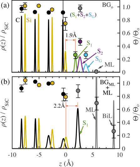
Figure 8 shows a comparison of the density profiles from the buffer BGo and BGML+ML films derived from the XRR fits in Fig. 4. The fit parameters are given in Table 4. The calculated reflectivity for a buffer BGo film starts with the S1, S2, and SG positions and widths derived from the XSW parameters. Fits starting with only S1 and S2 always have an order of magnitude higher values and will not be discussed here.Conrad (2017) The higher values, using only two carbon layers in the buffer, supports our early argument that a 5-component fit to the C1s spectrum is necessary to get the correct vertical position of S1 and S2 from the XSW analysis. The ML film uses a single component for the BGML film as determined from the preceding XSW analysis. Note that the XRR determined ML coverage is less than 1% for the BGo film [see Fig. 8(a)], consistent with the Raman ML estimate in Fig. 2.
Like the XSW profiles, the XRR analysis shows that the BGo layer distribution is very broad compared to the BGML layer in the ML film. Associated with the change in the buffer’s -width, we find that the buffer-Si distance gets larger by 0.3Å when a ML has grown above it. This vertical change in distance results in a physically reasonable volume conservation when one also considers the previously observed transition from the larger in-plane incommensurate lattice spacing of BGo to the smaller commensurate lattice in the case of BGML.Conrad et al. (2017) It apparently occurs concomitantly with a change in the distribution of buffer-Si bonds at the interface. Both the change in width and bond distance are consistent with ARPES measurements that show a change in the band structure of the buffer when a ML grows above it.Conrad et al. (2017)
The XRR analysis finds that the bonding component S1 in the BGo layer is 1.9Å above the top Si layer; the same distance measured by STEM.N. Nair et al. (2017) The distance between the buffer S1 carbon and the last Si layer is essentially the same as the bulk Si-C bond (1.89Å) confirming that the bond between S1 carbon and substrate Si has a significant covalent component.Emery et al. (2013); N. Nair et al. (2017) We note that the XRR derived distance for S1 is about 17% closer to the interface than the XSW result. As discussed in Sec. III.2 this small difference is not unusual given that the top Si-layer position is determined from the XSW yield of the Si 2s spectrum that has a significant contribution from deeper bulk-like bilayers with different vertical laxations. Indeed, while the XSW analysis give the C-Si separation in the top SiC bilayer to be 0.69Å, nearly the bulk value (0.63Å), the XRR analysis finds that the C-Si separation has relaxed to be nearly 30% shorter (0.47Å) than in the bulk [see Table 4].
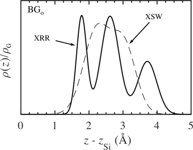
The XRR derived vertical density profile of the BGo layer is both sharper and wider than the XSW distribution. Figure 9 shows a comparison of the XRR and XSW derived distributions. The change in the sharpness of the BGo distribution is due to a narrowing of the XRR derived S1 width compared to the XSW results [see Table 4]). The XRR determined BGo layer width is Å compared to Å (including s) found in the XSW analysis. We point out that both our XRR and XSW BGo widths are much wider than the previous XSW results of Emery et al.Emery et al. (2013) (FWHM=0.9Å). The difference is not unexpected because the prior XSW results were from multi-layer graphene films with a large areal coverage of BGML buffer and a much smaller coverage of BGo buffer. Based on our ML results, the early UHV films, which were composed of primarily ML graphene with little BGobuffer,Emery et al. (2013) would have measured a buffer width that was a weighted average of a majority BGML film with width Å and a minority contribution from the broad BGo film with width Å. Assuming a 80% ML film, an average buffer width of 0.8Å would have been measured; close to the 0.9Å that was measured in Ref. [Emery et al., 2013].
While we find a wide BGo layer, it is not unprecedented. Large vertical buffer layer widths have also been suggested by scanning tunneling microscopy (STM) measurements. Chen et al.,Chen et al. (2005) argue that large amplitude height variations in the buffer structure, seen in both filled and empty state images, are topographical. They find vertical oscillations between 1.5Å and 3.2Å. The larger widths were observed in films that were annealed for longer times, implying that they are associated with more ordered buffer films. However, similar oscillations seen by Riedl et al.,Riedl et al. (2007) were interpreted as being partially due to electronic effects so it remains difficult to make comparisons of our BGo layer width with STM measured corrugations. Ab initio calculations, using a bulk terminated SiC surface, predict a significant BGo layer modulations of 1.2Å.Varchon et al. (2008) As we now discuss, the interface is far from bulk terminated and could induce much larger theoretical modulations if a more realistic SiC interface structure was used.
The structure of the SiC interface layer and how Si in this layer is bonded to buffer carbon are the most important questions about this system. The reflectivity shows that while the last Si layer remains relatively sharp, its density is only 75% of its bulk value (i.e., 20% Si vacancies) [see Table 4]. A similar Si vacancy concentration was reported in previous XRR studies using UHV grown samples and was presumed to be due to a growth artifact.Emery et al. (2013) Our results strongly suggest that the depleted top Si layer is in fact an equilibrium structure. We say this because the depleted fraction in the top Si layer is independent of the growth method. The Si vacancy concentration in our high temperature, high Si vapor pressure environment is the same as the concentration found in the prior low temperature, low Si vapor pressure UHV environment.Emery et al. (2013) Furthermore, the Si vacancy concentration is the same in both the BGo and BGML+ML films [see Table 4] even though the ML grows at a temperature 150higher than the BGo layer. All of these results point to the depleted top Si layer being an equilibrium structure that is relatively independent of temperature and Si vapor pressure. The idea that Si vacancies may exist in the buffer-SiC system has been explored theoretically. Calculations have shown that Si vacancies or C interstitial in the interface layer below the BGo layer lead to lower total surface energies that can give rise to a number of possible large BGo corrugations.Kageshima et al. (2011)
Besides the high Si vacancy concentration, there is a significant change in the carbon-silicon spacing in the top SiC bilayer. The C-Si -spacing, , in the SiC bilayer below BGo is 30% shorter compared to a bulk SiC bilayer and half the distance predicted by ab initio calculations in a bulk terminated surface with a BGML+ML film.Sforzini et al. (2015) It is likely that the vacancies in the top SiC bilayer lead to the additional bulk peak in the 5-component C1s spectra in Figs. 5(b) and (d). We suggest that not only are Si vacancies a part of the equilibrium SiC-buffer system but that they most likely drive the incommensurate buffer-SiC structure recently found in surface x-ray diffraction studies.Conrad et al. (2017) We expect that future theoretical work will support this assertion.
We point out that while the XSW analysis finds that there is equal S2 and S1 carbon [see Table 4], the XRR derived coverages find that there are nearly twice as many S2 carbon atoms compared to S1. The higher S2 coverage is more constant with the model in Fig. 3 that would suggest approximately a 3:1 ratio of S2 to S1. Since the S1 bonding component, derived from the XRR, makes up 26% of the carbon in the BGo layer [see Table 4], the S1 coverage must put an upper limit on the number of Si-graphene bonds in the buffer layer. If each S1 carbon atom bonds with a single Si atom in the top SiC interface layer, the reflectivity would estimate that 81% of the interfacial Si is bonded to the buffer layer. Of course it is not only the number of bonds that determine the BGo’s electronic structure, but how these bonds are distributed. Ab intio calculations of the BGo layer find that 25% of the buffer carbon is bonded to 78% of the Si in the top layer assuming a bulk terminated surface.Kim et al. (2008) Tight binding calculations using an incommensurate distortion of the bulk surface predict a much lower number of bonded buffer carbon (15%).Conrad et al. (2017) It is very likely that allowing Si vacancies in the top SiC layer will lead to an opening of a gap in the band structure of buffer graphene in ab initio models.
Finally, a comparison of Figs. 8(a) and (b) reveals that, with the exception of the last Si layer, the widths of the interface C and Si remain relatively well ordered after the buffer has formed (Å and Å). Once the ML is grown at a higher temperature, there is considerably more vertical disorder in the interface. In the last two SiC bilayers, the C widths doubles compared to the buffer-only interface and the Si width in the second bilayer triples. The increased vertical disorder is consistent with an increase in the in-plane disorder of the interface and an increase in the BGML in-plane strain when the ML grows.Conrad et al. (2017) Since the ML is grown 150higher than the buffer only film, entropic disorder in the SiC below the ML film may become important. This suggest that annealing studies (at temperatures less than the ML growth temperature) will need to be carried out to see if the interface order can be further improved.
V Conclusion
In this work, we have studied the structure of the first graphene layer that grows on SiC(0001) (known as “buffer” graphene). By using samples with highly uniform and controlled graphene coverages, we are able to show that the buffer’s structure is dramatically altered when monolayer graphene is grown above it. These results correlate well with electronic changes that occur with ML growth. From essentially ML free samples, we are able to clear up inconsistencies in early works as to which component in the buffer’s C1s spectrum is associated with carbon bonded to Si in the SiC interface. We show that the S1 peak at a binding energy of 285.2 eV is from buffer carbon bonded to Si.
One of the most important findings of this work is that the SiC interface below the buffer graphene cannot be bulk terminated. Instead we show that the last Si layer in the SiC interface is substantially reconstructed. By comparing samples grown under different growth conditions, we show that the top Si bi-layer in the interface has a large equilibrium concentration of Si vacancies (20% of the bulk value). The effect of the reduced number of Si atoms is to decrease the top SiC bilayer distance by 30% of the bulk value. This planarization of the SiC bilayer may explain why the SiC interfacial layer, along with the buffer layer, becomes incommensurate with the bulk SiC. We also find that less than 26% of the BGo buffer layer carbon is bonded to the substrate. While the exact density of Si in the top layer cannot be determined, we can report that the number of Si atoms bonded to the buffer carbon can be no more than 55% of the Si atoms in the top SiC bilayer. We believe these results will act as a new starting SiC interfacial structures for future ab initio calculations that will help understand the semiconducting properties of this graphene film.
We also show that the vertical corrugation of the buffer layer is very large, Å and that the buffer’s width reduces to Å when a monolayer grows above the buffer. The reduction in the buffer’s width is associated with a slight increase in the Si-buffer carbon bond length. Finally, we find that the SiC interface becomes more vertically disordered when the monolayer forms. This correlates with previous x-ray diffraction results that find an increase in the buffer’s in-plane disorder when a monolayer forms above it.Conrad et al. (2017) This is most likely due entropic disorder at the higher growth temperature of the monolayer and the decrease of Si out-diffusion caused by the buffer carbon film. The results suggest that annealing may improve the interface order.
Acknowledgments This research was supported by the National Science Foundation under Grant No. DMR-1401193. P.F. Miceli also acknowledges support from the NSF under grant No DGE-1069091. Additional support came from the Partner University Fund from the French Embassy. The authors would like to thank W. de Heer for use of the Keck Lab facilities. Finally, we wish to thank the staff and technical support given for this project by the Synchrotron Soleil under project No’s 20150681 and 20150682.
References
- Emtsev et al. (2008) K. V. Emtsev, F. Speck, T. Seyller, L. Ley, and J. D. Riley, Phys. Rev. B 77, 155303 (2008).
- Nevius et al. (2015) M. S. Nevius, M. Conrad, F. Wang, A. Celis, M. N. Nair, A. Taleb-Ibrahimi, A. Tejeda, and E. H. Conrad, Phys. Rev. Lett. 115, 136802 (2015).
- Walter et al. (2016) A. L. Walter, H. Sahin, J. Kang, K.-J. Jeon, A. Bostwick, S. Horzum, L. Moreschini, Y. J. Chang, F. M. Peeters, K. Horn, and E. Rotenberg, Phys. Rev. B 93, 075439 (2016).
- Riedl et al. (2009) C. Riedl, C. Coletti, T. Iwasaki, A. A. Zakharov, and U. Starke, Phys. Rev. Lett. 103, 246804 (2009).
- Mattausch and Pankratov (2007) A. Mattausch and O. Pankratov, Phys. Rev. Lett. 99, 76802 (2007).
- Varchon et al. (2007) F. Varchon, R. Feng, J. Hass, X. Li, B. N. Nguyen, C. Naud, P. Mallet, J.-Y. Veuillen, C. Berger, E. H. Conrad, and L. Magaud, Phys. Rev. Lett. 99, 126805 (2007).
- Kim et al. (2008) S. Kim, J. Ihm, H. J. Choi, and Y.-W. Son, Phys. Rev. Lett. 100, 176802 (2008).
- Varchon et al. (2008) F. Varchon, P. Mallet, J.-Y. Veuillen, and L. Magaud, Phys. Rev. B 77, 235412 (2008).
- Conrad et al. (2017) M. Conrad, F. Wang, M. Nevius, K. Jinkins, A. Celis, M. Narayanan Nair, A. Taleb-Ibrahimi, A. Tejeda, Y. Garreau, A. Vlad, A. Coati, P. F. Miceli, and E. H. Conrad, Nano Letters 17, 341 (2017), pMID: 27981850, http://dx.doi.org/10.1021/acs.nanolett.6b04196 .
- Bommel et al. (1975) A. J. V. Bommel, J. E. Crombeen, and A. V. Tooren, Surf. Sci. 48, 463 (1975).
- Forbeaux et al. (1998) I. Forbeaux, J.-M. Themlin, and J.-M. Debever, Phys. Rev. B 58, 16396 (1998).
- Sforzini et al. (2015) J. Sforzini, L. Nemec, T. Denig, B. Stadtmüller, T.-L. Lee, C. Kumpf, S. Soubatch, U. Starke, P. Rinke, V. Blum, F. C. Bocquet, and F. S. Tautz, Phys. Rev. Lett. 114, 106804 (2015).
- Hass et al. (2008) J. Hass, W. A. de Heer, and E. H. Conrad, Journal of Physics: Condensed Matter 20, 323202 (2008).
- Charrier et al. (2002) A. Charrier, A. Coati, T. Argunova, F. Thibaudau, Y. Garreau, R. Pinchaux, I. Forbeaux, J.-M. Debever, M. Sauvage-Simkin, and J.-M. Themlin, J. of Appl. Phys. 92, 5 (2002).
- Hass et al. (2006) J. Hass, R. Feng, T. Li, X. Li, Z. Zong, W. A. de Heer, P. N. First, E. H. Conrad, C. A. Jeffrey, and C. Berger, Appl. Phys. Lett. 89, 3 (2006).
- Gao et al. (2008) X. Gao, S. Chen, T. Liu, W. Chen, A. T. S. Wee, T. Nomoto, S. Yagi, K. Soda, and J. Yuhara, Phys. Rev. B 78, 201404 (2008).
- Riedl et al. (2007) C. Riedl, U. Starke, J. Bernhardt, M. Franke, and K. Heinz, Phys. Rev. B 76, 245406 (2007).
- Emery et al. (2013) J. D. Emery, B. Detlefs, H. J. Karmel, L. O. Nyakiti, D. K. Gaskill, M. C. Hersam, J. Zegenhagen, and M. J. Bedzyk, Phys. Rev. Lett. 111, 215501 (2013).
- de Heer et al. (2011) W. A. de Heer, C. Berger, M. Ruan, M. Sprinkle, X. Li, Y. Hu, B. Zhang, J. Hankinson, and E. Conrad, Proc. Nat. Acad. of Sci. 108, 16900 (2011).
- Nevius (2016) M. S. Nevius, Improved growth, ordering, and characterization of sidewall epitaxial graphene nanoribbons, Ph.D. thesis, Georgia Institute of Technology (2016).
- Fromm et al. (2013) F. Fromm, P. Wehrfritz, M. Hundhausen, and T. Seyller, New J. Phys. 15, 113006 (2013).
- Palmer et al. (2014) J. Palmer, J. Kunc, Y. Hu, J. Hankinson, Z. Guo, C. Berger, and W. A. de Heer, Applied Physics Letters 105, 023106 (2014), http://dx.doi.org/10.1063/1.4890499 .
- Emtsev et al. (2009) K. V. Emtsev, A. Bostwick, K. Horn, J. Jobst, G. L. Kellogg, L. Ley, J. L. McChesney, T. Ohta, S. A. Reshanov, J. Rohrl, E. Rotenberg, A. K. Schmid, D. Waldmann, H. B. Weber, and T. Seyller, Nat Mater 8, 203 (2009).
- Kunc et al. (2013) J. Kunc, Y. Hu, J. Palmer, C. Berger, and W. A. de Heer, Applied Physics Letters 103, 201911 (2013), http://dx.doi.org/10.1063/1.4830374 .
- Vlieg (1997) E. Vlieg, J. Appl. Crystallogr. 30, 532 (1997).
- Zegenhagen (1993) J. Zegenhagen, Surface Science Reports 18, 202 (1993).
- Bedzyk (2005) M. J. Bedzyk, “Scattering: X-ray standing wave techniques,” in Encyclopedia of Condensed Matter Physics, Vol. 6, edited by G. J. Bassani, F. Liedl and P. Wyder (Elsevier, Oxford, 2005) pp. 330–341.
- Rueff et al. (2015) J.-P. Rueff, J. M. Ablett, D. Céolin, D. Prieur, T. Moreno, V. Balédent, B. Lassalle-Kaiser, J. E. Rault, M. Simon, and A. Shukla, Journal of Synchrotron Radiation 22, 175 (2015).
- N. Nair et al. (2017) M. N. Nair, I. Palacio, A. Celis, A. Zobelli, A. Gloter, S. Kubsky, J.-P. Turmaud, M. Conrad, C. Berger, W. de Heer, E. H. Conrad, A. Taleb-Ibrahimi, and A. Tejeda, Nano Letters 0, null (2017), pMID: 28345926, http://dx.doi.org/10.1021/acs.nanolett.7b00509 .
- Robinson and Vlieg (1992) I. Robinson and E. Vlieg, Surface Science 261, 123 (1992).
- Authier (2001) A. Authier, “Dynamical theory of x-ray diffraction,” in International Tables for Crystallography Volume B: Reciprocal space, edited by U. Shmueli (Springer Netherlands, Dordrecht, 2001) pp. 534–551.
- Bauer et al. (2001) A. Bauer, P. Reischauer, J. Kräusslich, N. Schell, W. Matz, and K. Goetz, Acta Crystallographica Section A 57, 60 (2001).
- Robinson (1986) I. K. Robinson, Phys. Rev. B 33, 3830 (1986).
- Robinson (1991) I. Robinson, “Surface crystallography,” in Handbook on Synchrotron Radiation, Vol. Vol. 3, edited by G. Brown and D. Moncton (North-Holland, Amsterdam, New York, USA, 1991) pp. 221–266.
- Feng (2006) R. Feng, Structural and Kinetics Study of Quantum Size Effect Pb islands grown on Si(111) , Ph.D. thesis, Georgia Institute of Technology (2006).
- Elliott et al. (1996) W. Elliott, P. Miceli, T. Tse, and P. Stephens, Physica B: Condensed Matter 221, 65 (1996).
- Tibshirani (1996) R. Tibshirani, Journal of the Royal Statistical Society. Series B (Methodological) 58, 267 (1996).
- Conrad (2017) M. Conrad, too be determined, Ph.D. thesis, Georgia Institute of Technology (2017).
- Chen et al. (2005) W. Chen, H. Xu, L. Liu, X. Gao, D. Qi, G. Peng, S. C. Tan, Y. Feng, K. P. Loh, and A. T. S. Wee, Surface Science 596, 176 (2005).
- Kageshima et al. (2011) H. Kageshima, H. Hibino, H. Yamaguchi, and M. Nagase, Japanese Journal of Applied Physics 50, 095601 (2011).