Electrical switching of antiferromagnetic Mn2Au and the role of thermal activation
Abstract
Electrical manipulation of antiferromagnets with specific symmetries offers the prospect of creating novel, antiferromagnetic spintronic devices. Such devices aim to make use of the insensitivity to external magnetic fields and the ultrafast dynamics at the picosecond timescale intrinsic to antiferromagnets. The possibility to electrically switch antiferromagnets was first predicted for Mn2Au and then experimentally observed in tetragonal CuMnAs. Here, we report on the electrical switching and detection of the Néel order in epitaxial films of Mn2Au. The exponential dependences of the switching amplitude on the current density and the temperature are explained by a macroscopic thermal activation model taking into account the effect of the Joule heating in Hall cross devices and we observe that the thermal activation plays a key role in the reorientation process of the Néel order. Our model analysis shows that the electrically set Néel-state is long-term stable at room temperature, paving the way for practical applications in memory devices.
I Introduction
The Néel-order spin-orbit torque (NSOT) was proposed as an efficient mechanism to manipulate the Néel-state of an antiferromagnet Zelezny2014 ; Jungwirth2016 ; Roy2016 ; Gomonay2016 ; Gomonay2017 . It occurs in layered antiferromagnets with specific symmetries, in particular when the two staggered sublattice magnetic moments and are inversion partners. In this case, spin polarizations perpendicular to the current direction occuring due to the inverse spin galvanic effect will give rise to field-like torques on the two sublattices with opposite sign, such that the Néel vector can be aligned perpendicular to the electrical current. Železný et al. predicted the NSOT in Mn2Au Zelezny2014 , a tetragonal material of spacegroup with and Barthem2013 . Shortly after the prediction, tetragonal CuMnAs Wadley2013 which belongs to spacegroup was found to have similar magnetic symmetry as Mn2Au, i.e., that the two magnetic sublattices are connected via inversion. The electrical switching with orthogonal current pulses and readout via the anisotropic magnetoresistance (AMR) and the planar Hall effect (PHE) were demonstrated by Wadley et al. in epitaxial CuMnAs patterned into a star-like microstructure Wadley2016 . In their pioneering work, they obtained switching amplitudes on the order of 10 m in both the AMR and PHE and found a strong dependence on the pulse width and the current density used in their switching experiments. The same group showed by x-ray magnetic linear dichroism microscopy the direct correlation between antiferromagnetic domain motion and the resistance of a simplified Hall cross device after application of orthogonal current pulses Grzybowski2017 . Ultrafast writing of CuMnAs at ps-timescale was achieved by driving currents with pulsed THz radiation, which confirms that antiferromagnets can be written significantly faster than ferromagnets, which are limited to GHz frequencies Olejnik2018 . Recently, the electrical switching of Mn2Au was observed and an efficient read-out by a giant AMR of around 5% was confirmed Bodnar2018 .
In the present experiment, we investigate the NSOT of epitaxial Mn2Au films. Film stacks of MgO (001) / ZrN 3 nm / Mn2Au 25 nm / ZrN 2 nm were grown by dc magnetron co-sputtering and patterned into Hall cross structures. Electrical switching experiments were performed and dependences of the switching amplitude on current density, temperature, and pulse width were studied. To interpret the results, a minimal thermal activation model was developed, for which quantitative agreement with the experimental results was obtained.
II Sample preparation and characterization
Mn2Au can be grown on Al2O / Ta substrates Jourdan2015 , in which case we find a tilt of the -axis of the Mn2Au with respect to the sample surface of typically 3∘. This tilted growth can be traced back to the low-symmetry cut of the Al2O3 crystal. To obtain films with a preferred growth along the -axis and fourfold rotational symmetry, we investigated the growth of Mn2Au on MgO with various buffer layers. The thin films of Mn2Au were grown by dc magnetron co-sputtering of elemental Mn and Au targets on ZrN buffered MgO substrates, resulting in stacks of the type MgO / ZrN 3 / Mn2Au 25 / ZrN 2, with film thicknesses in nanometers. The ZrN buffer was deposited by reactive sputtering in an Ar/N mixture at a substrate temperature of 450∘C. The Mn2Au phase was verified by x-ray diffraction and the film composition was verified by x-ray fluorescence. The film topography was measured with an atomic force microscope (AFM). While Mn2Au () does not grow well on MgO () due to the large lattice mismatch of 11.5%, it does grow on ZrN. ZrN has a lattice constant (), intermediate between those of MgO and Mn2Au (taking a 45∘ rotation of the basal plane into account), so that the lattice mismatch is reduced to 3%, rendering it an ideal buffer layer giving rise to the epitaxial relation MgO [100] ZrN [100] Mn2Au [110]. The films were finally patterned by standard optical photolithography and wire-bonded into IC packages.
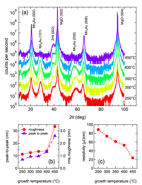
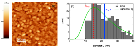
In Figure 1 (a) we show x-ray diffraction measurements of Mn2Au films grown at different substrate temperatures. Pure phase Mn2Au is found for all temperatures between 250∘C and 450∘C. However, the preferential orientation of the grains is improved as the temperature is increased, eventually giving pure (001)-oriented films at 450∘C. The Mn2Au tends to become rough at high deposition temperatures (Fig. 1 (b)), so that the Mn2Au film used in this study was deposited at 300∘C, which results in a compromise between smoothness of the film and crystal quality. The resistivity is rather large (, cf. Fig. 1 (c)) and shows only weak temperature dependence (not shown), so that our constant-voltage source can be treated as a constant-current source and the current density can be simply obtained from Ohm’s law with the room-temperature resistance value. In Figure 2 (a) we provide an AFM image of the film deposited at 300∘C. In Figure 2 (b), the manually evaluated grain size analysis is shown together with a lognormal fit to the histogram. The film has small grains with an average diameter of nm.
III Results
III.1 Experimental observation of switching in Mn2Au
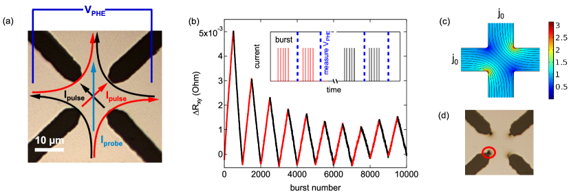
For the electrical measurements, an arbitrary waveform generator (Agilent 33522A) with a differential broadband amplifier (Tabor Electronics 9260) was used as the voltage source, and a Keithley 2182A Nanovoltmeter was used to measure the planar Hall voltage . Simple Hall crosses were used where the current was driven through all arms simultaneously as depicted in Figure 3 (a). The switching of the pulse and probe current lines was done with PhotoMOS relais. Temperature-dependent measurements were performed in a closed-cycle He cryostat. A duty cycle of 0.01 and an additional wait time of 1 s before taking the reading were found to be sufficient to remove cumulative thermal effects within the pulse bursts. Current pulse bursts with pulse widths between 100 ns and 10 ms were sent through the crosses and the planar Hall resistance was monitored to observe the switching as sketched in the inset of Figure 3(b). The bursts were programmed as to keep the transferred charge per burst constant, i.e., at larger current density , the number of pulses per burst is reduced. As shown in Figure 3(b), clear piecewise linear changes of the transverse resistance are seen at a current density of and pulse width of s, which changes sign when the current pulse direction is switched between two orthogonal directions, similar to the original experiment by Wadley et al. Wadley2016 A finite-element simulation of the current flow in our experiment shows that the current is very inhomogeneous and hot-spots at the corners of the Hall crosses occur (Figure 3(c)), which is supported by an optical micrograph of a burnt structure after applying heavy electrical stress (Figure 3(d)). In all measurements, we find larger switching amplitudes in the first few cycles on a given Hall cross compared to later cycles, where the amplitude remains essentially constant, cf. Fig. 3(c). This is explained by the switching in the hot-spots, which see only one current direction in the experiment, so that the Néel vector is reoriented only once and will remain aligned for all further cycles.
III.2 Macroscopic Model
A systematic investigation of the PHE resistance change (the switching amplitude) per transferred charge as functions of pulse width and current density reveals a very strong dependence of the switching amplitude on either quantity, both suggesting that thermal activation plays a crucial role in the Néel-order reorientation process. To elucidate the role of the thermal activation, we propose a macroscopic model to describe the switching.
To model the Néel-order spin-orbit torque switching, we need to describe the current-induced effective field, the energy barrier for the switching, the Joule heating of the current, and the relation between the Néel vector orientation and the planar Hall effect. The energy density of the Néel vector in a single biaxial antiferromagnetic grain due to the staggered spin-orbit field is Roy2016 ; Gomonay2016
| (1) |
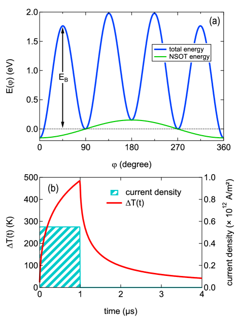
with the staggered effective field, which lies in the film plane and is oriented perpendicular to the current. denotes the in-plane biaxial magnetocrystalline anisotropy energy density within the tetragonal (001) plane and is the angle of with respect to an easy axis in the (001) plane. is the grain volume, is the current density in the film plane, is the unit vector along the -axis perpendicular to the fim plane, is the spin-orbit torque efficiency given as the effective staggered field per unit current density and is the unit cell volume. The first term is the usual magnetocrystalline energy, whereas the second term describes the Zeeman energy of the staggered magnetic moments in the staggered spin-orbit effective field. The angular dependence of the energy is exemplarily shown in Fig. 4. The Zeeman energy stabilizes the Néel vector such that the sublattice moments will align with the staggered effective field, i.e. perpendicular to the current direction. Because of the very strong exchange interaction in Mn2Au, each grain is assumed to possess collinear magnetic moments and has to rotate the Néel vector coherently (the macrospin approximation). A strong in-plane anisotropy is assumed and magnetization components pointing along the -axis are neglected Barthem2013 ; Barthem2016 .
The energy barrier is obtained as the minimum barrier for either the clockwise (cw) or counter-clockwise (ccw) rotation from an initial state to a final state :
| (2) |
This is sketched in Figure 4 (a) for the case of a switching event from a configuration with to . The switching rate for the switching of the Néel vector of an individual grain into a different orientation is given by the Néel-Arrhenius equation
| (3) |
with the attempt rate , the Boltzmann constant and the absolute temperature . A similar approach was used to describe the dependence of the antiferromagnetic blocking temperature on the magnetocrystalline anisotropy in exchange bias systems OGrady2010 . The switching is described by the Poisson distribution, so that the switching probability with an electrical pulse of length can be written as
| (4) |
The attempt rate represents the picosecond dynamics of the antiferromagnet, i.e. the ultrafast precession of the sublattice magnetic moments about the exchange field Gomonay2016 ; Roy2016 . This description is purely kinetic and is valid for sufficiently long pulse widths , such that the dynamics of the switching can be neglected Roy2016 . The influence of the Joule heating of the current density is taken into account by a two-dimensional model as derived by You et al.You2006 The Hall cross temperature rise as a function of time is given as
| (5) |
Here, is the film thickness, is the current line width, is the electrical conductivity, , , and are the mass density, specific heat, and heat conductivity of the substrate, respectively. The parameter is chosen as suggested by You et al. In Figure 4 (b) we exemplarily show the film temperature rise for a pulse. The temperature in Eq. 3 is taken as , where is the base temperature of the measurement. Temperature dependences of the substrate parameters are neglected. The orientation of the Néel vector is represented by a polar angle . With this angle, the planar Hall resistance in our cross geometry is written as where the prefactor is equivalent to the AMR amplitude .
To find the switching current density at which the switching from an initial state into the energetically favorable orthogonal state becomes deterministic, i.e. at which the barrier becomes zero, we need to find the current density at which the local minima of the energy become saddle points. By simultaneously solving and , we obtain
| (6) |
For small current density, such that , the local maxima of the total energy are located at and the barrier is simply , with , , or , depending on the combination of initial and final states. Only combinations with are energetically favorable and facilitated by the current. The lowest barrier is found for the switching from to , i.e. . Solving for the current density, we obtain
| (7) |
For small switching probability (linear response), one can further expand the exponential and obtains . Assuming an initially uniform occupation of the four easy-axis configurations and assuming all grains are equal, the planar Hall resistance change reads . Therefore, we obtain for the planar Hall resistance change per pulse in the linear response regime
| (8) |
In this regime, we expect to find a linear dependence of the switching amplitude on the pulse width. The switching amplitude is predicted to depend exponentially on the current density and also exponentially on the measurement temperature.
.
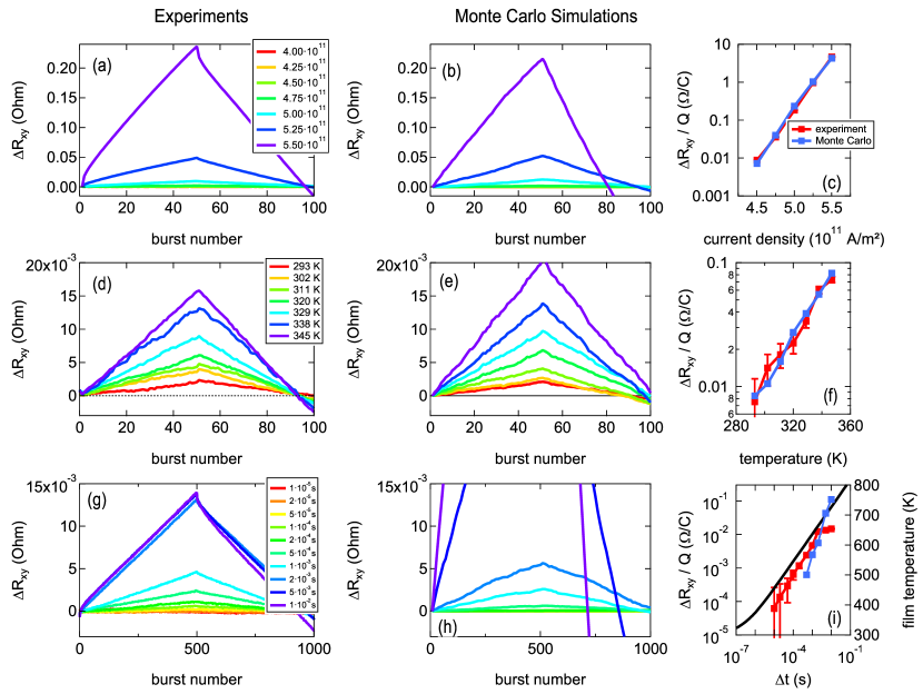
To fully take into account the influence of the pulse sequence and the film temperature due to the Joule heating, numerical simulations were performed with a Monte Carlo technique. An ensemble of grains with Néel vector orientations evenly distributed among the four easy-axis configurations was set-up. Optionally, the grain sizes can be taken from any distribution, e.g., a lognormal distribution. Here, only one fixed grain diameter is considered, which is treated as a phenomenological parameter. We use the average grain diameter as obtained by AFM, i.e. . The time-evolution of the film temperature is taken into account by a time-discretization scheme, such that multiple kinetic Monte Carlo trials are done for each pulse during heat-up (with current applied) and cool-down (without current) phases. For each trial, a random trial configuration is set up and its energy barrier according to Eq. III.2 and the switching probability according to Eq. 4 are computed for each grain independently. Random numbers are generated for each grain and the switching into the trial state is accepted if . The pulse burst patterns from the experiment are implemented in the model calculations to accurately reflect the experimental conditions and allow for a one-to-one comparison between the simulated and the experimental data sets. The model allows the Néel vector to switch into any easy-axis configuration, however, the probability to do so is larger if the sublattice magnetic moments are parallel to the staggered effective field. Thus, also thermally activated back-hopping is included in the model.
All quantities entering into the equations can in principle be obtained from experiments or ab initio calculations. We take and Barthem2013 . The film had a resistivity of and the thermal parameters of the MgO substrate are taken from Ref. Stackhouse2010 (cf. Fig. 4). The attempt rate is taken as .Arana2017 The core region of the Hall cross has a resistance of about 20 and we estimate an AMR amplitude of 5 % based on our observations, so that the planar Hall effect amplitude is . This estimate is consistent with a recent calculation of the AMR in Mn2Au Bodnar2018 . The current density at the center of the constriction of the Hall cross is used in the calculations, i.e. , cf. Figure 3 (c). As is evident from Eq. 8, the products and can be directly obtained by fitting the measured switching amplitudes as a function of the current density. Good agreement with the experiment is obtained with . The parameters , , and are difficult to obtain individually and are treated as adjustable parameters that will be discussed in the following sections.
III.3 Model results
In Figures 5(a),(d),(g) we show measurements of the switching amplitude for variations of the current density, the base temperature, and the pulse width, in a side-by-side comparison with the corresponding Monte Carlo simulations in Figures 5(b),(e),(h) and the amplitudes per unit charge in Figures 5(c),(f),(i). The dependences on the current density and on the temperature are very well reproduced by the model calculations with reasonable choices for the anisotropy energy density, providing strong evidence for the central role of the thermal activation in the switching process. Specifically, the clear increase of the switching amplitude by increasing the base temperature of the measurement (Figure 5(d)) shows that enhanced film temperature due to Joule heating will enhance the switching amplitude. For comparison, we performed calculations of the pulse width and current density variations without including the effect of Joule heating (not shown). In that case, the dependence on the current density is much less pronounced and the dependence on the pulse width (keeping the transferred charge per burst constant) will vanish completely, in contrast to the experiment. The switching amplitude increases exponentially with current density and temperature which is easily seen in the logarithmic plots in Figures 5(c),(f). The model reproduces these exponential dependencies quite accurately. The discrepancies between the experiments and the model calculations are somewhat larger for the pulse width dependence. As was shown by Fangohr et al., Equation III.2 has limited applicability for short wires as in the case of the present experiment Fangohr2011 . The maximum pulse duration within which acceptable results are expected is given by . In the present case, we estimate the limit to be 10 to 20 s, above which the film temperature increases less strongly than predicted by the formula due to the three-dimensional heat flow. Therefore, the pulse width dependence is not well reproduced by the model calculation, whereas the current density and temperature dependences taken with a pulse width of 1 s are very well described by the model. The saturation of the switching amplitude seen in the experimental pulse width dependence can thus be traced back to a saturation of the film temperature as a result of the three-dimensional heat flow.
III.4 Discussion
Without a current applied, the energy barrier is simply . Thus, the thermal stability factor at room temperature is large enough to ensure a stable Néel-state over time scales of more than ten years, and meets an important prerequisite for permanent magnetic memories Khvalkovskiy2013 . By measuring the grain size distribution with atomic force microscopy, we found the average grain diameter and, correspondingly, . From a recent measurement of the antiferromagnetic zone-center magnon modes by Brillouin light scattering, Arana et al. obtained a basal-plane anisotropy field of Arana2017 , i.e. and is in fair agreement with our estimate. However, our simulations taking the lognormal distribution as obtained from the AFM image into account disagree with the experiment: less pronounced dependences of the switching amplitude on temperature and current density are expected in that case (not shown). Assuming the anisotropy energy density obtained by Arana et al. is also valid for our samples, the corresponding grain diameter is , which is significantly larger than most of the observed grains. Both discrepancies can be explained by assuming that antiferromagnetic domains are formed across grain boundaries, thus smaller grains are stabilized by the intergranular exchange interaction and are harder to switch. However, we note that our model does not provide an understanding of the microscopic switching behaviour and does not allow to draw detailed conclusions about the formation of antiferromagnetic domains, which have to be obtained by other means. With the present estimates for the grain or domain size, we can estimate the spin-orbit torque efficiency as , where the higher value corresponds to the smaller grains and agrees reasonably well with the calculated value of by Železný et al. Zelezny2014 The current density for deterministic switching can be written as . All parameters entering into this expression are accessible from the experiment and is independent of the grain volume. Because of the strong heating that destroys the films, this curent density is experimentally only accessible with ultrafast current pulses Olejnik2018 .
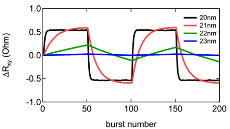
In Figure 6 we show the strong sensitivity of the switching amplitude on the grain diameter. Increasing the grain diameter by 4 nm, one can tune the switching behaviour from saturated to essentially not switchable at a given set of experimental conditions. The grain size and the film thickness are thus critical parameters for the NSOT switching. Due to the high film temperature, the switching amplitude is suppressed, because switching into energetically unfavorable configurations is facilitated through thermal activation. The initial kinks in the switching seen, e.g., in Figure 5(a) are hereby explained by the presence of a small number of smaller grains that are easy to saturate, whereas the majority of the grains show the linear behaviour far off saturation. The apparently exponential saturation observed by Wadley et al. in CuMnAsWadley2016 is explained by our model as a consequence of the stochastical nature of the switching process and the underlying Poisson probability distribution.
IV Conclusion
To summarize, we prepared epitaxial Mn2Au films and demonstrated the electrical switching of the Néel vector. A simple expression for the switching energy barrier was proposed and implemented into a principally parameter-free Monte Carlo model, which shows quantitative agreement with the measurements with realistic model parameters. The analytic expression for the transverse resistance change provides a transparent picture of the influence of the individual experimental parameters. The Joule heating of the current plays a key role for the switching process, as it provides sufficient thermal activation to reorient the Néel vector with the weak spin-orbit torque. The switching energy barrier in Mn2Au is large enough to retain the magnetic state over many years at room temperature, and is suitable for a practical application in antiferromagnetic spintronic devices.
Acknowledgements.
The authors thank G. Reiss for making available the laboratory equipment. They further thank D. Kappe for providing the finite-element simulation of the Hall cross device.References
- (1) J. Železný, H. Gao, K. Vyborny, J. Zemen, J. Masek, A. Manchon, J. Wunderlich, J. Sinova, and T. Jungwirth, Relativistic Néel-Order Fields Induced by Electrical Current in Antiferromagnets, Phys. Rev. Lett. 113, 157201 (2014).
- (2) T. Jungwirth, X. Marti, P. Wadley, and J. Wunderlich, Antiferromagnetic spintronics, Nat. Nanotechnol. 11, 231 (2016).
- (3) P. E. Roy, R. M. Otxoa, and J. Wunderlich, Robust picosecond writing of a layered antiferromagnet by staggered spin-orbit fields, Phys. Rev. B 94, 014439 (2016).
- (4) O. Gomonay, T. Jungwirth, and J. Sinova, High Antiferromagnetic Domain Wall Velocity Induced by Néel Spin-Orbit Torques, Phys. Rev. Lett. 117, 017202 (2016).
- (5) O. Gomonay, T. Jungwirth, and J. Sinova, Concepts of antiferromagnetic spintronics, Phys. Status Solidi RRL 11, 1700022 (2017).
- (6) P. Wadley et al., Electrical switching of an antiferromagnet, Science 351, 587 (2016).
- (7) V. M. T. S. Barthem, C. V. Colin, H. Mayaffre, M.-H. Julien, and D. Givord, Revealing the properties of Mn2Au for antiferromagnetic spintronics, Nat. Commun. 4, 2892 (2013).
- (8) P. Wadley et al., Tetragonal phase of epitaxial room-temperature antiferromagnet CuMnAs, Nat. Commun. 4, 2322 (2013).
- (9) M. J. Grzybowski, P. Wadley, K. W. Edmonds, R. Beardsley, V. Hills, R. P. Campion, B. L. Gallagher, J. S. Chauhan, V. Novak, T. Jungwirth, F. Maccherozzi, and S. S. Dhesi, Imaging Current-Induced Switching of Antiferromagnetic Domains in CuMnAs, Phys. Rev. Lett. 118, 057701 (2017).
- (10) K. Olejník, T. Seifert, Z. Kašpar, V. Novák, P. Wadley, R. P. Campion, M. Baumgartner, P. Gambardella, P. Němec, J. Wunderlich, J. Sinova, P. Kužel, M. Müller, T. Kampfrath, and T. Jungwirth, Terahertz electrical writing speed in an antiferromagnetic memory, Sci. Adv. 4, eaar3566 (2018).
- (11) S. Y. Bodnar, L. Šmejkal, I. Turek, T. Jungwirth, O. Gomonay, J. Sinova, A. A. Sapozhnik, H.-J. Elmers, M. Kläui, and M. Jourdan, Writing and reading antiferromagnetic Mn2Au by Néel spin-orbit torques and large anisotropic magnetoresistance, Nat. Commun. 9, 348 (2018).
- (12) M. Jourdan, H. Brüning, A. Sapozhnik, H.-J. Elmers, H. Zabel, and M. Kläui, Epitaxial Mn2Au thin films for antiferromagnetic spintronics, J. Phys. D. Appl. Phys. 48, 385001 (2015).
- (13) V. M. T. S. Barthem, C. V. Colin, R. Haettel, D. Dufeu, and D. Givord, Easy moment direction and antiferromagnetic domain wall motion in Mn2Au, J. Magn. Magn. Mater. 406, 289 (2016).
- (14) K. O’Grady, L. E. Fernandez-Outon, and G. Vallejo-Fernandez, A new paradigm for exchange bias in polycrystalline thin films, J. Magn. Magn. Mater. 322, 883 (2010).
- (15) C.-Y. You, I. M. Sung, B.-K. Joe, Analytic expression for the temperature of the current-heated nanowire for the current-induced domain wall motion, Appl. Phys. Lett. 89, 222513 (2006).
- (16) S. Stackhouse, L. Stixrude, B. B. Karki, Phys. Thermal Conductivity of Periclase (MgO) from First Principles, Rev. Lett. 104, 208501 (2010).
- (17) H. Fangohr, D. S. Chernyshenko, M. Franchin, T. Fischbacher, and G. Meier, Joule heating in nanowires, Phys. Rev. B 84, 54437 (2011).
- (18) M. Arana, F. Estrada, D. S. Maior, J. B. S. Mendes, L. E. Fernandez-Outon, W. A. A. Macedo, V. M. T. S. Barthem, D. Givord, A. Azevedo, and S. M. Rezende, Observation of magnons in Mn2Au films by inelastic Brillouin and Raman light scattering, Appl. Phys. Lett. 111, 192409 (2017).
- (19) A. V. V. Khvalkovskiy et al., Basic principles of STT-MRAM cell operation in memory arrays, J. Phys. D.: Appl. Phys. 46, 074001 (2013).