Development of a novel single-channel, 24 cm2, SiPM-based, cryogenic photodetector
Abstract
We report on the realization of a novel SiPM-based, cryogenic photosensor with an active area of 24 cm2 that operates as a single-channel analog detector. The device is capable of single photon counting with a signal to noise ratio better than 13, a dark rate lower than cps/mm2 and an overall photon detection efficiency significantly larger than traditional photomultiplier tubes. This development makes SiPM-based photosensors strong candidates for the next generation of dark matter and neutrino detectors, which will require multiple square meters of photosensitive area, low levels of intrinsic radioactivity and a limited number of detector channels.
Index Terms:
SiPM arrays, large photodetectors, photon counting, cryo-electronics, low-noise electronics.I Introduction
The excellent single-photon resolution, photon detection efficiency, cryogenic performance and cost of silicon photomultipliers (SiPMs) makes them appealing replacements for conventional photomultiplier tubes in next generation physics experiments. However, SiPMs typically have active areas of several tens of square millimeters, meaning a large number of devices is required to instrument the area of a single photomultiplier tube. This poses significant space and interconnection challenges in large experiments, where readout cables are long and front-end electronics must be placed in close proximity to the detector. An extra layer of complication arises in rare-event searches, such as those searching for neutrinoless double-beta decay or dark matter, where the background contributions from cables and electronics are often dominant. One way to alleviate this problem is to group SiPMs together to reach a surface area equivalent to a photomultiplier tube and read them out as a single channel device. However, the high capacitance of SiPMs, about , makes it challenging to operate a large array of SiPMs as a single channel device while maintaining adequate timing resolution and single photon resolution.
I-A Goals
This article focuses on the realization of a cryogenic, single analog output, SiPM-based photodetector with an active area comparable to a photomultiplier tube (PMT) and better performance in terms of photon detection efficiency (PDE) and single photon resolution.
The SiPM layout and the front-end electronics have been designed to achieve a signal to noise ratio (SNR), defined here as the ratio between the amplitude of the single photo-electron signal and the standard deviation of the baseline noise, better than 10. At this noise level, the rate of baseline fluctuations misidentified as signals is well below the intrinsic dark rate of the SiPMs and the detector can operate as a single photon counter (see Section IV-D). In addition, the high bandwidth front-end electronics maintain the fast peak of the SiPM signals and allow for better than timing resolution at 1 standard deviation. Finally, the overall power consumption of the front-end electronics is less than , which avoids excessive heat dissipation into the detector’s cryogenic operating environment. This is comparable to the cryogenic PMTs used in the DarkSide-50 detector which dissipate around plus an additional from the cryogenic pre-amplifier [1].
I-B Detector overview
The photodetector consists of 24 SiPMs mounted on a substrate, referred to hereafter as a SiPM tile, mated to a board housing the front-end electronics. The SiPM tile is subdivided into quadrants and each quadrant is read out with an independent low-noise transimpedance amplifier (TIA) based on an LMH6629 high-speed operational amplifier [2]. The four TIA outputs are then summed by a second stage amplifier into a single analog output that is extracted from the cryogenic environment. The SiPM tile partitioning is driven by a compromise between a limit on the total power dissipation of the detector, equivalent to the total number of TIAs, and the bandwidth and SNR attainable for a given detector capacitance.
I-C Cryogenic testing setup
The development and testing of the front-end electronics was done in a liquid nitrogen filled dewar with a flanged top. The dewar is sealed with a cover plate instrumented with a set of electrical and optical vacuum feedthroughs for power and signal lines and a calibration light source. A Keithley 2450 source measure unit was used for the SiPM bias voltage and a low-noise Elind 32DP8 power supply was used for the front-end amplifiers.
II SiPM Tile
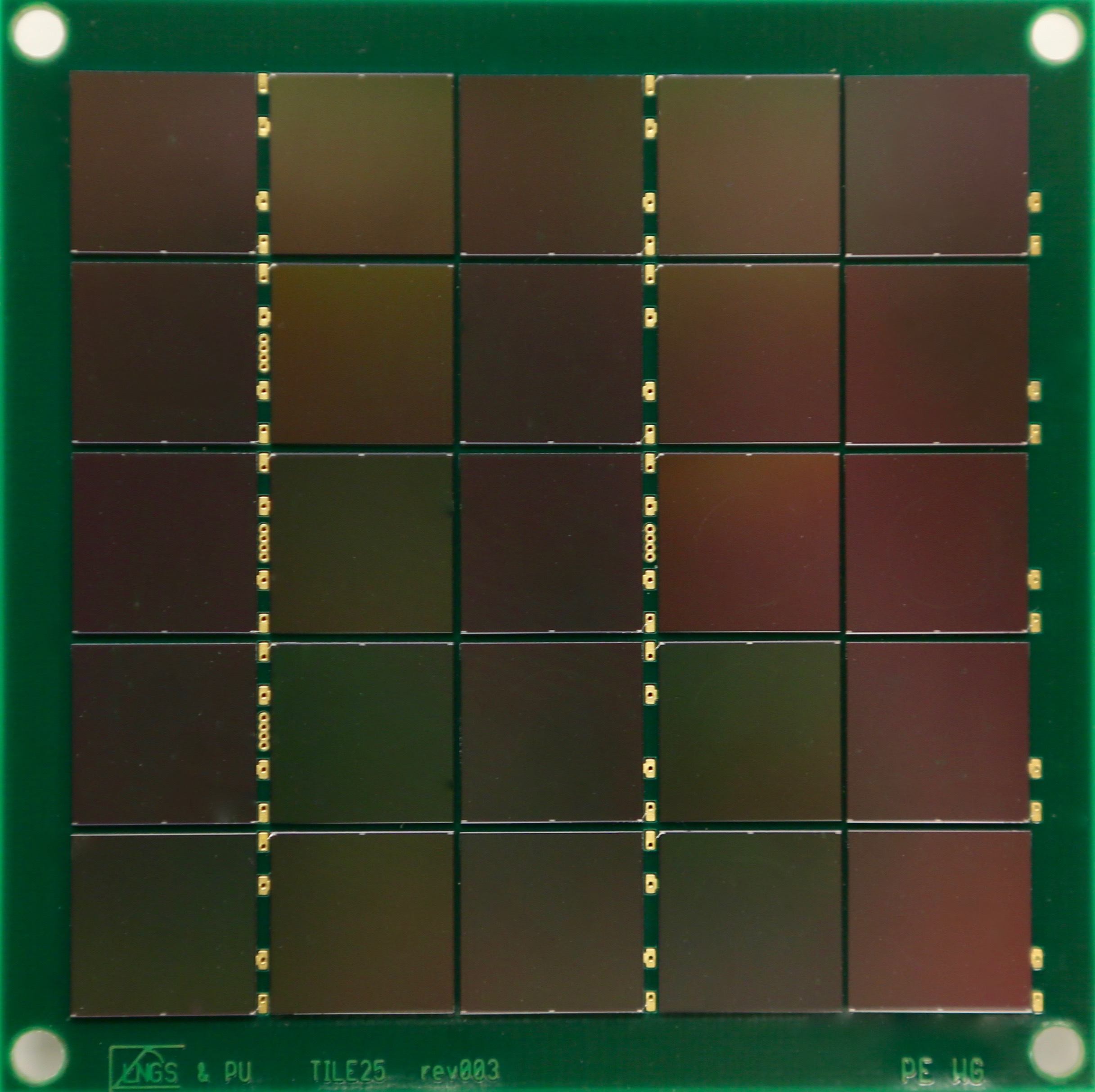
The SiPM tile is populated with NUV-HD-LF SiPMs produced by Fondazione Bruno Kessler (FBK) for the DarkSide-20k collaboration [3]. NUV-HD SiPMs have a peak efficiency of about in the near-ultraviolet, between , and are fabricated with a cell border structure that allows for high-density packing of small cell sizes [4]. The low-field (LF) variant of NUV-HD SiPMs have a lower field in the avalanche region, reducing the field-enhanced dark count rate relative to standard field NUV-HD SiPMs [5]. The NUV-HD-LF devices used to fabricate the tile characterized in Section IV-D have cells and quenching resistors at room temperature. A comprehensive study of the performance of NUV-HD-LF SiPMs at cryogenic temperature can be found in [6]: at and with of over-voltage, the darkrate is about .
The SiPM parameters relevant to the design of the readout electronics are discussed in [7] and include the shape of the signal and the equivalent capacitance () and resistance () of the device. When operated in liquid nitrogen, and for frequencies around . The value of is negligible for frequencies above as described in [7].
SiPM dies are mounted on an FR4 printed circuit board (PCB) using EPO-TEK EJ2189-LV conductive, silver-loaded epoxy, which has been tested for mechanical and electrical stability after repeated thermal cycling in liquid nitrogen. The epoxy is screened onto the tile in a thick layer, creating a coplanar surface on which the SiPM dice are placed with a manual die bonder. The top side pad of the SiPM is wedge bonded with aluminum wire to a trace on the PCB. The anode and cathode of each SiPM are routed to a high density Samtec LSS-150-01-L-DV-A connector on the back-side of the PCB that mates with the front-end board.
The SiPM tile is shown in Figure 1. Neglecting the tile border, which was used to ease handling during testing, the tile has a fill factor in excess of , leading to an overall photon detection efficiency (PDE) at room temperature of about [5]. This can be compared to a traditional cryogenic Hamamatsu R11065 PMT, which has a quantum efficiency of at room temperature and an active to total surface area ratio of [8] (and the honeycomb packing loses an other ).
II-A SiPM topology
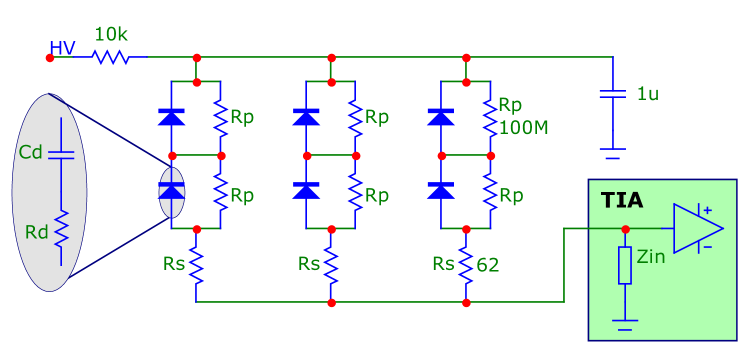
In an ideal TIA, the overall noise is proportional to the square root of the detector capacitance, 111This approximation is valid when the main contribution to the input equivalent noise is the voltage noise of the amplifier () and the other contributions (the current noise of the amplider, , and the Johnson-Nyquist noise of ) are negligible [9].. In order to reduce the noise, the detector capacitance seen by the TIA can be limited by arranging the SiPMs in series. However, due to capacitive coupling between the SiPMs, the signal will also be attenuated by a factor equal to the number of SiPMs in series. Theoretically, these two effects balance one another and the SiPM configuration does not affect the SNR.
In practice, several effects come into play that change the theoretical balance in favour of the configuration shown in Figure 2 (3 branches with 2 SiPMs in series each). First, the input impedance of the TIA () is non-zero. Therefore, a series resistance limits losses toward the inactive branches of the quadrant (the branches with no detected light): the relative losses can be calculated equal to , where is the complex impedance of the SiPM (which can be formulated in terms of and ). This is particularly important for high frequencies, e.g., the initial discharge of the SiPM, where can be large and small. Second, and effectively limit the noise gain to , breaking the overall noise dependence. Finally, the voltage noise at the TIA input includes the Johnson-Nyquist noise of . Increasing the number of SiPMs in series reduces the signal and increases the noise, affecting the SNR.
The tile is subdivided into four quadrants of six SiPMs, each readout by an independent TIA with the configuration shown in Figure 2. This configuration optimizes the SNR and bandwidth when compared to alternative arrangements with the same surface area.
II-B Bias voltage divider
At room temperature, the bias voltage across a series chain of SiPMs automatically equalizes due to the shared dark current between the devices [10]. The situation changes at cryogenic temperatures, where the SiPM dark rate drops below . At a gain of about , the dark current is only a few pA per device. In this regime, leakage currents dominate. The quiescent current flowing through the SiPMs was measured to be on the order of .
To ensure even bias distribution between the series SiPMs, a resistor-based voltage divider is added to the circuit as shown in Figure 2. Three points are critical to the design of the divider:
-
•
The precision of the divider has to compare with the desired gain uniformity () of the SiPMs. For and an over-voltage to bias ratio of about , the voltage partitioning accuracy has to be better than , which requires resistors with tolerance.
-
•
The current flowing through each voltage divider () has to be high enough so that a leakage current () from the SiPMs will not affect the voltage partitioning by more that the required gain uniformity. This is true when . Assuming an upper limit on the leakage current at liquid nitrogen temperature of , .
-
•
The shot noise of the total divider current () can significantly contribute to the intrinsic noise of the amplifier. As described in [7], the current noise () of the LMH6629 at corresponds to the shot noise produced by a current of about . Therefore it is advisable to maintain .
The SiPM tile uses tolerance, resistors that were binned by their resistance at room temperature to improve the resistance variation within each divider to better than .
III electronics
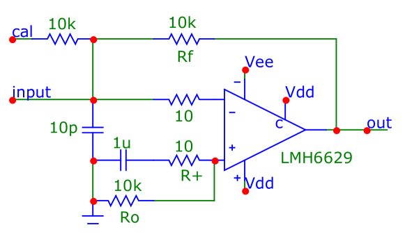
Each quadrant of the SiPM tile is readout by the TIA shown in Figure 3. This circuit is identical to the amplifier introduced in [7] with one relevant modification. The input bias current offset of the LMH6629 at cryogenic temperature depends strongly on the power supply voltage, see [7], which can cause low frequency noise and instability of the output offset. The standard solution to this problem is to match with and add a bypass capacitor to filter the noise introduced by . However, this would reduce the effectiveness of at dumping oscillations. Therefore, is left untouched and an offset compensation resistor equal in value to is added along with a filter capacitor.
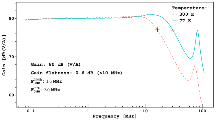
The gain and bandwidth of the TIA coupled with a SiPM tile quadrant are shown in Figure 4. The gain of the circuit is , as expected with , and a flatness of up to . The bandwidth in liquid nitrogen is .
III-A Noise model
The intrinsic voltage noise () of the LMH6629 at is , see [7]. The Johnson-Nyquist voltage noise from , and contribute an additional , resulting in a total input voltage noise term (equivalent to ). The voltage noise is amplified by the noise gain, which behaves like a high pass filter with and an asymptotic gain of (). This should result in an output noise spectrum that plateaus above at .
At , the intrinsic current noise of the LMH6629 is and the shot noise of the bias voltage divider, , is negligible. This results in an output noise density of , corresponding to a flat spectrum at . The Johnson-Nyquist current noise of in liquid nitrogen results in a second flat spectrum at . The sum of these two spectra in quadrature is . This current noise component only becomes significant below , where the output voltage noise drops by a few decades and, to first approximation, can be ignored.
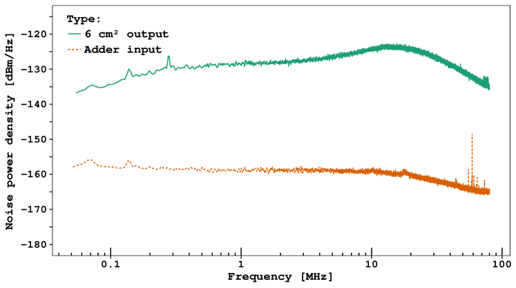
Figure 5 shows the output noise spectrum of the TIA and SiPM tile quadrant measured with an R&S FSV-7 spectrum analyzer at . The features predicted by the model are present. The noise density at is and . The peak at about in Figure 5 is not predicted by this simple noise model. The explanation of this peak is provided by the reduction of at high frequencies as discussed in Section II.
III-B Performance of the quadrant
The signal from the TIA once extracted from the dewar, is further processed at room temperature by a low-noise amplifier and then digitized by a 10 bit, 1 GS/s CAEN V1751 configured with a pre-trigger and a total gate time. The digitizer was triggered in coincidence with a light pulse from a Hamamatsu PLP-10 sub-nanosecond laser source. The output of the PLP-10 was attenuated so that an average of one photon was incident on the detector per pulse. The SiPMs were operated at an over-voltage of , corresponding to a gain of .
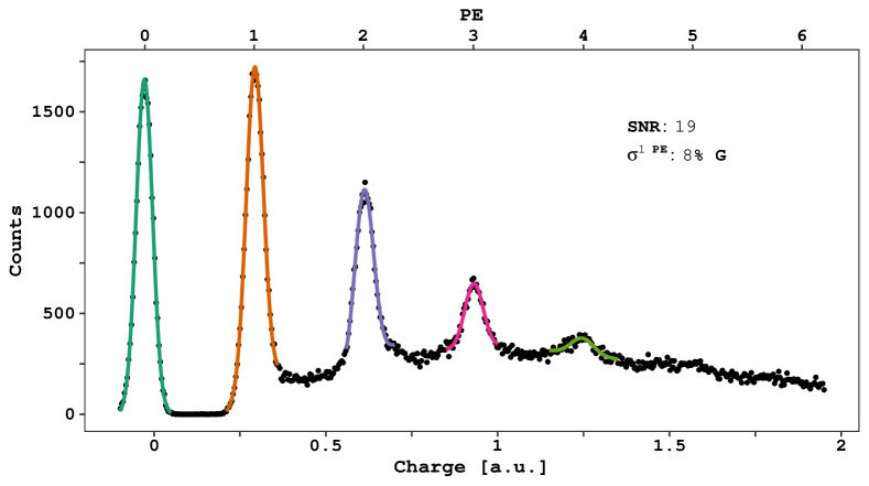
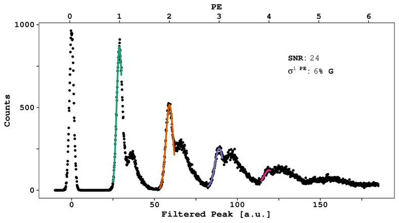
The amplitudes of the digitized waveforms were calculated offline using two different methods. Figure 7 shows the spectrum obtained using a fixed integration window of (). The baseline noise is of the gain and the separation between the photoelectron peaks is limited by after-pulsing of the SiPMs. Figure 7 shows the spectrum obtained using a matched filter algorithm [11], which results in an SNR of . The matched filter more clearly separates events with after-pulses from the photoelectron peaks, resulting in non-gaussian peak shapes.
IV Cryogenic Summing Amplifier
The output signals of the four TIAs from the four quadrants are combined at the input of a cryogenic summing amplifier that must amplify their sum for transmission across the dewar while maintaining the signal bandwidth, noise and dynamic range of the readout.
IV-A LMH6624 Cryogenic Characterization
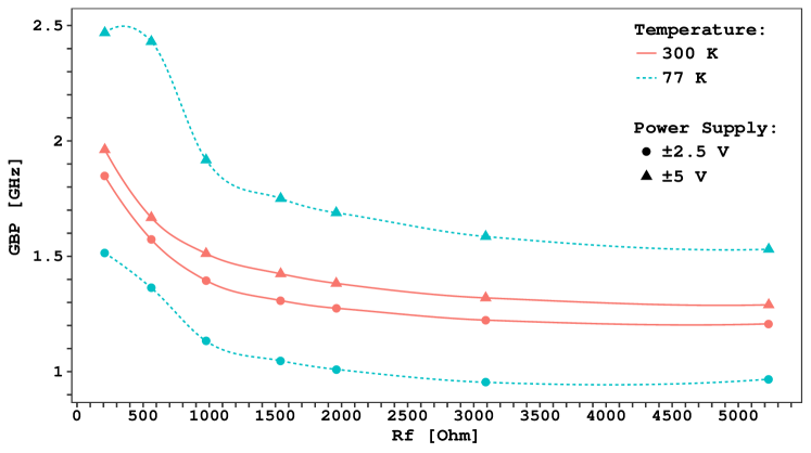
The core of the summing amplifier is an LMH6624 operational amplifier from Texas Instruments. At room temperature, the LMH6624 has a gain bandwidth product of and an input voltage noise of [12]. The LMH6624 was characterized in a liquid nitrogen bath following the procedure described in [7]. The input voltage noise density at drops to . Figure 8 shows the gain bandwidth product of the test circuit versus . At room temperature, the change in the gain bandwidth product due to the power supply voltage is relatively small, while in liquid nitrogen the variation is almost a factor of two. The overall shape of the curves is due to stray capacitance in the feedback path. The output compression point measured in liquid nitrogen is (before back-termination) with a quiescent current of respectively for power supplies.
IV-B Summing amplifier design
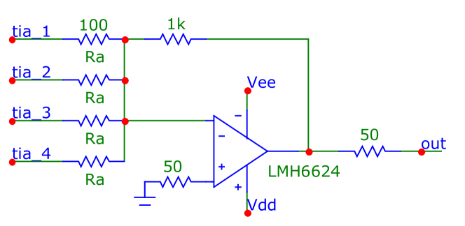
The summing circuit is shown in Figure 9. The input resistors () are to avoid over-loading the LMH6629 output stage. The signal gain is and the noise gain is [13]. The additional factor of ten amplification boosts the single photoelectron signal into the tens of millivolt range, simplifying the signal extraction and acquisition. The operational amplifier uses the same power supply as the TIAs.
The bandwidth of the circuit was measured with a Vector Network Analyzer (VNA) configured for S21 scan to be at room temperature and in liquid nitrogen. The electronic noise of the summing amplifier is dominated by the intrinsic voltage noise of the LMH6624 multiplied by the noise gain and the Johnson-Nyquist noise of the input resistors. The overall input equivalent noise of the amplifier is . Figure 5 compares the measured input equivalent noise spectrum of the amplifier to the output noise of the quadrant readout, demonstrating that the summing amplifier provides effectively no contribution to the overall noise of the system. In addition, the summing amplifier is slightly faster than the TIA and does not affect the bandwidth of the circuit. A back-termination is added to avoid signal reflections on the coaxial cable: its net effect is a factor of two reduction in gain and electronic noise.
IV-C Offset and dynamic range
The coherent sum of the current through all of the bias voltage dividers can produce a considerable offset at the output of the summing amplifier, which can be evaluated as . In the present configuration, this becomes after back-termination. Unfortunately, the amplified photoelectron signal is also positive (after two inversions) and the offset limits the dynamic range of the system to a few tens of photoelectrons. This was not a limitation for the present goal of performing low noise readout of a few photoelectrons. However, because offset contribution of the bias voltage divider is well known in advance, it is possible to bias the non-inverting pin of the amplifier and cancel the offset (or even further increase the negative offset). As an alternative, the authors are studying a rail to rail differential solution that would maximize the dynamic range.
IV-D Detector performance
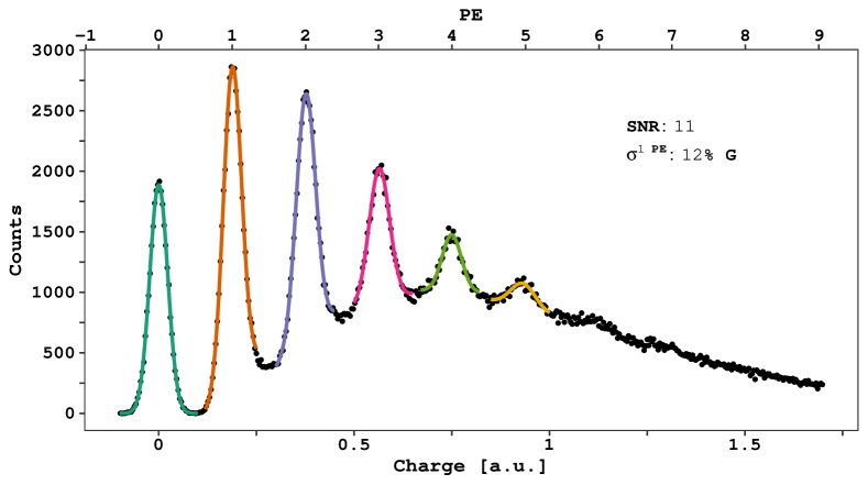
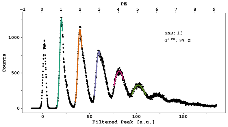
The signal extraction from the summing amplifier, its digitization and the analysis algorithms follow the methods used for the detector described in Section III-B. The spectrum from the fixed window integration is shown in Figure 11 and the matched filter spectrum is shown in Figure 11. In both cases, the SNR is greater than 10 and the gain uniformity meets the design goal, .
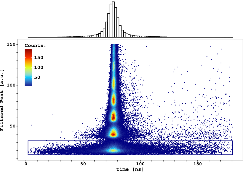
The timing of an event can be extracted from the peak time of the matched filtered waveform, as described in [7]. Figure 12 shows the event amplitude versus the reconstructed event time. The distribution of the reconstructed arrival time of the single photoelectron peak (top panel of Figure 12) contains a narrow central peak, with a standard deviation of about and non-gaussian tails that deteriorate the overall timing resolution to . These tails account for less than of the total events and are due to photoelectrons whose raw waveforms differ from the matched filter template. This is due to noise pickup jittering around the digitizer trigger, noise that, when coincident with the photoelectron signal, distorts the fast rising edge of the waveform and broaden the timing resolution.
V Conclusions
We report on the first implementation of electronics for a large area () single-channel, SiPM-based cryogenic photodetector with single photon sensitivity. This is achieved despite the large SiPM capacitance by subdividing the detector into four sub-arrays individually coupled to custom designed cryogenic transimpedance amplifiers. Signals from the four transimpedance amplifiers are then summed with a cryogenic summing amplifier to obtain a single-channel readout. Signals collected from the detector were analyzed using a matched filtering technique, resulting in an excellent signal to noise ratio () and timing resolution (). Moreover, the excellent overall PDE () and very low dark rate () make these devices ideal candidates for future, low-background cryogenic dark matter and neutrino detectors.
References
- [1] P. Agnes, I. F. M. Albuquerque, T. Alexander, A. K. Alton, K. Arisaka, D. M. Asner, M. Ave, H. O. Back, B. Baldin, K. Biery, V. Bocci, G. Bonfini, W. Bonivento, M. Bossa, B. Bottino, A. Brigatti, J. Brodsky, F. Budano, S. Bussino, M. Cadeddu, M. Cadoni, F. P. Calaprice, N. Canci, A. Candela, H. Cao, M. Caravati, M. Cariello, M. Carlini, S. Catalanotti, V. Cataudella, P. Cavalcante, A. Chepurnov, C. Cicalò, A. G. Cocco, G. Covone, L. Crippa, D. D’Angelo, M. D’Incecco, S. Davini, A. deCandia, S. DeCecco, M. DeDeo, G. DeFilippis, G. DeRosa, M. DeVincenzi, A. Derbin, A. Devoto, F. DiEusanio, C. Dionisi, G. DiPietro, E. Edkins, A. Empl, A. Fan, G. Fiorillo, K. Fomenko, G. Forster, D. Franco, F. Gabriele, C. Galbiat, S. Giagu, C. Giganti, G. K. Giovanetti, A. M. Goretti, F. Granato, L. Grandi, M. Gromov, M. Guan, Y. Guardincerri, B. R. Hackett, K. R. Herner, D. Hughes, P. Humble, E. V. Hungerford, A. Ianni, A. M. Ianni, I. James, T. N. Johnson, K. Keeter, C. L. Kendziora, V. V. Kobychev, G. Koh, D. Korablev, G. Korga, A. Kubankin, X. Li, M. Lissia, B. Loer, P. Lombardi, G. Longo, S. Luitz, Y. Ma, A. Machado, I. N. Machulin, A. Mandarano, S. M. Mari, J. Maricic, L. Marini, C. J. Martoff, P. D. Meyers, T. Miletic, R. Milincic, D. Montanari, A. Monte, M. Montuschi, M. E. Monzani, P. Mosteiro, B. J. Mount, V. N. Muratova, P. Musico, A. NavrerAgasson, A. Nelson, S. Odrowsk, A. Oleinik, M. Orsini, F. Ortica, L. Pagani, M. Pallavicini, E. Pantic, S. Parmeggiano, K. Pelczar, N. Pelliccia, A. Pocar, S. Pordes, D. A. Pugachev, H. Qian, K. Randle, G. Ranucci, M. Razeti, A. Razeto, B. Reinhold, A. L. Renshaw, M. Rescigno, Q. Riffard, A. Romani, B. Rossi, N. Rossi, S. D. Rountree, D. Sablone, P. Saggese, R. Saldanha, W. Sands, S. Sangiorgio, C. Savarese, B. Schlitzer, E. Segreto, D. A. Semenov, E. Shields, P. N. Singh, M. D. Skorokhvatov, O. Smirno, A. Sotnikov, C. Stanford, Y. Suvorov, R. Tartaglia, J. Tatarowicz, G. Testera, A. Tonazzo, P. Trinchese, E. V. Unzhakov, M. Verducci, A. Vishneva, R. B. Vogelaar, M. Wada, S. E. Walker, H. Wang, Y. Wang, A. W. Watson, S. Westerdale, M. M. Wojcik, X. Xiang, X. Xiao, J. Xu, C. Yang, J. Yoo, S. Zavatarelli, A. Zec, W. Zhong, C. Zhu, and G. Zuzel, “The Electronics, Trigger and Data Acquisition System for the Liquid Argon Time Projection Chamber of the DarkSide-50 Search for Dark Matter,” arXiv, 2017. [Online]. Available: http://arxiv.org/abs/1707.09889v1
- [2] Texas Instruments, “LMH6629 Ultra-Low Noise, High-Speed Operational Amplifier with Shutdown,” Texas Instruments, Tech. Rep., 2016. [Online]. Available: www.ti.com/lit/ds/symlink/lmh6629.pdf
- [3] C. E. Aalseth, F. Acerbi, P. Agnes, I. F. M. Albuquerque, T. Alexander, A. Alici, A. K. Alton, P. Antonioli, S. Arcelli, R. Ardito, I. J. Arnquist, D. M. Asner, M. Ave, H. O. Back, A. I. B. Olmedo, G. Batignani, E. Bertoldo, S. Bettarini, M. G. Bisogni, V. Bocci, A. Bondar, G. Bonfini, W. Bonivento, M. Bossa, B. Bottino, M. G. Boulay, R. Bunker, S. Bussino, A. F. Buzulutskov, M. Cadeddu, M. Cadoni, A. Caminata, N. Canci, A. Candela, C. Cantini, M. Caravati, M. Cariello, M. Carlini, M. Carpinelli, A. Castellani, S. Catalanotti, V. Cataudella, P. Cavalcante, S. Cavuoti, R. Cereseto, A. Chepurnov, C. Cicalò, L. Cifarelli, M. Citterio, A. G. Cocco, M. Colocci, S. Corgiolu, G. Covone, P. Crivelli, I. D’Antone, M. D’Incecco, D. D’Urso, M. D. Da Rocha Rolo, M. Daniel, S. Davini, A. De Candia, S. De Cecco, M. De Deo, G. De Filippis, G. De Guido, G. De Rosa, G. Dellacasa, M. Della Valle, P. Demontis, A. Derbin, A. Devoto, F. Di Eusanio, G. Di Pietro, C. Dionisi, A. Dolgov, I. Dormia, S. Dussoni, A. Empl, M. F. Diaz, A. Ferri, C. Filip, G. Fiorillo, K. Fomenko, D. Franco, G. E. Froudakis, F. Gabriele, A. Gabrieli, C. Galbiati, P. G. Abia, A. Gendotti, A. Ghisi, S. Giagu, P. Giampa, G. Gibertoni, C. Giganti, M. A. Giorgi, G. K. Giovanetti, M. L. Gligan, A. Gola, O. Gorchakov, A. M. Goretti, F. Granato, M. Grassi, J. W. Grate, G. Y. Grigoriev, M. Gromov, M. Guan, M. B. B. Guerra, M. Guerzoni, M. Gulino, R. K. Haaland, A. Hallin, B. Harrop, E. W. Hoppe, S. Horikawa, B. Hosseini, D. Hughes, P. Humble, E. V. Hungerford, A. M. Ianni, C. Jillings, T. N. Johnson, K. Keeter, C. L. Kendziora, S. Kim, G. Koh, D. Korablev, G. Korga, A. Kubankin, M. Kuss, B. Lehnert, X. Li, M. Lissia, G. U. Lodi, B. Loer, G. Longo, P. Loverre, R. Lussana, L. Luzzi, Y. Ma, A. A. Machado, I. N. Machulin, A. Mandarano, L. Mapelli, M. Marcante, A. Margotti, S. M. Mari, M. Mariani, J. Maricic, C. J. Martoff, M. Mascia, M. Mayer, A. B. McDonald, A. Messina, P. D. Meyers, R. Milincic, A. Moggi, S. Moioli, J. Monroe, A. Monte, M. Morrocchi, B. J. Mount, W. Mu, V. N. Muratova, S. Murphy, P. Musico, R. Nania, A. N. Agasson, I. Nikulin, V. Nosov, A. O. Nozdrina, N. N. Nurakhov, A. Oleinik, V. Oleynikov, M. Orsini, F. Ortica, L. Pagani, M. Pallavicini, S. Palmas, L. Pandola, E. Pantic, E. Paoloni, G. Paternoster, V. Pavletcov, F. Pazzona, S. Peeters, K. Pelczar, L. A. Pellegrini, N. Pelliccia, F. Perotti, R. Perruzza, V. P. Fortes, C. Piemonte, F. Pilo, A. Pocar, T. Pollmann, D. Portaluppi, D. A. Pugachev, H. Qian, B. Radics, F. Raffaelli, F. Ragusa, M. Razeti, A. Razeto, V. Regazzoni, C. Regenfus, B. Reinhold, A. L. Renshaw, M. Rescigno, F. Retiere, Q. Riffard, A. Rivetti, S. Rizzardini, A. Romani, L. Romero, B. Rossi, N. Rossi, A. Rubbia, D. Sablone, P. Salatino, O. Samoylov, E. S. García, W. Sands, M. Sant, R. Santorelli, C. Savarese, E. Scapparone, B. Schlitzer, G. Scioli, E. Segreto, A. Seifert, D. A. Semenov, A. Shchagin, L. Shekhtman, E. Shemyakina, A. Sheshukov, M. Simeone, P. N. Singh, P. Skensved, M. D. Skorokhvatov, O. Smirnov, G. Sobrero, A. Sokolov, A. Sotnikov, F. Speziale, R. Stainforth, C. Stanford, G. B. Suffritti, Y. Suvorov, R. Tartaglia, G. Testera, A. Tonazzo, A. Tosi, P. Trinchese, E. V. Unzhakov, A. Vacca, E. Vázquez-Jáuregui, M. Verducci, T. Viant, F. Villa, A. Vishneva, R. B. Vogelaar, M. Wada, J. Wahl, J. Walding, S. E. Walker, H. Wang, Y. Wang, A. W. Watson, S. Westerdale, R. Williams, M. M. Wojcik, S. Wu, X. Xiang, X. Xiao, C. Yang, Z. Ye, A. Y. de Llano, F. Zappa, G. Zappalà, C. Zhu, A. Zichichi, M. Zullo, and A. Zullo, “DarkSide-20: A 20 Tonne Two-Phase LAr TPC for Direct Dark Matter Detection at LNGS,” arXiv, 2017. [Online]. Available: http://arxiv.org/abs/1707.08145v1
- [4] C. Piemonte, F. Acerbi, A. Ferri, A. Gola, G. Paternoster, V. Regazzoni, G. Zappala, and N. Zorzi, “Performance of NUV-HD Silicon Photomultiplier Technology,” IEEE Trans. Elec. Dev., vol. 63, no. 3, pp. 1111–1116, 2016. [Online]. Available: http://ieeexplore.ieee.org/lpdocs/epic03/wrapper.htm?arnumber=7397984
- [5] A. Ferri, F. Acerbi, A. Gola, G. Paternoster, C. Piemonte, and N. Zorzi, “Performance of FBK low-afterpulse NUV silicon photomultipliers for PET application,” JINST, vol. 11, no. 03, pp. P03 023–P03 023, 2016. [Online]. Available: http://stacks.iop.org/1748-0221/11/i=03/a=P03023?key=crossref.3b90668de68c0dbe8d723d4154a2ece8
- [6] F. Acerbi, S. Davini, A. Ferri, C. Galbiati, G. Giovanetti, A. Gola, G. Korga, A. Mandarano, M. Marcante, G. Paternoster, C. Piemonte, A. Razeto, V. Regazzoni, D. Sablone, C. Savarese, G. Zappala, and N. Zorzi, “Cryogenic Characterization of FBK HD Near-UV Sensitive SiPMs,” IEEE Trans. Elec. Dev., pp. 1–6, 2017. [Online]. Available: http://ieeexplore.ieee.org/document/7807295/
- [7] M. D’Incecco, C. Galbiati, G. K. Giovanetti, G. Korga, X. Li, A. Mandarano, A. Razeto, D. Sablone, and C. Savarese, “Development of a very low-noise cryogenic pre-amplifier for large-area SiPM devices,” submitted to IEEE Transaction Nuclear Science, 2017. [Online]. Available: https://arxiv.org/abs/1706.04213
- [8] Hamamatsu, “R11065-10 Photomultiplier Tube Datasheet,” Hamamatsu, Tech. Rep., 2011.
- [9] Burr Brown, “Noise Analysis of FET Transimpedance Amplifiers,” Texas Instruments, Tech. Rep. [Online]. Available: http://www.ti.com/lit/an/sboa060/sboa060.pdf
- [10] W. Ootani, “Development of pixelated scintillation detector for highly precise time measurement in MEG upgrade,” Nuclear Instruments and Methods in Physics Research Section A: Accelerators, Spectrometers, Detectors and Associated Equipment, vol. 732, pp. 146 – 150, 2013, doi: 10.1016/j.nima.2013.07.043. [Online]. Available: http://www.sciencedirect.com/science/article/pii/S0168900213010528
- [11] G. Turin, “An introduction to matched filters,” IEEE Trans. Inform. Theory, vol. 6, no. 3, pp. 311–329, 1960. [Online]. Available: http://ieeexplore.ieee.org/document/1057571/
- [12] Texas Instruments, “LMH6624 and LMH6626 Single/Dual Ultra Low Noise Wideband Operational Amplifier,” Texas Instruments, Tech. Rep., 2014. [Online]. Available: http://www.ti.com/lit/ds/symlink/lmh6624.pdf
- [13] Analog Devices, “Op Amp Bandwidth and Bandwidth Flatness,” Analog Devices, Tech. Rep. [Online]. Available: http://www.analog.com/media/en/training-seminars/tutorials/MT-045.pdf