Parasitic Bipolar Leakage in III-V FETs: Impact of Substrate Architecture
Abstract
InGaAs-based Gate-all-Around (GAA) FETs with moderate to high In content are shown experimentally and theoretically to be unsuitable for low-leakage advanced CMOS nodes. The primary cause for this is the large leakage penalty induced by the Parasitic Bipolar Effect (PBE), which is seen to be particularly difficult to remedy in GAA architectures. Experimental evidence of PBE in In70Ga30As GAA FETs is demonstrated, along with a simulation-based analysis of the PBE behavior. The impact of PBE is investigated by simulation for alternative device architectures, such as bulk FinFETs and FinFETs-on-insulator. PBE is found to be non-negligible in all standard InGaAs FET designs. Practical PBE metrics are introduced and the design of a substrate architecture for PBE suppression is elucidated. Finally, it is concluded that the GAA architecture is not suitable for low-leakage InGaAs FETs; a bulk FinFET is better suited for the role.
Index Terms:
PBE, III-V, InGaAs, BTBTI Introduction
MOSFETS of various architectures based on InGaAs have been investigated by many authors as candidates for high-performance nFETs in advanced nodes [1],[2],[3]. The primary attraction of the InGaAs channel is the low transport mass of the valley, and the correspondingly high electron velocity. In spite of the low charge density (also a consequence of the small and isotropic -valley mass), InGaAs devices in the quasi-ballistic limit are theoretically expected to exceed on-state currents provided by Si-based FETs. However, the leakage characteristics of the InGaAs channel are very problematic. Due to the small and direct bandgap, InGaAs channels are prone to Band-to-Band Tunneling (BTBT), particularly at moderate to high voltages. As argued in [4], mobile SoC and server products require voltages in the 0.7-0.9V range. While the BTBT current itself presents a challenge (causing significant channel-to-drain GIDL leakage), the OFF-state leakage problem is made considerably worse by the Parasitic Bipolar Effect. The PBE occurs in devices in which the channel has a poor conductive path for the extraction of holes. The holes are generated during BTBT events in which valence electrons tunnel into the drain. The electron is swept into the drain contact, while the hole remaining in the channel must be either conductively extracted, or eventually recombine. In GAA (or similar) FETs, there is no direct conductive path between the channel and the substrate. Furthermore, the source-channel barrier in the off-state prevents holes from easily diffusing from the channel into the source. Holes accumulate in the channel (being continually generated by BTBT) until their positive charge sufficiently lowers the energy barrier. The barrier is sufficiently lowered when the hole current over the barrier matches the BTBT hole generation current. This steady-state condition therefore has a reduced barrier height for electrons which are diffusing from the source into the channel, increasing the off-state leakage. This is known as the Parasitic Bipolar effect, and has been described and observed both in Si [5] and III-V materials [6], [7]. It is of particular interest for advanced CMOS nodes because it is observed that the same device features which are needed for good electrostatic control at scaled Lg (i.e. GAA and similar structures) also greatly exacerbate PBE, as will be shown in this paper. This makes controlling PBE of critical importance.
II Device Structure
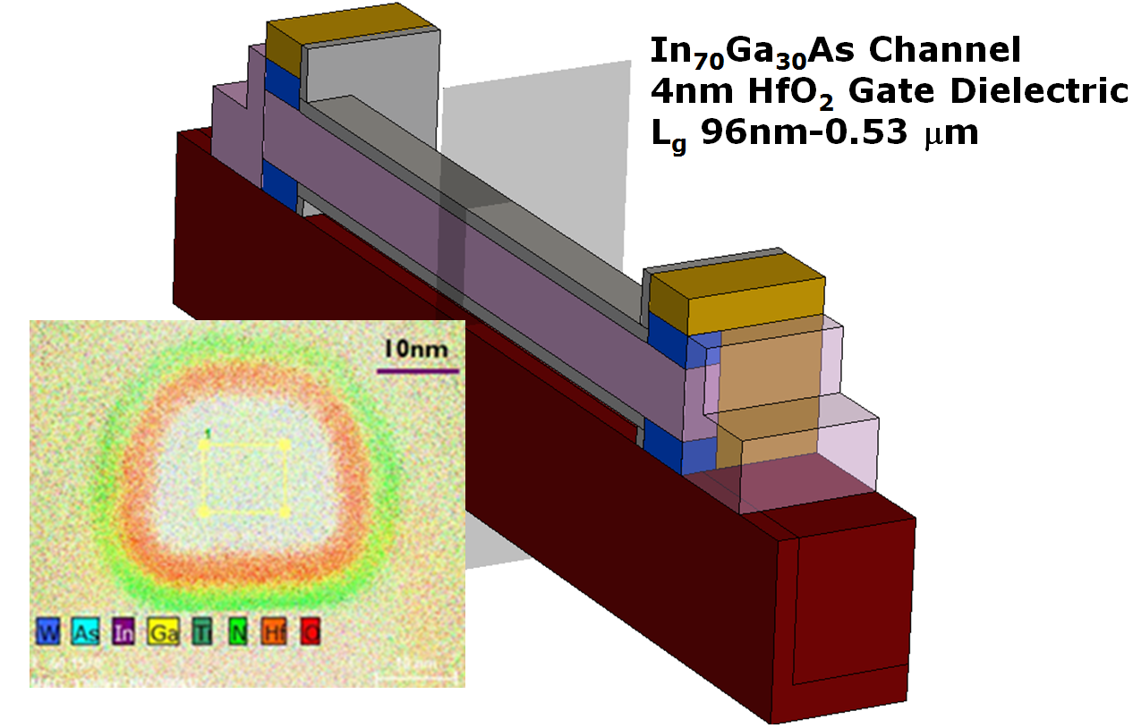
The measured device was a single-channel, rectangular nanowire GAA FET, with an In70Ga30As, utilizing a novel gate dielectric (the overall process is described in detail in [3]). A typical example of the device cross-section is illustrated in Fig. 1. Multiple channel lengths were fabricated, ranging from ’long’ channels of 0.53 m, down to the ’short’ Lg of 0.096 m. While the latter is much longer than the eventually desirable lengths (15-20 nm Lg for advanced CMOS nodes), it is sufficient for illustrating the challenges posed by PBE.
III Analysis of In70Ga30As GAA PBE
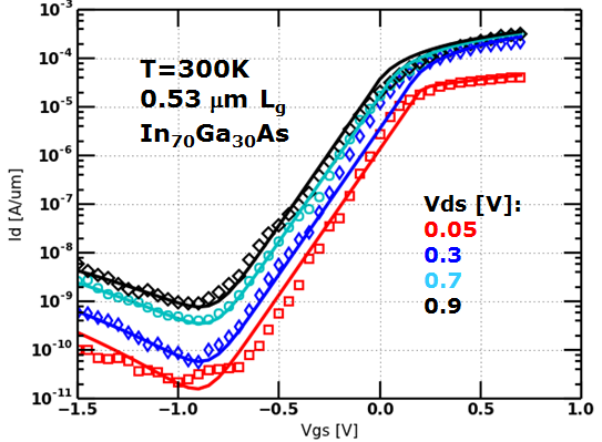
The presence and magnitude of PBE is difficult to ascertain directly from single-device data. The approach adopted in this work is to use simulation to match measured data as closely as possible, deducing the role played by PBE from the internal properties of the simulated devices. As the first step, the long channel device is simulated (Fig. 2). PBE is generally negligible for long channel devices (bipolar gain scaled inversely with channel length under ideal circumstances [7], faster in non-ideal devices). The degraded sub-threshold slope (SS) observed with the long-channel devices of Fig. 2 (approximately 120 mV/dec) is therefore attributed to the presence of Cit. Simulations indicate that in the absence of Cit, the long-channel undoped device would have nearly ideal SS (with a fully depleted channel). This enables the calibration of Cit for each measured device. Additionally, the leakage tails observed in Fig. 2 are attributed to pure BTBT (no PBE gain). It should be noted that the long-channel device has the characteristic ’GIDL checkmark’ shape for all VDS values. The sub-threshold slope is essentially constant and mostly independent of VDS, until the thermionic current intercepts the BTBT current. Comparison to simulation is used to calibrate BTBT parameters (a non-local dynamic path BTBT model (functionally identical to the model used in [8]) is used for the simulation; the basic parameters are from [9], with compositional and size-quantization corrections based on Tight-Binding simulations [10]; additional minor adjustments to the cross-section are used to match the data (some variation in cross-section from device to device is to be expected).
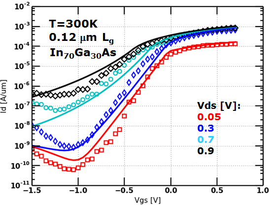
The OFF-state behavior of the short-channel device (Fig. 3) is strikingly different than that of the long-channel device. While the ’GIDL checkmark’ is still observed for low VDS values, there is a substantial increase and VDS dependence in the sub-threshold slope for all cases where VDS 0.3V. Matching this behavior in simulation requires PBE; electrostatic degradation through Dit does not produce the observed VDS behavior. Simulation also does not indicate the presence of punch-through at this moderate channel length (which would tend to manifest as a sharp change in SS at some point in sub-threshold; generally not a smooth increase as seen in the data). Reasonable agreement of simulation and data was only observed when simulating with PBE (this is actually automatic when simulating BTBT in a substrate-decoupled channel such as GAA; suppressing PBE in simulation actually requires post-processing BTBT current).
In order to rule out any possibility that the SS degradation with VDS is in fact caused by some unexpected trap behavior (and therefore not captured in the simulation), measurements of a short device (Lg=96 nm) were performed at low temperature (77K). At 77K, traps near the conduction band (CB) edge are essentially unoccupied in the OFF-state, significantly reducing the role of Dit on sub-threshold behavior. As can be seen in Fig. 4, the low-T and room-T behavior are very similar. While the overall SS values are reduced at low-T (as is to be expected for thermionic current), the VDS-dependent increase is still observed. It should also be noted that the BTBT-induced leakage floor is also lower at low-T. This is a consequence of the increased bandgap, and increased Fermi-blocking of tunneling events due to the degenerately occupied drain. However, while the overall leakage magnitude is reduced at low-T, the basic behavior of increasing SS with VDS continues to be observed. As was the case at room temperature, this behavior is qualitatively reproduced by simulation at low-T as well.
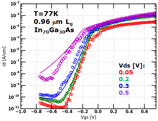
The match between simulation and data for the short-channel cases (Figs. 3 and 4) are reasonably good. In particular, the transition between the ’GIDL checkmark’ and the more flattened Id-VGS behavior of the PBE-dominated high VDS cases is difficult to capture precisely. In the presence of PBE, straightforward simulation indicates that all Id-Vg curves have the flattened behavior, with no uptick at very negative VGS values. However, recombination in the channel bulk and at the channel-dielectric interface reduces PBE gain. Interface recombination in particular becomes strong at very negative VGS (when the channel holes are attracted to the gate), and eventually suppresses PBE. When that happens, the ’GIDL checkmark’ is recovered. The standard surface recombination model [8] was used for the simulations (surface recombination velocities in the range of 1000-2000 cm/s are required for best agreement with measured data, much higher than would be expected in a Silicon process). Even qualitative agreement of the measured and simulated data in sub-threshold could only be accounted for with PBE.
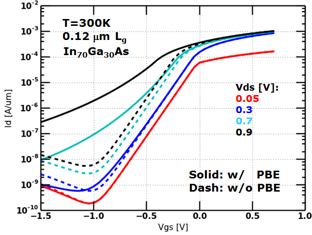
The impact of PBE on the device is most clearly seen in Fig. 5, where simulated Id-Vg curves for the short-channel FET are illustrated with and without PBE. The PBE-curves are identical to those of Fig. 3 and reasonably well-matched to data. The non-PBE curves are obtained by performing single-carrier simulation with no BTBT, then adding a post-processed BTBT current. Given that the BTBT currents themselves are quite low, this is tantamount to instantaneously extracting generated holes from the channel, i.e. a good approximation to PBE-free behavior without any structural changes (the alternative of adding a lead to the channel, or artificially increasing recombination, would have produced undesired simulation artifacts, and the interpretation of results would have been consequently more difficult). It is apparent that non-PBE simulations are not even rough approximations of the observed short-channel behavior, in spite of the good agreement at long channel. Secondly, it is also clear that the leakage penalty of PBE is quite severe for this device; 1-2 orders of magnitude in additional leakage are observed.
IV Physics of PBE Behavior
In the previous section it was mentioned that non-PBE BTBT leakage could be identified by the ’GIDL checkmark’ shape, whereas strong PBE tends to produce a much flatter Id-Vg curve. This qualitative difference can be used to discern PBE-controlled from non-PBE leakage. While the previous sections focused on In70Ga30As FETs in the 96 nm-500 nm Lg range for which measured data was available, this (and subsequent) sections examines the behavior of devices more suited for advanced CMOS nodes. The structures considered have an Lg of 15 nm, and utilize the less BTBT-prone In53Ga47As channel (an even better choice might be In35Ga65As, but BTBT leakage is so dramatically reduced for this low-In channel that In53Ga47As serves as a better illustration of the challenges involved.).
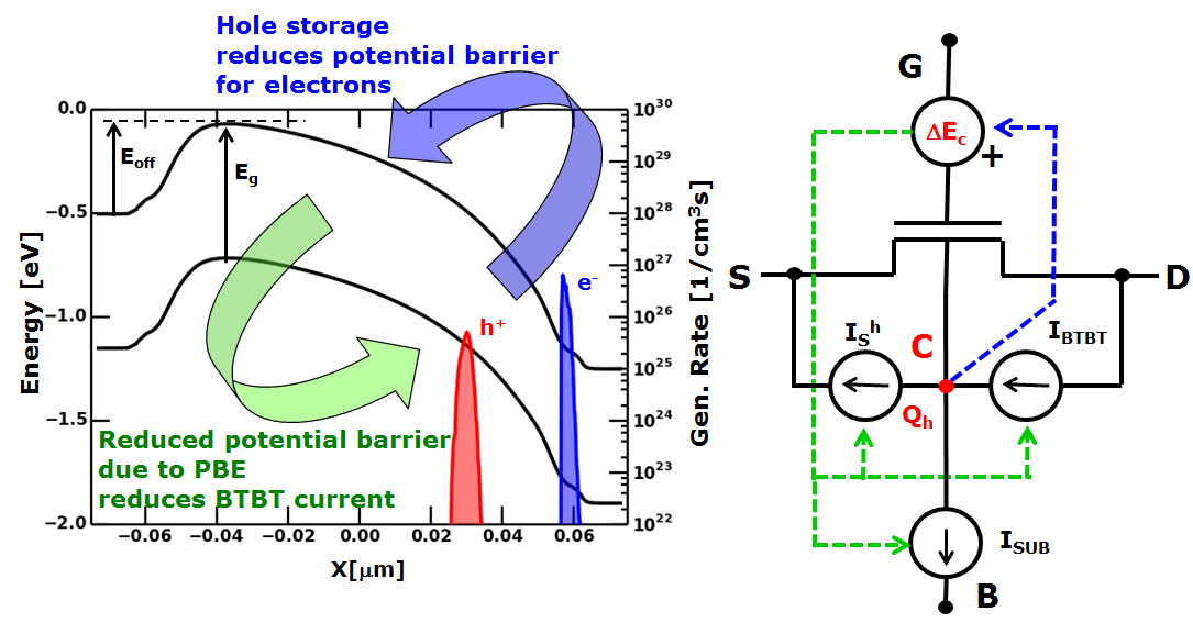
The PBE mechanisms can be thought of as a dual feedback loop, as illustrated in Fig. 6. The first and well-documented loop ([6], [7]) describes the buildup of the hole concentration in the channel, induced by the e-/h+ pair generation due to BTBT at the drain side of the channel. In steady-state, the generation of holes in the channel is balanced by the hole current across the channel-source barrier, the current through a substrate contact (if available), as well as bulk and surface recombination. The equation for current continuity at the ’C’ node of Fig. 6 is then
| (1) |
where is the excess hole charge and is the hole recombination time. It is evident from Fig. 6 and Eqn. 1 that the various hole current components are all functions of the CB modulation . This modulation in turn is a function of the accumulated hole charge, as governed by the device electrostatics. The conceptual model for capacitive coupling of the hole charge and the CB at the ’Top-of-the-Barrier’ (ToB) is illustrated in Fig. 7.

The accumulation of positive charge in the channel increases the ToB potential, but the extent to which it does so depends on the 3-D electrostatics of the device. With ideal electrostatic coupling of the gate to the ToB, PBE gain would be negligible (since the ToB potential would be perfectly pinned by the gate). In real devices, however, the details of the electrostatics must be taken into account. In this work, electrostatics are handled by 3-D Drift-Diffusion simulation. The simulated evolution of the PBE effect as a function of the threshold voltage (expressed as the Ioff target) is illustrated in Fig. 8. The large positive charge in the channel lowers the conduction band (CB) energy (also seen in Fig. 8), resulting in an increase in electron injection from the source. This is the ’standard’ PBE loop. However, Fig. 8 reveals a more subtle behavior: the CB lowering begins to saturate at a certain Vt (or equivalently, a certain VGS), with only minor subsequent increases in the hole concentration.
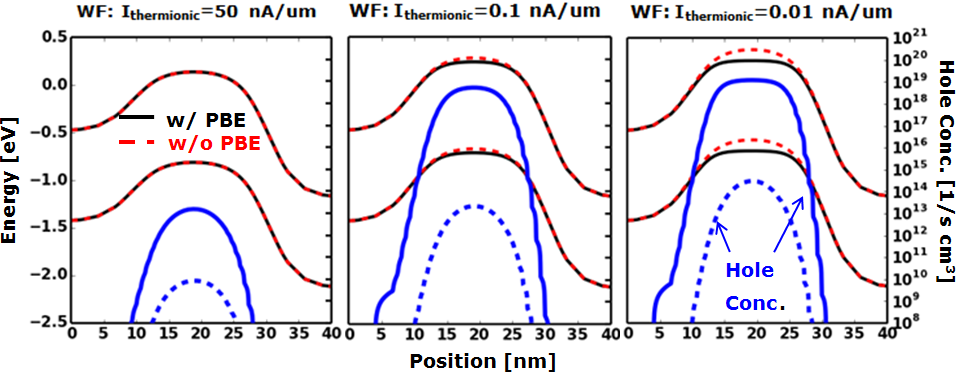
This occurs in spite of the fact that IBTBT is expected to increase with increasing Vt or increasingly negative VGS. The reason for this behavior can be gleaned from Fig. 6: the secondary feedback loop modulates IBTBT based on the shift in the CB. Specifically, as the CB is decreased due to PBE, IBTBT is likewise decreased due to a reduction in the tunneling window, as well as the effective thickness of the tunneling barrier at the drain side of the channel. This steep reduction of IBTBT with increasing PBE is illustrated in Fig. 9.
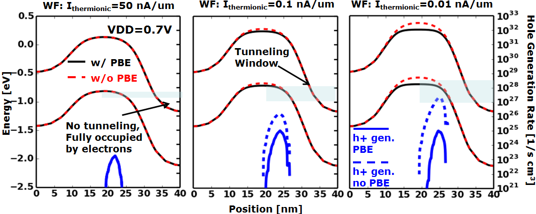
As can be seen in the progression of Vt values in Fig. 9, the FET with PBE exhibits a saturation of the hole generation rate with increasing Vt. This is in contrast to the non-PBE device (with a substrate contact) shown in the same Fig. 9, where the BTBT-induced hole generation rate keeps increasing with Vt (and likewise with increasing VGS). The saturating value of the hole concentration, CB lowering, and IBTBT with increasing Vt or gate bias are all consequences of the steady-state balance of the two feedback mechanisms.
IV-A Short-Channel Prediction
The predicted current behavior of the 15nm FET is discussed next. The Id-Vg characteristics are illustrated in Fig. 10.
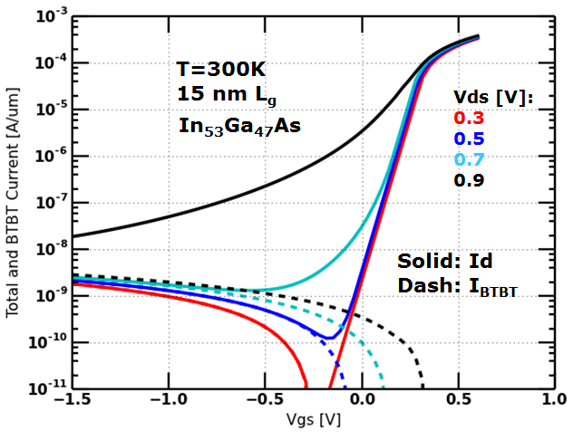
The large discrepancy seen between the total drain current and the BTBT current for moderate to large drain biases observed in Fig. 10 is of course due to PBE (as also reported in [6] and [7]). The standard metric for bipolar gain is defined as
| (2) |
where is the increase in drain current due to PBE, while IBTBT is the BTBT current itself. The bipolar amplification factor is often interpreted as the ‘leakage penalty‘ incurred due to PBE. However, this is not entirely correct since the presence of PBE alters BTBT itself (the second feedback loop). This is illustrated in the case of the 15nm device in Fig. 11.
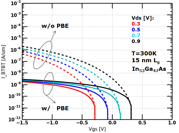
Due to the significant discrepancy between the BTBT currents with and without PBE, a more direct metric for the ‘PBE leakage penalty‘ is defined here as follows:
| (3) |
The gain of Eqn. 3 is the ratio of the drain current with and without PBE. The BTBT currents are of course very different for the two cases, as are the drain currents. The case with PBE corresponds to a real (measured or simulated) device, whereas the no-PBE case is an imaginary device in which the holes accumulating in the channel are instantly extracted. Given this definition, is necessarily a simulation-based metric. The behavior of and as functions of applied bias are illustrated in Fig. 12.
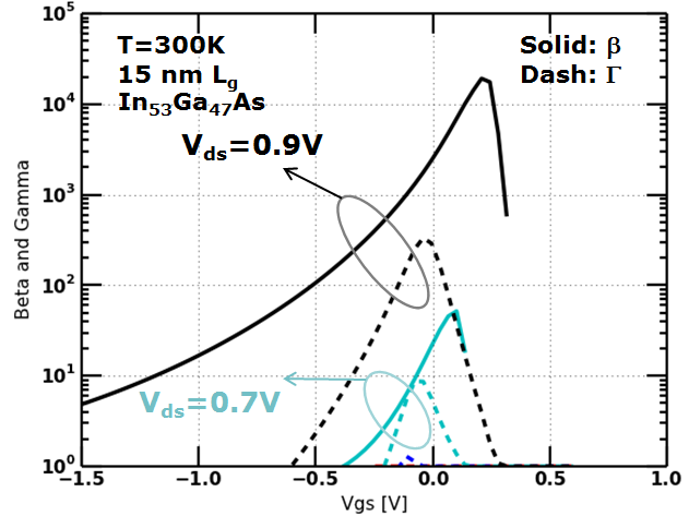
As can be seen in Fig. 12, bipolar gain is quite large, easily reaching into the thousands at high VDS. At low VDS, is negligible as expected, simply due to the fact that BTBT-driven hole generation is too low for any significant accumulation in the channel. The VGS behavior of is non-monotonic. At high VGS values, the source-channel barrier is reduced or suppressed entirely and holes can escape from the channel into the source. Thus, the steady-state hole concentration is low. At very negative VGS the feedback between IBTBT and the barrier height is pinning ID to a nearly constant value, suppressing further bipolar gain. In the intermediate region near the OFF-state of the transistor, bipolar gain is near maximum. The leakage penalty gain likewise peaks near the target OFF-state, albeit at lower values than . At high VDS, the true leakage penalty induced by PBE is seen to be approximately 100. Of course, this value is very device-structure specific. It can also be seen from Fig. 12 that is actually less than unity for strongly negative VGS, which is another way of saying that the leakage current in the presence of PBE is lower than it would have been without PBE. This is also a consequence of the pinned value of BTBT current in the presence of PBE (pinned when operating at strongly negative VGS). The relatively flat leakage tail in the presence of PBE is necessarily lower than the ’GIDL checkmark’ at sufficiently negative VGS. However, this should not be interpreted to mean that PBE is preferable to PBE-free operation; leakage in the standard operating regions of VGS is significantly worse in the presence of PBE (as shown in Fig. 12).
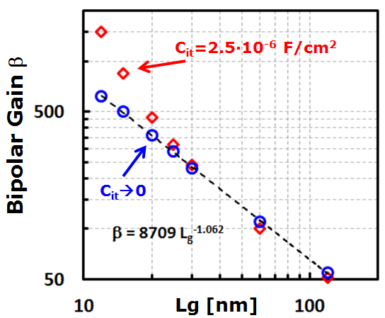
It was previously mentioned that gate electrostatics play a key role in determining the bipolar gain. Based on the capacitive voltage division suggested by Fig. 7, it is clear that control of the surface potential at the ToB is easily asserted by the ’deep’ channel potential via Cch if Cit is large compared to Cox. This coupling is a DIBL-like effect. Instead of remote positive charge in the drain influencing the ToB potential (which of course still takes place), there is a barrier lowering effect of the much more closely placed hole charge. Due to the proximity of the hole charge, the effective coupling capacitance of the holes to the ToB is larger than would be used to model the DIBL effect. We should therefore expect an electrostatics-induced departure from the usual scaling of bipolar gain when channel lengths approach the electrostatic limit imposed by the capacitive coupling to hole charge. This is the case of the measured In70Ga described in the first section of the paper, in which even a moderately long-channel device (120 nm) is experiencing significant PBE. In Fig. 13, this effect is illustrated by examining the Lg-dependence of for two cases: with and without Cit. The case of no Cit capacitor (i.e. C) has the best electrostatics possible within the geometry of the FinFET-on-insulator. Bipolar gain is seen to scale very nearly with the expected inverse-Lg law (as reported in [6] and [7]). However, the finite Cit case shows strong deviation from the inverse-Lg law below 30 nm Lg. As suggested by Fig. 7, the presence of a large Cit reduces the coupling of the surface potential at the ToB to the gate, diminishing the SCE performance in general, but more specifically allowing the ToB potential to be more closely controlled by the deep channel potential. This makes the source-channel barrier more susceptible to potential modulation by the injected hole charge, resulting in increased PBE gain. It should therefore be expected that FETs operating near the edge of Vt-rolloff (i.e. advanced CMOS devices pushed to the limit of Lg scaling). will have higher bipolar gains than would have been predicted based on inverse-Lg scaling alone.
V Impact of Substrate Architecture
In the previous sections it has been argued that the rate at which BTBT-generated holes can be extracted from the InGaAs channel is a key determinant of the magnitude of PBE gain, and thereby the OFF-state leakage. In this section, the choice of substrate architecture is shown to be critical importance in controlling PBE. The standard architectures usually considered for advanced nodes fall into several categories:
-
1.
FinFET on semiconductor substrate (’bulk’ substrate)
-
2.
FinFET on insulating substrate
-
3.
GAA configuration, such as a NW or Nanosheet (’wide NW’)
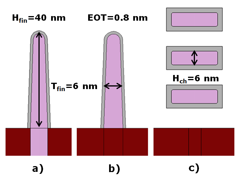
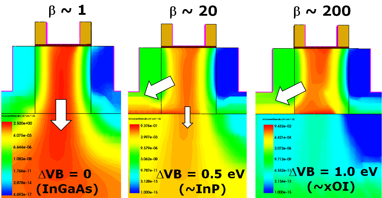
Of the three choices listed, only the ‘FinFET on semiconductor‘ choice provides a conductive path to the substrate. However, even in the case of the bulk substrate, the hole extraction path may be partially blocked by an energy barrier. The barrier is a consequence of the valence band (VB) mismatch (denoted as VB) between the channel material (in this case In53Ga47As) and the substrate material. Common choices for the substrate include InP and In52Al48As, both of which are lattice-matched to In53Ga47As. The former has a VB offset of approximately 0.5 eV relative to In53Ga47As, while the latter has an offset of 0.3 eV. Both are multiple kT at room temperature, and unless the channel/substrate interface is degenerately doped to enable channel-substrate tunneling, both barriers are expected to contribute to PBE. This is illustrated by simulation in Fig. 15. As seen in Fig. 15, channels with matched substrates (VB=0) have a direct path for minority holes to move into the substrate. No increase in channel potential is required, and the bipolar gain (shown at VDS=0.7V) is negligible. As the barrier height is increased to 0.5 eV (InP) or higher (approximating an insulating substrate), the hole current path through the substrate is suppressed. Bipolar gains even at low VDS are in the hundreds. The complete Id-Vg characteristics of devices with various substrates are shown in Fig. 16.
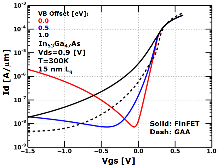
As illustrated in Fig. 16, increased barrier height results in the typical PBE-induced increase of sub-threshold slope, and generally higher leakage across most of the OFF-regime. Even with an InP substrate (VB=0.5 eV) the degradation in sub-threshold characteristics is noticeable. Deep in the accumulation region, leakage with strong PBE is actually lower than that of the no-PBE case (due to feedback-induced suppression of BTBT). However, in the normal operating regime for CMOS circuits, the high-barrier (and therefore high PBE) cases exhibit significantly higher leakage than the matched substrate case. This is further highlighted by the bipolar gains metrics shown in Fig. 17.
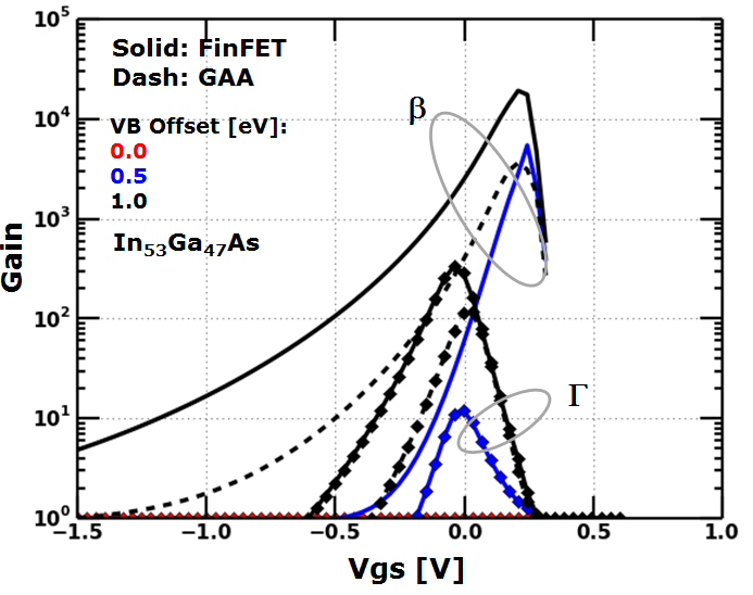
The bipolar gains and shown in Fig. 17 both show the strong effect of the substrate barrier. Bipolar gains with the InP substrate are in the hundreds (near the nominal OFF condition, with VDS=0.9V), while the true leakage penalty is about 10. The FinFET-on-insulator device has a leakage penalty of several hundred. In both Fig. 16 and 17, it is apparent that the GAA Nanosheet device has lower gains (both and ) than the corresponding FinFET-on-insulator, in spite of having no extraction path for holes (just like the FinFET-on-insulator case). This is a consequence of the somewhat improved electrostatics of the GAA device, relative to the bulk FinFET. The source-channel barrier of the GAA case is less perturbed by an increased channel potential (increased due to the presence of BTBT-induced holes), resulting in a smaller PBE gain. Referring to Fig. 7, the ratio of the series combination of Cox and Cit to Cch is better in the GAA FET than in the Fin-on-insulator FET.
It should be noted that the electrostatic benefit of a 20 nm wide GAA nanosheet over a FinFET is quite modest (much better improvement is available with a full NW structure, but this is not considered here), and the immunity to PBE is only slightly improved. It can therefore be concluded that a GAA device in the 15nm Lg range has a leakage penalty on the order of 100X relative to a true bulk FinFET (at the overdrive VDS voltage of 0.9V). This is certainly the case with the In70Ga30As GAA NW FETs of Fig. 3. Even though the device appears to be quite long on the electrostatic length scale, a large Cit due to interface traps (high Dit) reduces the coupling of the gate to the top of the barrier. In addition to standard SCE degradation, this degraded coupling is also making the device much more susceptible to PBE.
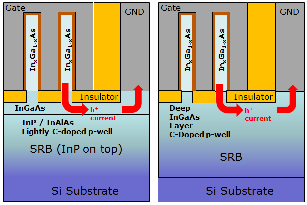
As shown in Figs. 17, all architectures other than FinFETs on zero-VB-offset substrates exhibit a leakage penalty, particularly under overdrive conditions. The only obvious solution to the PBE problem (short of using a large-bandgap channel material to suppress BTBT) is the FinFET with a substrate architecture shown in Fig. 18. Two flavors are illustrated, but both have two common features: the material directly under the fins (well top) exactly matches the channel, and a (remote) contact is placed in the well top. This ensures that a conductive path for hole extraction exists, with no barrier that would result in a charge pileup in potential shifts. The well top is the final layer of a thick SRB, which may include a wide-bandgap material as a subfin-leakage suppressor (or not, in which case doping is used for subfin leakage suppression). This is in fact very similar to the standard well contact scheme used for Si. It is a consequence of the high OFF-state leakage of narrow-bandgap materials that this may in fact be the only architecture possible for a low-power mobile SOC. For all its benefits, full GAA with a narrow bandgap material has a seemingly incurable PBE problem.
VI Summary and Conclusion
This paper presents evidence of strong PBE gains in GAA devices that utilize narrow-bangdap InGaAs. Measured data of moderate-length GAA devices exhibit a high level of leakage not consistent with BTBT alone. Furthermore, the VDS and VGS dependence of the leakage tails is not consistent with either pure BTBT leakage or punchthrough, but is well explained by PBE in conjunction with BTBT (through simulation), both at room and low temperature. Some aspects of the physics of PBE are elucidated upon. In particular, the dual-feedback mechanism which is responsible for the flattening of the Id-Vg curves in the OFF-state of devices with strong PBE is explained. It is also emphasized that this flattening is much more detrimental to FET behavior than the usual BTBT leakage. While the latter sets a leakage floor, PBE in conjunction with BTBT increases the sub-threshold slope in the near-OFF regime (the tail is not exponential, but has an increasing ‘local‘ SS as the device is pushed further toward the OFF state). It is argued that this behavior is fundamental to GAA FETs, due to the absence of a conductive path between the channel body and the substrate. Low-bandgap materials such as In53Ga47As (simulated in paper) or In70Ga30As (data and simulation in paper) are therefore not suitable for low-power SoC applications if GAA architectures are to be employed. Similar conclusions apply to FinFET-on-insulator architectures, since conductive coupling between the channel and the substrate does not exists. Even the case of the FinFET on semiconductor substrate is potentially problematic. The standard approach of using a wide-bandgap semiconductor (such as InP or InAlAs) as the substrate for InGaAs FinFETs is also found to lead to PBE gain, albeit more moderate than the GAA or the xOI case. The cause of the PB effect in this case is the valence band offset between the InGaAs channel and the InP (or InAlAs) substrate. This offset presents a barrier for holes, resulting in hole accumulation in the channel (i.e. the standard PBE mechanism). The only substrate option which eliminates PBE is found to be one in which the channel and the substrate material are matched (or at least their valence band edges are aligned) and a well contact is placed into the matched well material (possibly in a remote cell which shares the substrate material). Thus, it would appear that a bulk FinFET architecture is preferable to GAA for low-leakage InGaAs devices.
References
- [1] M. Radosavljevic, B. Chu-Kung, S. Corcoran, G. Dewey, M. K.Hudait, J. M.Fastenau, J. Kavalieros, W. K.Liu, D. Lubyshev, M. Metz, K. Millard, N. Mukherjee, W. Rachmady, U. Shah, and R. Chau , ”Advanced high-K gate dielectric for high-performance shortchannel In0.7Ga0.3As quantum well field effect tran-sistors on silicon substrate for low power logic applications”, Proc. IEEE IEDM, Dec. 2009
- [2] S. Lee, C.-Y. Huang, D.C. Elias1, B.J. Thibeault, W. Mitchell, V. Chobpattana, S. Stemmer, A.C. Gossard, and M. Rodwell, ”35 nm- Lg Raised S/D In0.53Ga0.47As Quantum-well MOSFETs with 81 mV/decade Subthreshold Swing at VDS=0.5 V”, 2014 72nd Annual Device Research Conference, DRC 2014
- [3] N. Waldron, S. Sioncke, J. Franco, L. Nyns, A. Vais, X. Zhou, H. C.Lin, G. Boccardi, J. W.Maes, Q. Xie, M. Givens, F. Tang, X. Jiang, E. Chiu, A. Opdebeeck, C. Merckling, F. Sebaai, D.van Dorp, L. Teugels, A. S.Hernandez, K.De Meyer, K. Barla, N. Collaert. Y-V. Thean ”Gate-All-Around InGaAs Nanowire FETS with Peak Transconductance of 2200μS/μm at 50nm Lg using a Replacement Fin RMG Flow”, Proc. IEEE IEDM, Dec. 2015
- [4] T. Rakshit, B. Obradovic, W. -E. Wang, W. -H. Kim, K. -M. Shin, S. -C. Baek, S. -W. Lee, S. -H. Kim, J. -M. Lee, D. Kim, A. Hoover, W.-B. Song, M. Cantoro, Y.-C. Heo, R. Rooyackers, S. C. Ardila, A. Vais, D. Lin, N. Collaert, and M. S. Rodder, ”A New Direction for IIIV FETs for Mobile CPU Operation Including Burst-Mode: In0.35Ga0.65As Channel”, IEEE Electron Device Letters, Vol. 38, No. 3, March 2017
- [5] F. Liu, I. Ionica, M. Bawedin, S. Cristoloveanu, ”Effect of back gate on parasitic bipolar effect in FD SOI MOSFETs”, SOI-3D-Subthreshold Microelectronics Technology Unified Conference, 2014 IEEE
- [6] J. Lin, D. A. Antoniadis, and J. A. del Alamo, ”Off-state leakage induced by band-to-band tunneling and floating-body bipolar effect in InGaAs quantum-well MOSFETs”, IEEE Electron Device Letters, Vol. 35, No. 12, Dec. 2014
- [7] J. Lin D. A. Antoniadis and J. A del Alamo, ”Physics and Mitigation of Excess OFF-State Current in InGaAs Quantum-Well MOSFETs”, IEEE Transactions on Electron Devices, Vol. 62, No. 5, May 2015
- [8] Sentaurus Device User Guide, Synopsys Inc., 2016.
- [9] Q. Smets, D. Verreck, A.S. Verhulst, R. Rooyackers, C. Merckling, M. D.Put, E. Simoen, W. Vandervorst, N. Collaert, V Y.Thean, B. Soree, G. Groeseneken, and M. M.Heyns ”InGaAs tunnel diodes for the calibration of semi-classical and quantum mechanical band-to-band tunneling models”, Journal of Applied Physics, Vol. 115, 184503, 2014
- [10] G. Klimeck, R. Bowen, T. Cwik, and T. Boykin, ”sp3s* and sp3d5s* tight-binding parameter sets for GaAs, AlAs, InAs, GaSb, AlSb, InSb, GaP, AlP, and InP for quantum dot simulations”, Proc. March Meeting Amer. Phys. Soc., Minneapolis, MN, USA, Mar. 2000