Quasiperiodic ordering in thick Sn layer on -Al-Pd-Mn: A possible quasicrystalline clathrate
Abstract
Realization of an elemental solid-state quasicrystal has remained a distant dream so far in spite of extensive work in this direction for almost two decades. In the present work, we report the discovery of quasiperiodic ordering in a thick layer of elemental Sn grown on icosahedral ()-Al-Pd-Mn. The scanning tunneling microscopy (STM) images and the low energy electron diffraction patterns of the Sn layer show specific structural signatures that portray quasiperiodicity but are distinct from the substrate. Photoemission spectroscopy reveals the existence of the pseudogap around the Fermi energy up to the maximal Sn thickness. The structure of the Sn layer is modeled as a novel form of quasicrystalline clathrate on the basis of multiple supporting evidences: Firstly, from ab-initio total energy evaluation, the energy of bulk Sn clathrate quasicrystal is lower than the high temperature metallic -Sn phase, but higher than the low temperature -Sn phase. A comparative study of the free slab energetics shows that surface energy favors clathrate over -Sn up to about 4 nm layer thickness, and matches -Sn for narrow window of slab thickness of 2-3 nm. Secondly, the bulk clathrate exhibits gap opening near Fermi energy, while the free slab form exhibits a pronouced pseudogap, which explains the pseudogap observed in photoemission. Thirdly, the STM images exhibit good agreement with clathrate model. Finally, we establish the adlayer-substrate compatibility based on very similar (within 1%) the cage-cage separation in the Sn clathrate and the pseudo-Mackay cluster-cluster separation on the -Al-Pd-Mn surface. Furthermore, the nucleation centers of the Sn adlayer on the substrate are identified and these are shown to be a valid part of the Sn clathrate structure. Thus, based on both experimental and ab-initio density functional theory calculations, we propose that 4 nm thick Sn adlayer deposited on 5-fold surface of -Al-Pd-Mn substrate is in fact a metastable realization of elemental, clathrate family quasicrystal.
I Introduction
The mathematical concept of aperiodic ordering and the discovery of quasicrystals brought paradigm shift in crystallographyShechtman_prl84 ; Penrose74 . Quasiperiodicity has been observed in naturally occurring mineralsBindi09 , different inter metallic compoundsTsai00 , binary nano-particle super latticesTalapin09 colloidal quasicrystalFischer11 , oxide thin filmForster13 and large molecular assembliesXiao12 ; Ye16 . A recent exciting finding is the nontrivial topological property of quasiperiodic systemsKraus16 ; Zhou19 . The technological importance of quasicrystals arise from their low frictional coefficient, heat insulation and photonic band gapPark05 ; Dubois12 .
However, the chemical complexity of quasicrystals discovered so far hinders their applicability and basic understanding of their unusual properties. An elemental quasicrystal would be best suited for this purpose, but a single-element bulk quasicrystal has not been yet observed. Efforts in this direction for over a decade have involved the use of quasicrystalline substrates as a template to grow quasiperiodic elemental layersFranke_prl02 ; Shimoda_jns04 ; Sharma_prb05 ; Krajci_Snprb05 ; Shukla_prb06 ; Ledieu_prb08 ; Smerdon_prb08 ; LedieuPbAPMprb09 ; Sharma_prb08 ; Shukla_prb09 ; Krajci_PbAPM_prb10 ; Sharma13 ; Hars_ss18 . Pseudomorphic growth of one monolayer (ML) quasiperiodic Sn has been reported in the past on decagonal ()-Al-Ni-CoShimoda_jns04 and icosahedral ()-Al-Cu-FeSharma_prb05 . A density functional theory (DFT) study predicted pseudomorphic growth of quasiperiodic Sn on -Al-Pd-MnKrajci_Snprb05 . In most of the studies in the past, only the first wetting layer has been reported to exhibit five-fold quasiperiodicity with a structure similar to the substrate. Pb/-Ag-In-Yb showed five-fold growth isostructural with the substrate and pentagonal motifs with maximum height of about 0.7 nm were identifiedSharma13 . It may be noted that although the thickness was substantial, five-fold quasiperiodicity was not observed in 25 ML Cu/-Al-Pd-MnLedieu_prl04 or in 1.8 nm thick Ag on GaAsSmith , rather aperiodic modulation of row separation were observed only in one direction.
It is interesting to note that elements from group XIV of the periodic table have specific propensity to form pentagonal or even icosahedral structures. Although Sn exhibits a diamond type structure (-Sn, space group Fdm) at low temperature and a tetragonal structure (-Sn, space group I41/amd) above 286 K, it is well known that Sn can form -bonded clathrate structures whose canonical constituents are four kinds of cages that are bounded exclusively by pentagonal and hexagonal faces. Out of the four canonical cages, the most abundant one in common clathrate crystals is the dodecahedral cage with icosahedral symmetry, bounded exclusively by 20 pentagonal faces, in contrast to purely hexagonal diamond structure (see Fig.5 in Section III.D). Intriguingly, in their computer simulation Engel et al.qcla observed spontaneous formation of three icosahedral phases, and the “loosely packed” phase can be regarded as an imperfect realization of the icosahedral quasicrystal clathrate. Last but not the least, the dodecahedron cage found in clathrates is identical with the second shell of the so called mini-Bergman clusters, playing fundamental role in -Al-Pd-Mn structure.
In this work, we observed that Sn deposited on -Al-Pd-Mn surface retains quasiperiodic ordering up to maximal achievable coverage leading to nearly 4 nm thickness, indicating the existence of the first intrinsic - although apparently metastable - monoatomic realization of a quasicrystal. We model it as a quasicrystal structure belonging to the clathrate family strictly maintaining tetrahedral coordination consistent with bonding. We justify plausibility of the model by energetic considerations within the DFT framework, based on the structural comparison with experimentally observed motifs, and from the character of electronic density of states (DOS) near Fermi energy.
II Methods
The single grain fivefold -Al-Pd-Mn quasicrystal surface was prepared by repeated cycles of Ar+ ions sputtering and annealing to about 900-930 K for 22.5 h. The cycles were repeated until sharp fivefold low energy electron diffraction (LEED) pattern was observed. Sn (99.99% purity) was evaporated from a water cooled Knudsen evaporation cellShukla_rsi04 . The evaporation cell was operated in the temperature range of 10731163 K at a pressure of 210-10 mbar during the deposition. For the thick layer growth, we used an effective deposition rate of 0.06 to 0.4 ML/min in repeated cycles of 1 min deposition followed by 1 min waiting time. Sn deposition was carried out with the substrate close to room temperature (RT 300- 330 K) and at 150 K. The temperature of the substrate was measured using a K-type thermocouple.
The STM measurements were carried out at a base pressure of 210-11 mbar using a variable temperature STM from Omicron GmbH. STM measurements were performed at room temperature (RT) and 80 K in the constant current mode using a tungsten tip that was cleaned by field emission, sputtering and voltage pulse method. The tip was biased and the sample was kept at the ground potential. It may be noted that same kind of tiles and motifs are observed for different bias voltages ranging from -2.6 to 2.8 V for different coverages, which demonstrate that the features are topography related. The zero in the vertical scale of a STM image is set at the bearing height, which is the most dominant height value, based on a height distribution histogram. LEED was performed using 4-grid rear view optics from OCI Vacuum Microengineering.
The ultraviolet photoemission spectroscopy (UPS) measurements at 150 K were performed using R4000 electron energy analyzer with wide angle lens using 21.2 eV photon energy incident at 45∘ with respect to () the surface normal and measured in normal emission, with an analyzer acceptance angle of 15∘ in transmission mode and a resolution of 50 meV. The Fermi edge was measured on a metallic sample in electrical contact with the specimen. X-ray photoelectron spectroscopy (XPS) measurements were performed with 1253.6 eV (MgK) photon energy with a resolution of 0.8 eV using Phoibos 100 electron energy analyzer. The thickness of the Sn adlayer has been determined by STM and also by XPS from the intensities of Sn 3 and Al 2 core level peaks using the well known relations = (1- exp(-/ cos)) and = exp(-/ cos) where is the thickness, is the emission angle= 55∘ and is the mean free path. for Sn 3 (14.2Å ) and Al 2 (19.6Å) are consistent with Ref. TPP2M, .
The DFT calculations have been carried out using the Vienna Simulation Package (VASP)VASP1 by performing an iterative solution of the Kohn–Sham equations of DFT within a plane wave basis. We use projector augmented wave potentialsPAW in the PW91 generalized gradient approximationPW91 . For both bulk and free slab structures, cohesive energies are converged to less than 1 meV/atom with basis set containing plane waves with a kinetic energy up to = 150 eV. The self-consistency iteration were stopped when total energies are converged to within 10-6 eV. All the structures, bulk models as well as slabs, were fully relaxed without constraints, and including the cell parameters. -point meshes have been converged to satisfy for each mesh dimension 100, where are edges of the periodic cell.
III RESULTS AND DISCUSSION
III.1 STM and LEED of monolayer Sn on -Al-Pd-Mn
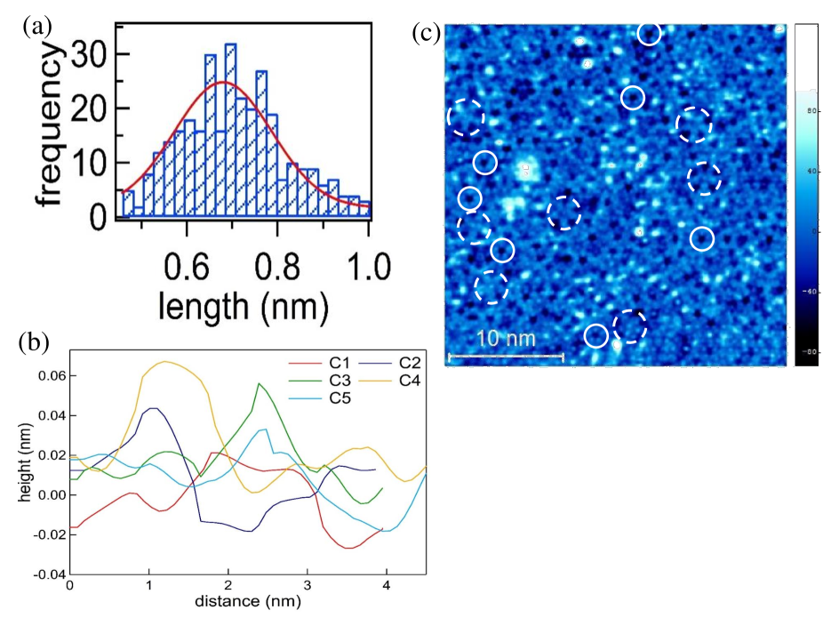
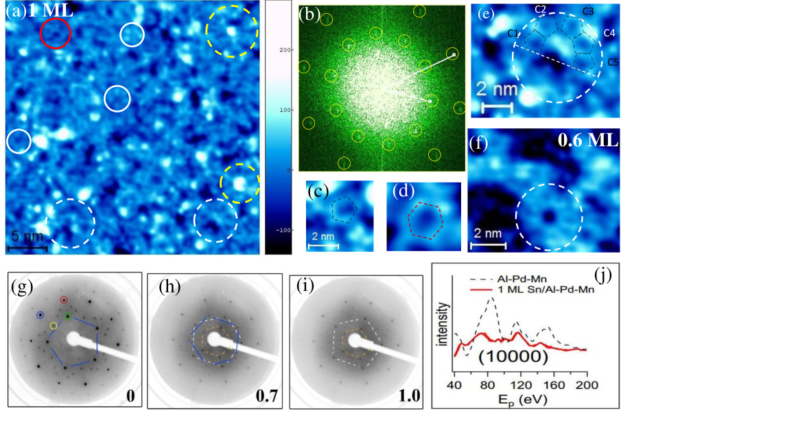
We begin our discussion by a high resolution STM image of 1 ML Sn/-Al-Pd-Mn in Fig. 1(a). It is clearly quasiperiodic, as demonstrated by its Fourier transform (FT) that exhibits two sets of spots of tenfold symmetry highlighted by yellow circles [Fig. 1(b)], whose distance from the center (white lines) is in the ratio of , where is the golden mean ( 1.618). The most prevalent tile in the Sn layer is a pentagon with a central dark region [Fig. 1(c)], as shown by black dashed lines. The length of the sides of these pentagonal ()-tiles is around 0.7 nm, as shown by its length distribution in Fig. S1(a) of the Supplementary Material (SM)supplement . Hexagonal tiles, although rare, are also observed with length scale similar to the -tiles [Fig. 1(d)]. The different motifs formed by the congregation of such tiles are highlighted by circles in Fig. 1(a). A distinctive motif of the Sn layer that is not observed for -Al-Pd-Mn is a circular congregation having common sides that we refer to as wheel motif (yellow dashed circles), while half-circular or incomplete wheel motif is named as crown motif (white dashed circle). An expanded view of a crown motif, seen in the bottom right corner of Fig. 1(a), is shown in Fig. 1(e). It shows five tiles (C1 to C5) clearly not in the same plane forming a half circle. Noteworthy is that the height profiles (Fig. S1(b) of SMsupplement ) along the sides of these tiles show the maximum puckering to be about 0.06 nm, which is sizeable compared to the thickness of the 1st layer (0.26 nm). The puckered nature of the Sn layer can also be quantified by the root mean square roughness (), which turns out to be 0.04 nm, which is twice that of -Al-Pd-Mn (= 0.02 nm). A hexagonal tile centered motif in red circle in the top left side of Fig. 1(a) also indicates that the tiles are not in the same plane. It is noteworthy that even in the submonolayer regime, for example at 0.6 ML, as the Sn adatoms form islands, the crown motif is observed [white dashed circle in Fig. 1(f)]. In contrast to the -tiles that are uniform, pentagons with bright vertices with side length of about 1.1 nm are occasionally observed [white circles in Fig. 1(a)]. These are different from the white flowers of -Al-Pd-Mn because here a central dark region is observed.
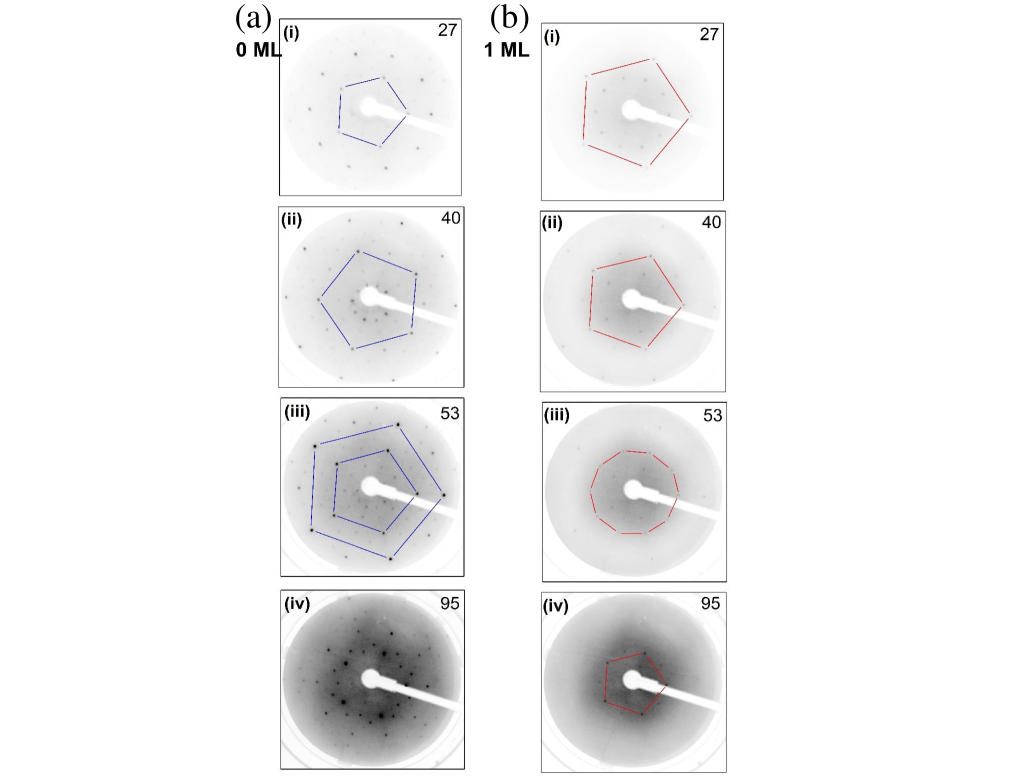
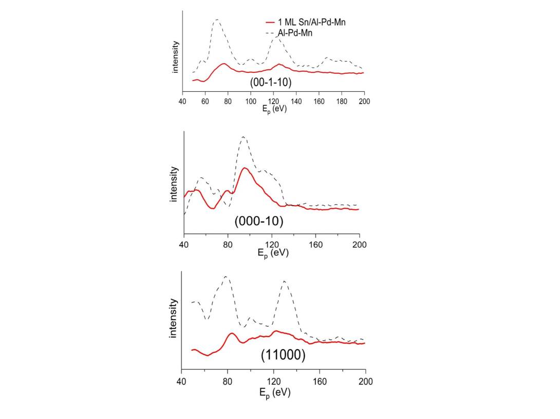
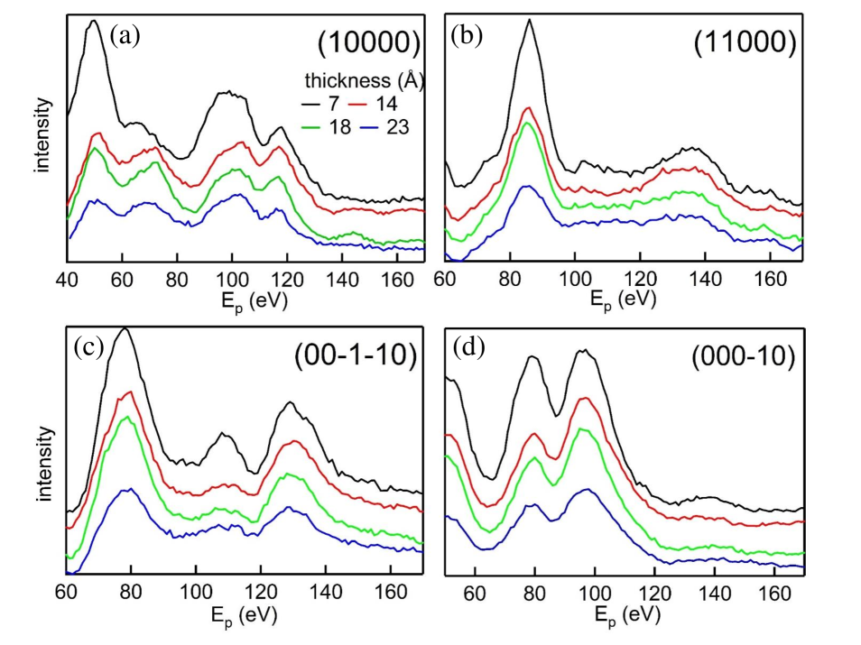
The LEED of the Sn monolayer is distinctly different from the substrate: the latter recorded with beam energy () of 81 eV exhibits two sets of ten spots, inner and outer [Fig. 1(g)], in agreement with literatureGierer_prl97 ; Barbier02 . A blue pentagon connects the intense (10000) spots of the inner set, while (000) and (11000) spots on the outer set are also indicated by circles. As Sn coverage increases, the intensities of (0000) spots increase (white dashed pentagon) whereas in contrast the (10000) intensities decrease (blue pentagon) [Fig. 1(h)]. Furthermore, a set of five innermost spots appears forming a smaller pentagon (yellow dashed) with an orientation rotated ∘ the blue pentagon. In the LEED pattern for 1 ML Sn in Fig. 1(i), the spots joined by white and yellow dashed pentagons remain clearly visible, while the (10000) spots become inconspicuous. At other too, the LEED pattern is modified (Fig. S2 of SMsupplement ). Consequently, the intensity versus beam energy (IV) curves for (10000) in Fig. 1(j) (as well as for (0000), (00 0) and (11000) spots in Fig. S3 of SMsupplement ) are different between the Sn monolayer and -Al-Pd-Mn, demonstrating the structural differences between the two.
III.2 STM and LEED of Sn multilayers
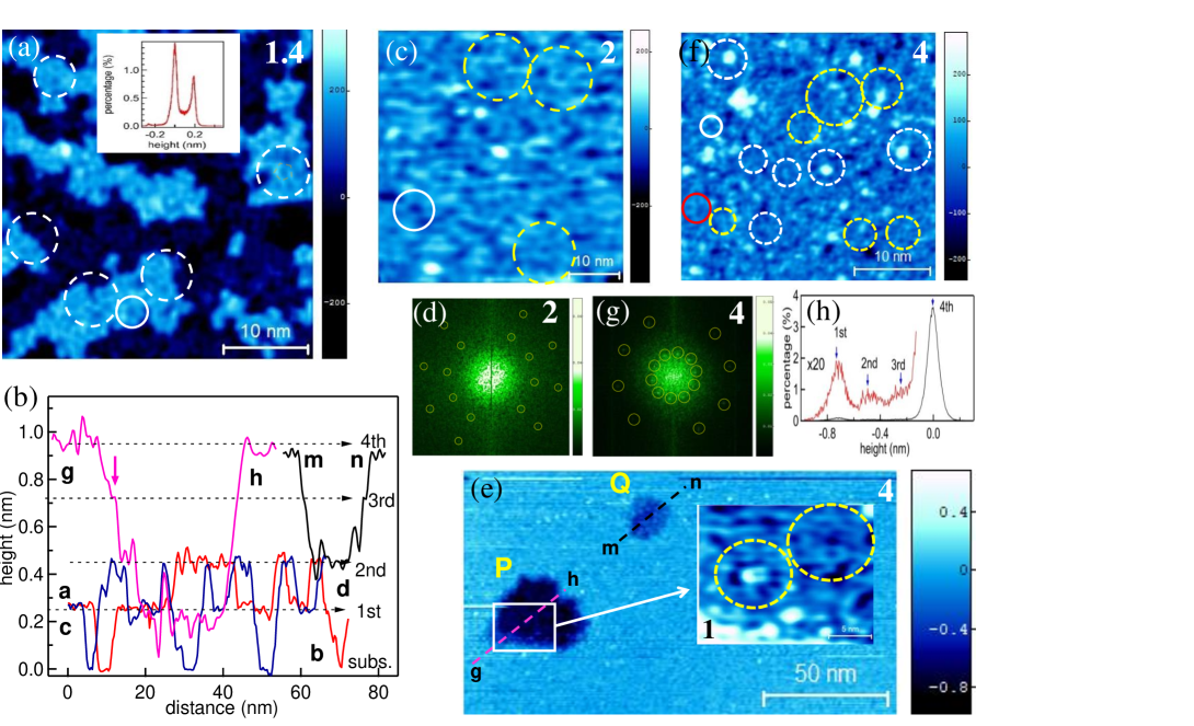
The growth of the 2nd layer is initiated by formation of condensed islands, as shown in the STM image for 1.4 ML Sn/-Al-Pd-Mn [Fig. 2(a)]. The height distribution histogram [inset, Fig. 2(a)] and the height profiles given in Fig. 2(b) along and in an extended area image in Fig. S4supplement show that all the islands representing the second layer are 0.2 nm thick indicating layered growth. This is expectedBauer58 because the surface energy of Sn (0.71 )Tyson77 ; Vitos98 is less than that of -Al-Pd-Mn (0.82 )Dubois06 . Fig. 2(c) shows the fully formed 2nd layer, and the motifs are highlighted by circles. The quasiperiodicity is confirmed by the FT [Fig. 2(d)] that shows two sets of spots (yellow circles) with tenfold symmetry, whose distance from the center is in ratio of . The motifs are similar to the monolayer of Sn discussed in the previous section. The wheel (yellow dashed circle) and pentagon with bright vertices (white circle) are observed. The second layer is also puckered with = 0.05 nm.
In order to enhance the thickness, we have deposited Sn at a lower temperature (150 K) since it is very difficult to grow thicker layers at RT despite longer time deposition because of low sticking rate of Sn. The occurrence of 4th layer is established by analyzing the pit P in lower left corner of Fig. 2(e). The inset is the expanded image of the floor of P that is enclosed by white rectangle. It shows Sn motifs similar to a Sn layer and hence it is at least 1 ML thick. Thus, the three weak peaks in the height distribution histogram [Fig. 2(h)] can be assigned to the 1st (floor of the pit P), 2nd (floor of the pit Q), and 3rd layer (at edges of pits P and Q), while the main peak corresponds to the 4th layer. The height profiles along lines and in Fig. 2(b) also show this, the transition from 3rd to 4th layer is shown by a change in slope (pink arrow). In fact, the pink height profile along shows formation of three Sn layers of nearly equal heights. This is incompatible with the quasiperiodic step heights of the -Al-Pd-Mn substrate, hence confirming the growth of four Sn layers.
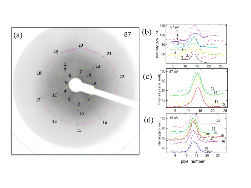
A high resolution STM image for the 4th layer in Fig. 2f show the wheel, crown (dashed circles), and the triplet motifs (red circle) that are similar to the thinner layers. FT corresponding to the 4th layer [Fig. 2(f)] exhibits two set of spots [Fig. 2(g)], whose distance from the center is in the ratio of 1:. The LEED patterns exhibit five fold symmetry within the coherence length scale of the instrument (Fig. S5supplement ). It shows three sets of sharp spots comprising of an inner set of 9 spots forming a decagon (connected by yellow lines, the 10th spot is hidden by the shadow of the electron gun), 4 intermediate spots forming a pentagon (green dashed lines) and 9 outer spots (dashed pink lines). Intensity profiles through each of the spots are also shown in Fig. S5. Quasiperiodicity is reasserted by the distances of the innermost, inner and outer set of spots from (0, 0) in ratio 1:1.63:2.7 1::. Here, it is worth mentioning that in contrast to the present results, Sn grown on -Al-Cu-Fe showed island growth after the 1st quasiperiodic layerSharma_prb05 possibly because in that work the deposition was done at much higher temperatures (573-623 K) and large deposition rate of 15 ML/min, where activated diffusion of Sn across terraces might have resulted in clustering and island growth. In contrast, our deposition temperature for growing thicker layers is 150 K and the deposition rate is much lower (see section II).
III.3 Thick Sn layer studied by STM and LEED
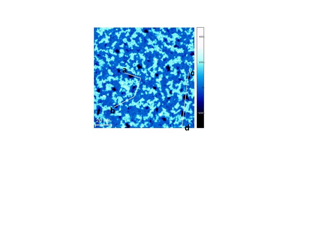
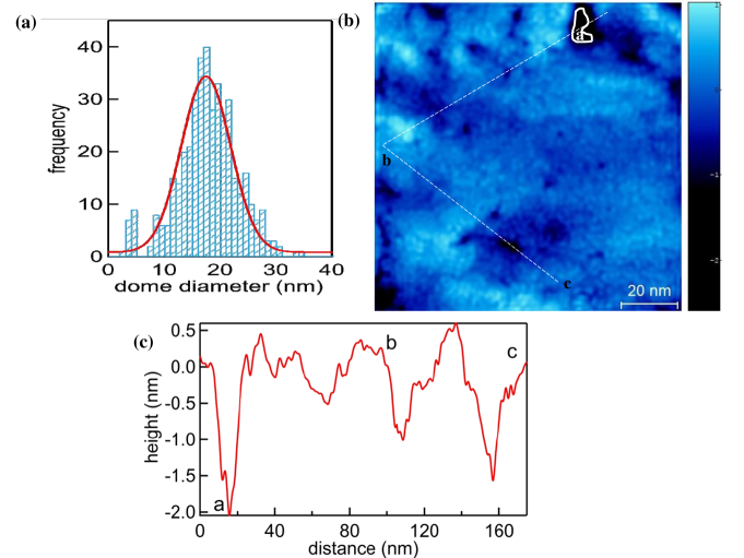
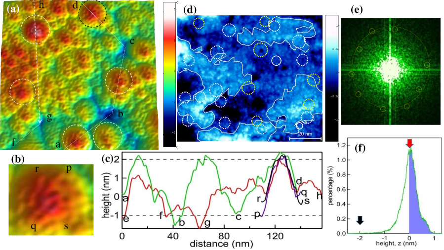
In order to obtain quasiperiodic Sn of even larger thickness, the deposition was done at 150 K for twice the time compared to the previous (4th layer) deposition and the layer was cooled down to 80 K. In this case, the STM image in Fig. 3(a) shows dome-like structures of uniform shape with a circular base (highlighted by dashed circles). Interestingly, an expanded view of a dome in Fig. 3(b) shows a central pentagonal tile surrounded by other pentagonal tiles forming a network. The maximum height of these domes is 3 nm from the base, as shown from the height profiles [Fig. 3(c)] along and of Fig. 3(b) and along and of Fig. 3(a). The diameter of the base of the domes exhibits a Gaussian distribution centered at 17.5 nm with a FWHM of about 10 nm, as shown in Fig. S6(a)supplement . The puckered nature of the surface is increased by a large amount as portrayed by = 0.4 nm.
However, possibly due to a competition between three dimensional versus layered growth, the domes are not visible everywhere on the surface. For example, in Fig. 3(d), a different region shows relatively longer range undulations of 50 nm (see also Figs. S6(b) and S6(c)supplement for an extended area image and height profile). It is relatively flat compared to Fig. 3(a) with smaller = 0.3 nm. Here, motifs such as wheel (yellow dashed circle), crown (white dashed circle), pentagon with bright vertices (white circle) are observed. Moreover, in Fig. 3(e), the ten fold FT confirms the quasiperiodic nature of the layer; a marginal deviation in the arrangement of these spots from circle could be because of finite amount of thermal drift during scanning.
In order to find the thickness of this layer, we note that the peak of the height histogram at = 0 nm (red arrow in Fig. 3f) shows that about 50% of the area (shaded with blue color) has a thickness (or height) of 2 nm the minimum at -2 nm (black arrow). The minimum region is identified to be around in Fig. S6(b) from the height profile shown in Fig. S6(c). Since we obtain a thickness of 1 nm for the wetting layer up to the 4th layer, an estimate of the thickness of the minimum region around in Fig. S6(b) is 1 nm. Thus, the thickness of the regions enclosed by white contour lines in Fig. 3(d) is 3 nm. Presence of many quasiperiodic motifs (encircled) in this region that are similar to the motifs observed in the 2-3 nm thick region outside the contour lines or those in Figs. 1, 2 indicates similar quasiperiodic structure in the 3 nm region. An estimate of the height of the Sn domes in Fig. 3(a), by the same argument discussed above, is 4 nm, since these are at a height of 3 nm from the base (Fig. 3(c)), and the base can be taken to be 1 nm in thickness. The appearance of domes and undulations [Fig. 3(a,d)] is indicative of transformation towards quasiperiodic ordering in the vertical direction, which could be expected as the Sn-adlayer becomes thicker. The growth transforms from puckered but primarily two dimensional to quasiperiodic growth in all three directions similar to a bulk quasicrystal. We find that the thick film is not stable when warmed up to RT, as is evident from 40-50% decrease of the Sn Auger signal, which is possibly caused by the Sn atoms diffusing out to the sides of the substrate. Diffusion of Sn from the back of Al-Ni-Co substrate to the front with increasing temperature has been reported in literatureShimoda_jns04 .
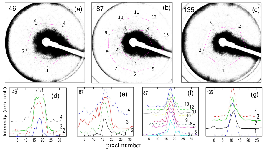
Further evidence of quasiperiodicity in this thick layer in the macroscopic length scale is provided by the LEED patterns that show sharp five fold spots [Fig. 4(a-c)]. The intensity profiles of each of the spots are shown in [Fig. 4(d-g)]. At 87 eV [Fig. 4(b)], the outer 10 spots and the inner pentagon are observed and the ratio of their distance from the (0,0) specular spot is 1:1.63 1:. At beam energies of 46 eV and 135 eV [Fig. 4(a,c)], four spots representing a pentagon are observed, the fifth spot is hidden by the shadow of the electron gun. In Fig. S7supplement , the IV curves for the thicker Sn layers are shown, their peak positions are similar to that of 1 ML Sn, indicating their structural similarity. LEED patterns as a function of beam energy are shown by the video files in SM, such as, 3nmleed for the 3 nm Sn layer, 1.8nmleed for 1.8 nm, 1nmleed for 1 nm and 0.25nmleed for the 0.25 nm (or 1 ML) Sn layer thicknesssupplement . If an adlayer has different domains, it results in the appearance of multiple spots in the LEED pattern. There are reports of such rotational epitaxy for different metals grown on -Al-Pd-MnSharma ; Bolliger . On the contrary, our LEED patterns (Figs. 1, 4, S2, S5 and the video files) show that all the spots move towards the (0,0) spot with increasing beam energy. Importantly, no extra spots appear or splitting of the spots occur over the whole beam energy range. We also do not observe any signature of spots arranged in a periodic fashion that is characteristic of crystalline or approximant phases. We however note that the thicker layers have disorder, as also corroborated by the theoretical clathrate model that is discussed later, which results in relative weakening of the LEED spots at larger thickness. But, what is very important is that all the LEED patterns show only quasiperiodic spots with no hint of any alternative ordering.
III.4 Quasicrystal clathrate model of Sn
The motifs observed from scanning tunneling microscopy as well as the low energy electron diffraction patterns show structural signatures for the Sn film that are distinct from the substrate. Sn thus exhibits intrinsic quasiperiodic growth to a thickness of 3-4 nm, which almost in the realm of bulk-like quasiperiodic growth where impact of the substrate becomes negligible. This is because the effective potential of a solid including the exchange interaction term perpendicular to the surface is almost zero beyond unity Fermi wavelengthLang70 . Al and Mn that form the top layer of -Al-Pd-Mn both have Fermi wavelengths of about 0.36 nm, which is almost an order of magnitude less than the 4 nm thickness of the quasiperiodic Sn layer. The function of the substrate is to suppress initial formation of stable crystalline forms of Sn the and -Sn.
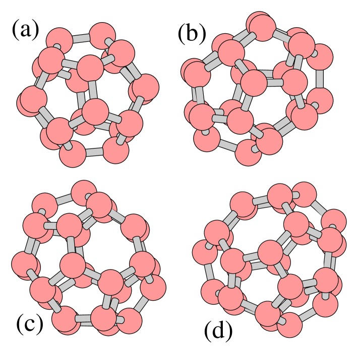
In the Sections III.D through III.I, we combine the geometrical concepts and DFT calculations, while in Section III.J, we discuss how Sn white flower (SnWF) cluster facilitates nucleation of the intrinsic Sn structure. We show that the intrinsic Sn structure is a metastable clathrate quasicrystal, and that in a narrow window of covering widths of 3-4 nm, an unsupported pentagonal clathrate structure is more stable compared to -Sn. In the -Sn structure, atoms are tetrahedrally coordinated and satisfy the type bonding scheme. But there exists a whole family of alternative structures – clathrates – satisfying the same tetrahedral bonding scheme (Fig.5), achieving that goal by grouping atoms around point centers into empty “cages”. Indeed “empty” clathrates are experimentally achievable metastable states of GeGuloy or SiGryko , and there is a broad family of clathrate structures that are stabilized by addition of large “host” atoms captured inside the cages. The clathrate structures are modular in the sense that the constituting polyhedral cages can be nontrivially recomposed into variety of periodic arrangements.
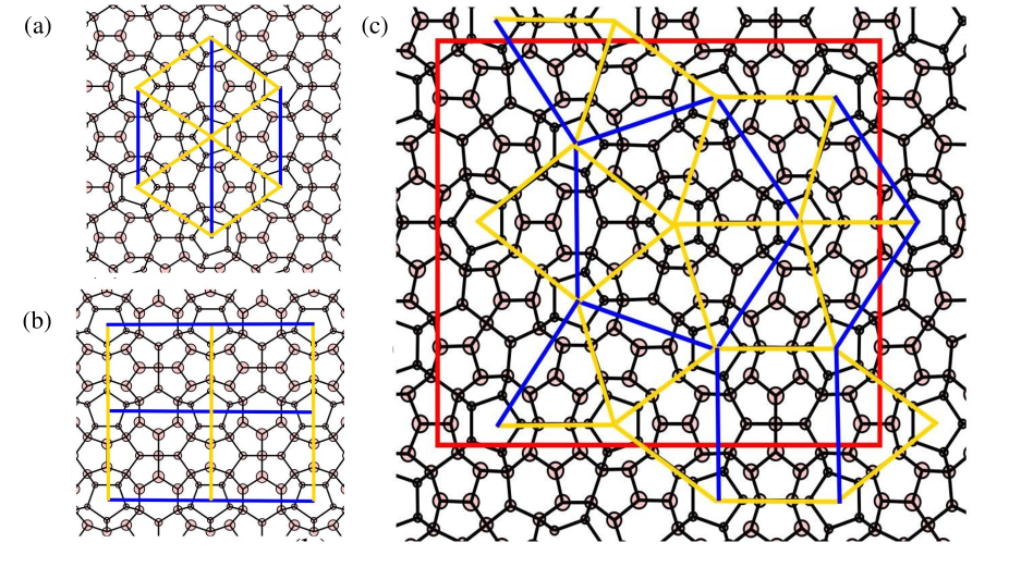
Two of the known clathrate structures commonly designated as type II and III exhibit special relationship, illustrated in Fig. 6(a,b) – they share a common pseudo 5-fold axis, and equal vertical periodic repeat that is about 12.7Å in case of Sn. Size of the circles representing the atoms scales with their vertical height, and the neighboring atoms are connected by black lines along 2.9Å long interatomic bonds. Associating the centers of the decagonal rings (decorated inside by pentagons) with the tiling vertices reveals the geometric backbone of the structures: tiling of isosceles triangles T with wider angle 72∘ (two yellow and the longer blue sides), and rectangles R with aspect ratio /; blue linkages denoted are about 12.6Å long, and the shorter yellow linkage is given by 10.82Å. Since the tile decoration is symmetric and identical for all the yellow edges in both structures, and the same holds for the blue linkages. The cage motifs from two prototype structures can be combined to form a family of variant structures that are in one-to-one correspondence with planar rectangle–triangle (R-T) tilings. The R-T tilings may be arranged periodically as in Fig. 6(c), but the local 5-fold axial symmetry of the cages eventually leads to global pentagonal order of the quasiperiodic structuresCOC . Thus the clathrate recipe for R-T tiling decoration gives rise to whole family of pentagonal structures, periodic, quasiperiodic or disordered.
We note that the cage-cage linkage length in Sn clathrates of 12.6Å almost exactly coincides (to within 1%) with the pseudo-Mackay cluster-cluster separations in -Al-Pd-Mn of 12.55Å (-times the intercluster linkages of 7.7Å between “mini-Bergman” or between “pseudo-Mackay icosahedra” clusters). In the clathrates, the prevalent dodecahedral cages have icosahedral symmetry, and sections through the cage normal to a 5–fold axis will have pentagonal symmetry. Since the symmetry of the LEED patterns [Fig. 4, Fig. S5] is determined by the surface layer, we predict that in general their symmetry will be 5-fold.
III.5 Quasicrystal clathrates as duals of the Frank-Kasper structures
In Frank–Kasper (FK) structures, the space is divided into face-sharing tetrahedra. Decorating each tetrahedron center by Sn atom, every tetrahedron’s face is intersected by a bond between pair of neighboring Sn atoms. Since there are four faces for every tetrahedron, every Sn atom is guaranteed to have four neighbors in the directions of the surrounding face centers. Thus, tetrahedrally close packed structures are in one to one correspondence with their dual, clathrate relativesFK ; FK59 ; OAS . Four canonical FK polyhedra with triangulated coordination shells – Z12, Z14, Z15 and Z16 – become respectively 20, 24, 26 and 28-vertex cages, whose faces are pentagons and hexagons. This dual relationship is an alternative path to the decagonal clathrates defined above, by dual-transforming decagonal FK structures. The two clathrates from Fig. 6(a, b) are in fact dual relatives of the FK prototypes Cu2Mg and Al3Zr4 FK structures. Moreover, we could generalize clathrates to include 12-fold dodecagonal quasicrystals based on FK decoration of square-triangle tilingsII , whose strictly quasiperiodic version would be based on Stampfli’s square-triangle inflation ruleZU .
The possibility of icosahedral FK structure whose dual would be perfect icosahedral clathrate is not clear. The only locally icosahedral and strictly tetrahedrally close-packed structure known is, to our knowledge, the “1/1” icosahedral approximant with prototypical natural realization in Al-Mg-Zn system, discovered by Bergman Bergman52 In their milestone paper, Henley and ElserHE described this structure as a simple decoration of Penrose rhombohedra, and proposed that generalization of that decoration scheme eventually leads to FK quasicrystal enjoying global icosahedral symmetry. But there is a bottleneck: the decoration rule requires that all “oblate” rhombuses in the 3D Penrose tiling are paired along their short body diagonals, but such tiling of 3D golden rhombuses is not known at present. An interesting aspect of the bulk icosahedral clathrate is its possible genuine entropic advantage over layered quasicrystals.
Relaxing the strict -bonding requirement (that translates into tetrahedral bonding rule) brings interesting clue between spontaneously formed icosahedral quasicrystals in toy mono-particle system interacting via oscillating pair potentialsqcla and real tin-based systems. As is clear from the phase diagram outlined in Fig. 3 of Ref. qcla, , the “low-density” icosahedral phase neighbors with clathrates, and major coordination number of that structure is four, although coordinations up to seven may occur. Given that Sn character is intermediate between -bonding type and metallic, which is reflected by the close competition of and tin variants, such “imperfect” quasicrystal ordering seems entirely plausible.
III.6 Cohesive energies and diffraction patterns of bulk Sn-clathrate models
| TYPE | FK prototype | name | C20 | C24 | C26 | C28 | Nat | |
|---|---|---|---|---|---|---|---|---|
| II | Cu2Mg.cF24 | Sn.cF136 | 0.666 | – | – | 0.333 | 34a | 28 |
| III | Al3Zr4.hP7 | Sn.hP40 | 0.429 | 0.286 | 0.286 | – | 40 | 40 |
| decagonal | Mg28Zn41.oP69b | Sn.oP392 | 0.594 | 0.087 | 0.087 | 0.232 | 392a | 34 |
| icosahedral | AlMgZn.cI162c | Sn.cI1840 | 0.593 | 0.259 | 0.074 | 0.074 | 920a | 48 |
a calculation in primitive cell;
b hypothetical structure;
c in the actual intermetallic structure of AlMgZn, two atoms – center of Bergman clusters – are vacant
While intermetallic clathrates are usually stabilized by 15% content of large guest atom that fits into large clathrate cages (and do not fit inside -Sn structure), even empty clathrate structures are energetically competitive. Fully relaxed cohesive DFT energies of these structures relative to the -Sn structure ground state are shown in Table I. The smallness of these energy differences (28-48 meV/atom range) as well as the fact that the decagonal approximant energy is intermediate between energies of type II and III prototype clathrates, are the first argument supporting the plausibility of the clathrate structure for Sn. We expect that the leading term in energetics of any clathrate structure will depend on the fraction of each type of the cage in the structure. Since the decagonal clathrate approximant (row 3 in Table 1) cage fractions are intermediate between the two basic approximants (rows 1 and 2), its intermediate energy supports our expectation. On the other hand, the fact that the icosahedral approximant (row 4 in Table 1) has highest energy, despite the fact that it is also structurally intermediate, suggests that the effective Hamiltonian should also tackle some pairwise cage-cage terms that did not occur in the 392-atom 2D approximant. Nevertheless, we would expect that the optimal bulk quasicrystal energy should lie in between 28 and 40 meV bounds provided by the extremes of fractional cage contents in the two basic type II and III clathrate approximants, but most likely very close to the energy of the decagonal approximant.
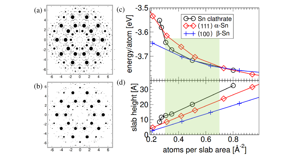
Fig. 7(a,b) shows that diffraction patterns of decagonal Sn-clathrate and the bulk -Al-Pd-Mn phases parallel to their common 5-fold axis exhibit striking similarity in both positions and intensity of the strong diffraction peaks. The apparent symmetry of the diffraction pattern is 10-fold in both cases, due to the presence of inversion symmetry in -Al-Pd-Mn, and 10-fold screw axis in -clathrate. The similarity of the patterns supports the Sn clathrate structural hypothesis.
III.7 Energetics of unsupported Sn slabs
We further test the clathrate structural hypothesis by comparing the cohesive energies of the unsupported Sn slabs. We constructed reference series of the slabs of -Sn with the surface normal to (111) direction, and of -Sn with the surface normal to (100). These surfaces are flat planes in both cases, in -Sn atoms on the surface are 3-fold coordinated, in -Sn it is 5-fold coordinated (when we cut off the first coordination shell at about 3.3Å).
For clathrates, we require that all the surface atoms have coordination equal to 3, like -Sn. This can be realized by growing the clathrate layer in discrete steps, by completing all (open) cages whose centers are nearest to the current surface. This strategy allows us to circumvent the difficulty of growing the “sparse” clathrate structure that does not contain well defined flat layers, but rather coalesces sharing pentagonal/hexagonal faces between the neighboring cages.
In decagonal clathrates, the cage centers are located on four heights per 12.7Å vertical repeat: dodecahedra decorate the R-T tiling vertices at fractional height coordinates = 0 and 0.5. The mid-edge and tile-interiors cage centers are all located at = 0.25 and = 0.75. From this we derived the aforementioned strategy for the slab construction: the surfaces are formed by completing all cages with next higher fractional coordinate .
To represent the slab of the decagonal clathrate, we chose periodic approximant from Fig. 6(c). Slabs for all three structures, , and decagonal clathrate approximant were fully optimized by relaxing ionic positions and lattice parameters until the average DFT force was less than 0.05 eV/Å, followed by single final self-consistent iteration with fixed geometry.
Energetics of sufficiently thick layers are characterized by bulk and surface energies, , where is bulk energy per Sn atom, is energy of the layer consisting of N atoms per periodic box, and is the surface area. The bulk energy of the clathrate Sn approximant is stable compared to that of -Sn by 11 meV/atom. In contrast, the former is unstable against -Sn by 35 meV/atom. The surface energies, on the other hand show opposite trend, reaching minimum for -Sn slabs, with 0.025 meV/, followed closely by clathrate (0.27 meV/Å2), and -Sn (0.41 meV/Å2). This result is consistent with and surface energies calculated in Ref. Hormann15, , leading to prediction that sufficiently small Sn nano-particles will consist of -Sn even in the low-temperature limit (although that work does not include the possibility of nanoparticles based on clathrate cages).
In order to capture energetic competition between the three families of slabs, we evaluate and plot DFT energies of the slabs as a function of the number of atoms per unit area normal to the slab surfaces. The results are shown in Fig. 7(c), which plots cohesive energy/atom as a function of the area coverage. Fig. 7(d) shows the height defined as a difference of the topmost and bottom atom coordinates (- ).
For thinnest slabs with coverages up to about 0.4 atom/Å2, the most stable structure is -Sn. The clathrate approximant performs excellently for layer thickness exceeding approximately its one periodic repeat (about 12.7Å), or twice the 5-fold diameter of the fundamental dodecahedral cage: in the 0.3-0.7 atom/Å2 covering range, for slab heights between 10-35Å, it is more stable than -Sn [the range is shaded in light green in Fig. 7(c,d)]. It approximately equals energy of -Sn in the range 0.5-0.7 atom/Å2 or 2-3 nm slab thickness. Finally, when the coverage exceeds 0.7 atoms/Å2 or slab thickness 3 nm approaching the bulk limit, the most stable structure is -Sn.
III.8 Photoemission spectroscopy and density of states from the clathrate model
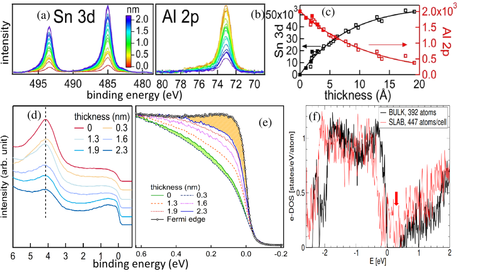
In Fig. 8(a,b), Sn 3 and Al 2 XPS core level spectra that appear at 485 eV and 73.1 eV, respectively, show no change in their binding energies with Sn coverage. This is a significant observation because core-level binding energies are sensitive to the transfer of electronic charge from the adsorbate to the substrate, which obviously can be ruled out in this case. Absence of core level shift or change in the shape also excludes the possibility of any alloying or intermixing of Sn with the substrate. This observation also implies a propensity for condensed island growthShukla_prb06 as also shown in Fig. 2(a), indicating the dominance of adsorbate-adsorbate interaction. The Sn 3 core level binding energy (485 eV) is similar to that of -SnHegde , indicating the similarity of the quasiperiodic Sn layer with that of -Sn, thus reaffirming the clathrate model where hybridization dominates. In Fig. 8(c), the intensity variation of the Sn 3 and Al 2 XPS core-level spectra exhibits exponential trend as a function of thickness indicating a layered growth, as also shown by STM. Fig. 8(d) depicts the valence band of Sn/-Al-Pd-Mn, where the prominent peak at 4 eV binding energy arises from Pd 4-like states. It decreases in intensity with Sn deposition, but its binding energy remains unchanged lending further support to the conclusions drawn from the core-level spectra [Fig. 8(a,b)].
The stability of quasicrystals has been related to the existence of a pseudogap in the electronic DOS around the Fermi level () originating from the interaction between the Fermi surface and the quasi-Brillouin zone of the quasicrystalNayak_prl12 ; Hafner92 ; Stadnik_prl96 . In the valence band spectrum of -Al-Pd-Mn [Fig. 8(d)], the pseudogap was ascribed to the rounded shape of the spectral function close to Stadnik_prl96 . With Sn deposition up to 1 ML (0.3 nm), we observe an interesting change in its shape [Fig. 8(e)]: the spectral weight decreases compared to -Al-Pd-Mn, indicating a deepening of the pseudogap for the Sn monolayer, as is evident from the green shaded region. The pseudogap is observed up to the thickness of 2.3 nm (orange shaded region), as shown by the comparison with a metal Fermi edge in electrical contact with the specimen. However, for thicker layers, the pseudogap becomes shallower compared to the substrate, which is possibly related to the increase in disorder, as also shown by the relative weakening of the LEED spots, as discussed earlier in Section III.C.
The DOS for relaxed bulk and slab Sn clathrate is shown in Fig. 8(f). It is interesting to note that the bulk Sn quasiperiodic clathrate is semiconducting with a band gap of about 0.4 eV, in contrast to bulk -Al-Pd-Mn that shows a pseudogapKH . In contrast to bulk, the DOS for the slab of Sn quasiperiodic clathrate shows a pronounced pseudogap with the minimum at 0.3 eV (red arrow), the states near having almost equal contributions from the Sn and Sn states, while the contribution from the states is marginal. The pseudogap is deeper compared to -Al-Pd-Mn, where the DOS was calculated for MS and M slabsKH . Thus, the Sn clathrate model explains the interesting observation from photoemission that the pseudogap is deeper for the Sn monolayer compared to the substrate -Al-Pd-Mn. It is worth to note that the inter atomic bonding in Sn is different from Pb, where a wider pseudogap was reported from scanning tunneling spectroscopy, but it was later ascribed to the splitting of Pb 6 band due to large spin-orbit couplingLedieu_prb08 ; Krajci_PbAPM_prb10 ; Sharma13 . Pb does not have hybridization since the and bands are clearly separated, and thus the bonding is mediated by orbitals only. Here, the deepening of the pseudogap around results from formation of the puckered clathrate structure with high covalency and bonding between the Sn atoms. The clathrate structures perfectly support the bonding scheme, with exclusively tetrahedral local environments like in -Sn structure - but while in the latter the empty spaces are condensed into flat interlayer area, in clathrates they are isolated in four types of approximately spherical cages (Fig. 5).
III.9 The relaxed clathrate model and the STM motifs
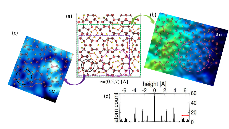
The structure of the most optimal surface of the Sn clathrate obtained by relaxing the atom positions in our DFT calculation is shown in Fig. 9(a). We find that it exhibits protruding dodecagons projecting down on the tiling vertex positions, while the pentagonal caps of the dodecahedral cages suffer considerable distortion. The height distribution of the Sn atoms shows existence of different layers in the slab [Fig. 9(d)]. However, their widths are considerable and in particular, the surface region shows that the spread in is 2Å (red double arrow). This demonstrates that the surface is corrugated, in agreement with STM that shows large root mean square roughness (Section III.C). Such large corrugation arises because the clathrate structure fills the space very loosely and is made of large empty cages, and there may be wells even 4Å deep. Moreover, in reality, all the atom positions of the layer are not occupied and disorder is present, in agreement with the results from LEED discussed in Section III.C.
The relaxed clathrate structure is in good agreement with STM and the motifs are also reproduced. For example, in Fig. 9(b), a part of the clathrate structure enclosed by green dashed rectangle is overlaid on a STM image from 3 nm thick Sn layer that includes a crown motif (encircled by pink dashed circle) after inflation and the agreement is found to be satisfying. -inflation is well known in quasicrystals due to their self-similar nature, for example, in -Al-Pd-Mn, the fundamental intercluster linkage of 7.75Å is inflated along the 2- fold direction, while 3 inflation is observed along 5-fold or 3-fold directions. 3 inflation has also been reported in a binary quasicrystal Yb-Cd with the formation of cluster of clustersTakakura07 . Fig. 9(c) provides another example, where a STM image containing a hexagonal tile centered motif (encircled by black dashed circle) observed for 1 ML Sn is reproduced by a hexagon and the pentagons surrounding it from the violet dashed rectangle in Fig. 9(a) with inflation. Thus, the relaxed clathrate model is able to reproduce the STM images [Fig. 9(b, c)], which reconfirms the validity of this structural model.
III.10 Nucleation and compatibility of the Sn clathrate structure with -Al-Pd-Mn
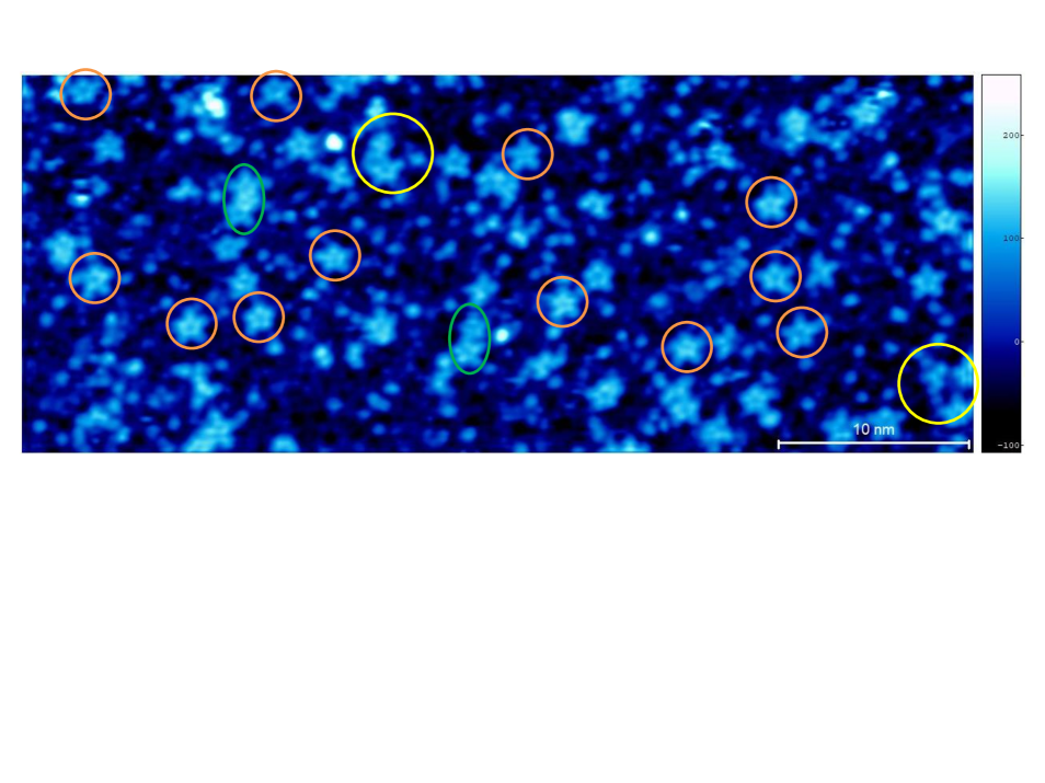
In this section, in order to find the genesis of the Sn clathrate structure and establish its compatibility with the substrate -Al-Pd-Mn, we have studied the sub-monolayer coverages of Sn by STM to identify the nucleation centers. We find occurrence of pentagonal clusters that look like flowers with five bright petals at 0.2 ML coverage (encircled by orange dashes in [Fig. 10(a)], a larger area image is shown in Fig. S8supplement ). These clusters are formed on specific areas of the 5-fold surface recognized in STM images as white flowersKHLM , and so we call them as the Sn white flower (SnWF) clusters. As shown in Fig. S8 by orange circles, the SnWF’s are oriented in the same direction and are mostly isolated. However, we are able to identify regions, for example, inside the red rectangle in Fig. 10(a) that has two SnWF’s that are nearest neighbors.
Similar five-fold clusters have also been observed for PbLedieuPbAPMprb09 and BiSmerdon_prb08 , which on the -Al-Pd-Mn surface exhibit pseudomorphic growth up to a monolayer. In both systems, these five-fold clusters have been dubbed as the starfish clusters. On the -Al-Pd-Mn surface, deposited Sn forms thick layer with the structure of quasicrystalline clathrate. The SnWF clusters appearing at the sub-monolayer coverage play here an important role of nucleation centers for growth of the quasicrystalline layer.
To explain the role of the SnWF clusters we use the model of the 5/3 approximant of -Al-Pd-MnKH ; KWHKM . The structure of the 5-fold surface that can be described by the Penrose P1 tiling with an edge length of 7.76ÅKH [black lines in Fig. 10(c)]. The tiling consists of pentagon, thin rhombus, star, and boat. The bulk structure of -Al-Pd-Mn can be interpreted in terms of the pseudo-Mackay (pMC) clusters. On the 5-fold surface, the pentagonal tiles represent sections over these pMC clusters. The equatorial section of the pMC cluster has a Mn atom in the center of the pentagonal tile [Fig. 10(c)] and in the STM image this motif is seen as the white flower mentioned aboveKHLM . If the center of the pMC is deeper below the surface plane, this part of the surface corresponds to another characteristic pattern known as the dark starKHLM . In the STM image of the bare surface shown in Fig. S1(c)supplement , motifs of the white flower and the dark star can be well recognized.
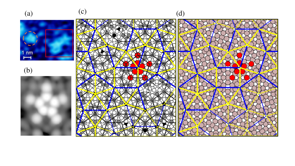
At the submonolayer coverage, the SnWF cluster formed on the white flowers consists of 10 adatomsKrajci_PbAPM_prb10 , as shown by the red atoms in Fig. 10(c). The calculated STM image of the SnWF is shown in Fig. 10(b), where shape is similar to that observed in the experiment [Fig. 10(a) and Fig. S8]. The central pentagon around this would show up as bright maxima in the STM images. To examine the compatibility of the SnWF with the clathrate structure, it is interesting to compare the configuration of 10 Sn adatoms forming the SnWF cluster [Fig. 10(c)](marked red) with the structure of the clathrate layer [Fig. 10(d)]. The clathrate structure consists of regular dodecahedral cages of Sn atoms. The dodecahedra are centered at the vertices of the R-T tiling [Fig. 10(d)]. The top (or bottom) pentagonal face of the dodecahedron corresponds to the inner pentagon of the SnWF cluster.
The edges of the R-T tiling have two different lengths, the shorter (yellow) and longer (blue). In the -Al-Pd-Mn structure, the length = 12.55Å corresponds to the distance between two pMC clusters along the two-fold directions. In the clathrate layer, each of the two neighboring dodecahedral cages at the distance of the longer edge are connected over one Sn atom. This atom corresponds to the Sn atom from the outer pentagonal ring of the SnWF cluster. The bonding topology of the SnWF cluster is thus closely related to the structure of the Sn-clathrate and is a valid part of the clathrate structure. The SnWF’s can thus serve as nucleation centers for growth of the quasiperiodic Sn adlayer with the clathrate structure.
On the other side, as the bulk structure of clathrate is different from the bulk structure of -Al-Pd-Mn, there are also significant differences between the SnWF configurations on the -Al-Pd-Mn surface and in the clathrate adlayer. On the 5-fold Al-Pd-Mn surface, the SnWF cluster has essentially a planar structure and the interatomic bonding has a metallic character. All the SnWF clusters on the surface have only one pentagonal orientation. In the atomic structure of the clathrate, the inner and outer pentagons of the SnWF clusters are at different heights. The interatomic bonding has the covalent sp3 character. They have both pentagonal orientations. The compatibility of the interface between the -Al-Pd-Mn surface and the clathrate adlayer helps to stabilize the clathrate structure and prevents its conversion to a more stable crystalline structure.
Comparing Fig. 10(c) and (d), one can see that the arrangement of the tiles in a large part of the tilings on both models marked by thick blue and yellow lines are exactly the same. The parts of the R-T tilings on the -Al-Pd-Mn and Sn clathrate surfaces with different arrangement of the tiles are marked by thinner lines. The reason why both tilings are not the same on the whole surface areas of the 5/3 approximants is the following: out of 4 tiles of the P1 tiling describing ordering of atoms on the -Al-Pd-Mn surface, three of them - pentagon, thin rhombus and star are compatible with the R-T tiling, but the boat tile contradicts the R-T ordering. On the 5/3 approximant model of the -Al-Pd-Mn surface, there are 2 boat tiles [dashed black lines in Fig. 10(c)]. Around the boat tiles, the ordering of -Al-Pd-Mn atoms can be again described by the R-T tiling (thin blue and yellow lines), however, with somewhat different arrangement of the tiles than in the clathrate model [Fig. 10(d)]. The boat tiles can thus induce defects in the R-T tiling. The presence of the boat tiles can be the origin of the observed partial disorder in the Sn adlayer.
IV CONCLUSIONS
Our work demonstrates formation of a new quasicrystalline structure in a thick Sn layer up to a thickness of atleast 4 nm. Based on multiple evidences from both experiment and theory, we propose a quasiperiodic clathrate structural model for the Sn layer. Sn retains quasicrystallinity up to a thickness that is highest reported so far for any element, and this is almost in the realm of bulk-like growth, where the influence of the substrate potential is negligible. The STM motifs (crown, wheel and hexagonal tile centered motif in Fig. 1) and the LEED IV curves (Fig. S3 of SMsupplement ) of the Sn monolayer are different from -Al-Pd-Mn that is described by the Penrose P1 tiling. The motifs of the thick Sn layer are similar to the motifs of the first layer. This shows a structural difference between the Sn layer and the substrate, indicating that Sn grows with its intrinsic quasiperiodic structure and the substrate is unable to force a pseudomorphic growth. The role of the substrate is solely to suppress initial formation of any stable crystalline forms of Sn. Photoemission spectroscopy shows that the pseudogap around the Fermi level is deeper for the first Sn monolayer compared to -Al-Pd-Mn and exists for the thick layer, indicating its stability. Using density functional theory, a comparative study of the free slab energies shows that surface energy favors clathrate over -tin up to about 4 nm layer thickness, and matches -tin for narrow window of slab thickness of 2-3 nm. The bulk clathrate exhibits gap opening near Fermi energy, while the free slab form exhibits a pronouced pseudogap that explains the photoemission result. The STM images and the motifs observed on the Sn layer show good agreement with the proposed clathrate model. The SnWF clusters constitute the nucleation centers for growth of the quasiperiodic Sn adlayer since these are a valid part of the Sn clathrate structure. It is realized on the -Al-Pd-Mn surface because the cluster-cluster separations (12.55 Å) observed on the latter enjoy magic consistency with the cage-cage separations in the Sn clathrate. Last but not the least, although here we do not observe Sn quasicrystal in the bulk form, the lower bulk total energy of the quasiperiodic Sn clathrate compared to -Sn suggests that bulk quasicrystalline Sn might also exist in some part of its phase diagram.
V ACKNOWLEDGMENTS
M. M. and M.K. thank support from the Slovak Grant Agency VEGA (No. 2/0082/17), and from APVV (No. 15-0621). Part of the calculations were performed in the Computing Center of the Slovak Academy of Sciences using the supercomputing infrastructure acquired under projects ITMS 26230120002 and 26210120002. K.P. thanks CSC–IT Center for Science and the Academy of Finland under Grant No. 277829. Karsten Horn is thanked for his constructive suggestions and support. M. Maniraj is grateful to the C.S.I.R, New Delhi for research fellowship. J. Nayak, P. Bhakuni and M. Balal are thanked for assistance during some of the experiments.
Work by TAL and DLS was supported by the U.S. Department of Energy (DOE), Office of Science, Basic Energy Sciences, Materials Science and Engineering Division. The -Al-Pd-Mn substrate was synthesized at the Materials Preparation Center, at the Ames Laboratory, which is operated for the U.S. DOE by Iowa State University under contract DE-AC02-07CH11358.
Electronic address of the corresponding authors:
∗Marek.Mihalkovic@savba.sk,
∗∗Marian.Krajci@savba.sk,
‡barmansr@gmail.com
References
- (1) D. Shechtman, I. Blech, D. Gratias, J. W. Cahn, Metallic Phase with Long-Range Orientational Order and No Translational Symmetry, Phys. Rev. Lett. 53, 1951-1953 (1984).
- (2) R. Penrose, The role of aesthetics in pure and applied mathematical research, Bull. Inst. Maths & its Applns. 10, 266-271 (1974).
- (3) L. Bindi, P. J. Steinhardt, N. Yao, P. J. Lu, Natural quasicrystals, Science 324, 1306-1308 (2009).
- (4) A. P. Tsai, J. Q. Guo, E. Abe, H. Takakura, T. J. Sato, A stable binary quasicrystal, Nature 408, 537-538 (2000).
- (5) D. V. Talapin, V. E. Shevchenko, I. M. Bodnarchuk, X. Ye, J. Chen, C. B. Murray, Quasicrystalline order in self-assembled binary nanoparticle superlattices, Nature 461, 964967 (2009).
- (6) S. Fischer, A. Exner, K. Zielske, J. Perlich, S. Deloudi, W. Steurer, P. Lindner, S. Frster, Colloidal quasicrystals with 12-fold and 18-fold diffraction symmetry, Proc. Natl. Acad. Sci. USA 108, 1810-1814 (2011).
- (7) S. Frster, K. Meinel, R. Hammer, M. Trautmann, W. Widdra, Quasicrystalline structure formation in a classical crystalline thin-film system, Nature 502, 215-218 (2013).
- (8) C. Xiao, N. Fujita, K. Miyasaka, Y. Sakamoto, O. Terasaki, Dodecagonal tiling in mesoporous silica, Nature 487, 349-353 (2012).
- (9) X. Ye, J. Chen, M. E. Irrgang, M. Engel, A. Dong, S. C. Glotzer, C. B. Murray, Quasicrystalline nanocrystal superlattice with partial matching rules, Nat. Mater. 16, 214-220 (2017).
- (10) Y. E. Kraus, O. Zilberberg, Quasiperiodicity and topology transcend dimensions, Nature. Phys. 12, 624-626 (2016).
- (11) D. Zhou, L. Zhang, X. Mao, Topological Boundary Floppy Modes in Quasicrystals, Phys. Rev. X 9, 021054 (2019).
- (12) J. Y. Park, D. F. Ogletree, M. Salmeron, R. A. Ribeiro, P. C. Canfield, C. J. Jenks, P. A. Thiel, High Frictional Anisotropy of Periodic and Aperiodic Directions on a Quasicrystal Surface, Science 309, 1354-1356 (2005).
- (13) J. M. Dubois, Properties- and applications of quasicrystals and complex metallic alloys. Chem. Soc. Rev. 41, 6760 (2012).
- (14) K. J. Franke, H. R. Sharma, W. Theis, P. Gille, Ph. Ebert, and K. H. Rieder, Quasicrystalline Epitaxial Single Element Monolayers on Icosahedral Al-Pd-Mn and Decagonal Al-Ni-Co Quasicrystal Surfaces, Phys. Rev. Lett. 89, 156104 (2002).
- (15) M. Shimoda, J. Q. Guo, T. J. Sato, A. -P. Tsai, Thin Sn film induced by surface diffusion on a quasiperiodic surface of decagonal Al-Ni-Co , J. Non-Cryst. Solids 334, 505-508 (2004).
- (16) H. R. Sharma, M. Shimoda, A. R. Ross, T. A. Lograsso, A. -P. Tsai, Real-space observation of quasicrystalline Sn monolayer formed on the fivefold surface of icosahedral Al-Cu-Fe quasicrystal, Phys. Rev. B 72, 045428 (2005).
- (17) M. Krajčí, J. Hafner, Ab initio study of quasiperiodic monolayers on a fivefold -Al-Pd-Mn surface, Phys. Rev. B 71, 184207 (2005).
- (18) A. K. Shukla, R. S. Dhaka, C. Biswas, S. Banik, S. R. Barman, K. Horn, Ph. Ebert, K. Urban, Growth and electronic structure of alkali-metal adlayers on icosahedral Al70.5Pd21Mn8.5, Phys. Rev. B 73, 054432 (2006).
- (19) J. Ledieu, L. Leung, L. H. Wearing, R. McGrath, T. A. Lograsso, D. Wu, V. Fournée, Self-assembly, structure, and electronic properties of a quasiperiodic lead monolayer, Phys. Rev. B 77, 073409 (2008).
- (20) J. A. Smerdon, J. K. Parle, L. H. Wearing, T. A. Lograsso, A. R. Ross, R. McGrath, Nucleation and growth of a quasicrystalline monolayer: Bi adsorption on the fivefold surface of , Phys. Rev. B 78, 075407 (2008).
- (21) J. Ledieu, M. Krajčí, J. Hafner, L. Leung, L. H. Wearing, R. McGrath, T. A. Lograsso and D. Wus, V. Fournée, Nucleation of Pb starfish clusters on the five-fold Al-Pd-Mn quasicrystal surface, Phys. Rev. B 79, 165430 (2009).
- (22) H. R. Sharma, V. Fournée, M. Shimoda, A. R. Ross, T. A. Lograsso, P. Gille, and A. P. Tsai, Growth of Bi thin films on quasicrystal surfaces, Phys. Rev. B 78, 155416 (2008).
- (23) A. K. Shukla R. S. Dhaka, S. W. D’Souza, S. Singh, D. Wu, T. A. Lograsso, M. Krajčí, J. Hafner, K. Horn, S. R. Barman, Quasiperiodic layers of free-electron metals studied using electron diffraction, Phys. Rev. B 79, 134206 (2009).
- (24) M. Krajčí, J. Hafner, J. Ledieu, V. Fournée, R. McGrath, Quasiperiodic Pb monolayer on the fivefold i-Al-Pd-Mn surface: Structure and electronic properties, Phys. Rev. B 82, 085417 (2010).
- (25) H. R. Sharma, K. Nozawa, J. A. Smerdon, P. J. Nugent, I. McLeod, V. R. Dhanak, M. Shimoda, Y. Ishii, A. P. Tsai, R. McGrath, Templated three-dimensional growth of quasicrystalline lead, Nature Commun. 4, 2715 (2013).
- (26) S. S. Hars, J. Hafner, J. Ledieu, V. Fournée, R. McGrath, Growth of a bismuth thin film on the five-fold surface of the icosahedral Ag-In-Yb quasicrystal, Surf. Sci. 678, 222-227 (2018).
- (27) J. Ledieu, J. T. Hoeft, D. E. Reid, J. A. Smerdon, R. D. Diehl, T. A. Lograsso, A. R. Ross, R. McGrath, Pseudomorphic Growth of a Single Element Quasiperiodic Ultrathin Film on a Quasicrystal Substrate, Phys. Rev. Lett. 92, 135507 (2004).
- (28) A. R. Smith, K.-J. Chao, Q. Niu, C.-K. Shih, Formation of atomically flat silver films on GaAs with a silver mean quasi-periodicity, Science 273, 226-228 (1996).
- (29) M. Engel, P. F. Damasceno, C. L. Phillips, S. C. Glotzer, Computational self-assembly of a one-component icosahedral quasicrystal, Nature Mat. 14, 109-116 (2015).
- (30) A. K. Shukla, S. Banik, R. S. Dhaka, C. Biswas, S. R. Barman, H. Haak, Versatile UHV compatible Knudsen type effusion cell, Rev. Sci. Instrum. 75, 4467-4470 (2004).
- (31) H. Shinotsuka, S. Tanuma, C. J. Powell, D. R. Penn, Calculations of electron inelastic mean free paths. X. Data for 41 elemental solids over the 50eV to 200keV range with the relativistic full Penn algorithm, Surf. Intf. Anal. 47, 871 (2015).
- (32) G. Kress, J. Furthmuller, Efficiency of ab-initio total energy calculations for metals and semiconductors using a plane-wave basis set, Comp. Mater. Sci. 6, 15-50 (1996).
- (33) G. Kresse and D. Joubert, From ultrasoft pseudopotentials to the projector augmented-wave method, Phys. Rev. B 59, 1758-1775 (1999).
- (34) J. P. Perdew, J. A. Chevary, S. H. Vosko, K. A. Jackson, M. R. Pederson, D. J. Singh, C. Fiolhais, Atoms, molecules, solids, and surfaces: Applications of the generalized gradient approximation for exchange and correlation, Phys. Rev. B 46, 6671-6687 (1992).
- (35) See Supplemental Material at [ ] for Figs. S1-S8 and four video files showing LEED patterns as a function of beam energy.
- (36) M. Gierer, M. A. Van Hove, A. I. Goldman, Z. Shen, S.-L. Chang, C. J. Jenks, C.-M. Zhang, P. A. Thiel, Structural Analysis of the Fivefold Symmetric Surface of the Al70Pd21Mn9 Quasicrystal by Low Energy Electron Diffraction, Phys. Rev. Lett. 78, 467470 (1997).
- (37) L. Barbier, D. Le Floc’h, Y. Calvayrac, D. Gratias, Identification of the Atomic Structure of the Fivefold Surface of an Icosahedral Al-Pd-Mn Quasicrystal: Helium Diffraction and Scanning Tunneling Microscopy Studies, Phys. Rev. Lett. 88, 085506 (2002).
- (38) V. E. Bauer, Phenomenological theory of crystal deposition on surfaces, Z. Kristallogr. Krist. 110, 372-394 (1958).
- (39) W. R. Tyson, W. A. Miller, Surface free energies of solid metals estimation from liquid surface tension measurements, Surf. Sci. 62, 267-276 (1977).
- (40) L. Vitos, A. V. Ruban, H. L. Skriver, J. Kollar, The surface energy of metals, Surf. Sci. 411, 186-202 (1998).
- (41) J. M. Dubois, M.-C. de Weerd, J. Brenner, M. Sales, G. Mozdzen, A. Merstallinger, E. Belin-Ferré, Surface energy of complex - and simple - metallic compounds as derived from friction test in vacuum, Phil. Mag. 86, 797-805 (2006).
- (42) H. R. Sharma, M. Shimoda, A. P. Tsai, Quasicrystal surfaces: structure and growth of atomic layers, Adv. Phys. 56, 403-464 (2007).
- (43) B. Bolliger, V. E. Dmitrienko, M. Erbudak, R. Lscher, H.-U. Missen, A. R. Kortan, Epitactic textures of fcc Al on icosahedral Al-Pd-Mn quasicrystal, Phy. Rev. B 63, 052203 (2001).
- (44) N. D. Lang, W. Kohn, Theory of metal surfaces: Charge density and surface energy, Phys. Rev. B 1, 4555-4568 (1970).
- (45) A. M. Guloy, R. Ramlau, Z. Tang, W. Schnelle, M. Baitinger, Y. Grin, A guest-free germanium clathrate, Nature 443, 320-323 (2006).
- (46) J. Gryko, P. F. McMillan, R. F. Marzke, G. K. Ramachandran, D. Patton, S. K. Deb, O. F. Sankey, Low-density framework form of crystalline silicon with a wide optical band gap, Phy. Rev.B 62, R7707-R7710 (2000).
- (47) E. Cockayne, Dense quasiperiodic decagonal disc packing, Phys. Rev. B 51, 14958 (1995).
- (48) F. C. Frank, J. S. Kasper, Complex Alloy Structures Regarded as Sphere Packings. I. Definitions and Basic Principles, Acta. Crystallogr. 11, 184 (1958).
- (49) M. O’Keeffe, G. B. Adams, O. F. Sankey, Duals of Frank-Kasper structures as C, Si and Ge clathrates: energetics and structure, Phil. Mag. Lett. 78, 21 (1998).
- (50) F. C. Frank, J. S. Kasper, Complex Alloy Structures Regarded as Sphere Packings. II. Analysis and classification of Representative Structures, Acta. Crystallogr. 12, 483 (1959).
- (51) S. Iwami, T. Ishimasa, Dodecagonal quasicrystal in Mn-based quaternary alloys containing Cr, Ni and Si, Phil. Mag. Lett. 95, 229 (2015).
- (52) X. Zeng , G. Ungar, Inflation rules of square-triangle tilings: from approximants to dodecagonal liquid quasicrystals, Phil. Mag. 86, 1093-1103 (2006).
- (53) G. Bergman, J. L. T. Waugh, L. Pauling, Crystal Structure of the Intermetallic Compound Mg32(AI,Zn)49 and Related Phases, Nature 169, 1057-1058 (1952).
- (54) C. L. Henley, V. Elser, Quasicrystal structure of (Al, Zn)49Mg, Phil. Mag. Lett. 53, L59-L66 (1986).
- (55) N. G. Hrmann, A. Gross, P. Kaghazchi, Semiconductor- Metal transition induced by nano scale stabilization, Phys. Chem. Chem. Phys. 17, 5569-5573 (2015).
- (56) R. I. Hegde, Core level binding energy shifts in dilute tin alloys, Surf. Intf. Anal. 4, 204 (1982).
- (57) J. Nayak, M. Maniraj, A. Rai, S. Singh, P. Rajput, A. Gloskovskii, J. Zegenhagen, D. L. Schlagel, T. A. Lograsso, K. Horn, and S. R. Barman, Bulk Electronic Structure of Quasicrystals, Phys. Rev. Lett. 109, 216403 (2012).
- (58) J. Hafner, M. Krajčí, Electronic structure and stability of quasicrystals: Quasiperiodic dispersion relations and pseudogaps, Phys. Rev. Lett. 68, 2321-2324 (1992).
- (59) Z. M. Stadnik, D. Purdie, M. Garnier, Y. Baer, A.-P. Tsai, A. Inoue, K. Edagawa, S. Takeuchi, Electronic Structure of Icosahedral Alloys Studied by Ultrahigh Energy Resolution Photoemission Spectroscopy, Phys. Rev. Lett. 77, 1777-1780 (1996).
- (60) M. Krajčí, J. Hafner, Structure, stability, and electronic properties of the i-AlPdMn quasicrystalline surface, Phys. Rev. B 71, 054202 (2005).
- (61) H. Takakura, C. P. Gomez, A. Yamamoto, M. D. Boissieu, A. P. Tsai, Atomic structure of the binary icosahedral Yb–Cd quasicrystal, Nature Mater. 6, 58-63 (2007).
- (62) M. Krajčí, M. Windisch, J. Hafner G. Kresse, M. Mihalkovic, Atomic and electronic structure of icosahedral Al-Pd-Mn alloys and approximant phases, Phys. Rev. B 51, 17355 (1995).
- (63) M. Krajčí, J. Hafner J. Ledieu, R. McMgrath, Surface vacancies at the fivefold icosahedral Al-Pd-Mn quasicrystal surface: A comparison of ab initio calculated and experimental STM images, Phys. Rev. B 73, 024202 (2006).
Supplementary material to the manuscript entitled:
Quasiperiodic ordering in thick Sn layer on -Al-Pd-Mn: A possible quasicrystalline clathrate
The supplementary material contains eight figures (S1S8) and of four video files named “3nmleed” for 3 nm, “1.8nmleed” for 1.8 nm, “1nmleed” for 1 nm and “0.25nmleed” for the 0.25 nm or 1 ML Sn layer thicknesses. The video files show a sequence of LEED patterns as a function of beam energy, as indicated in the top left corner for each pattern. The video files are uploaded separately.
