Suppression of the superconductivity in ultrathin amorphous Mo78Ge22 thin films observed by STM
Abstract
In contact with a superconductor a normal metal modifies its properties due to Andreev reflection. In the current work the local density of states (LDOS) of superconductor - normal metal Mo78Ge22 - Au bilayers are studied by means of STM applied from the Au side. Three bilayers have been prepared on silicate glass substrate consisting of 100, 10 and 5 nm MoGe thin films covered always by 5 nm Au layer. The tunneling spectra were measured at temperatures from 0.5 K to 7 K. The two-dimensional cross-correlation between topography and normalized zero-bias conductance (ZBC) indicates a proximity effect between 100 and 10 nm MoGe thin films and Au layer where a superconducting gap slightly smaller than that of bulk MoGe is observed. The effect of the thinnest 5 nm MoGe layer on Au leads to much smaller gap moreover the LDOS reveals almost completely suppressed coherence peaks. This is attributed to a strong pair-breaking effect of spin-flip processes at the interface between MoGe films and the substrate.
I Introduction
Disorder and reduced dimensionality affect the physical properties of metallic systems in several ways Anderson et al. (1979); Altshuler et al. (1980). Strong diffusion leads to localization of electrons and a related enhancement of the Coulomb interaction. In a system of lower dimensions, the coupling to disorder increases and pronounced effects are expected.
Amorphous MoGe thin films are suitable system for studying the interplay between superconductivity and reduced dimensionality. Several transport experiments showed a reduction of the superconducting transition temperature Graybeal and Beasley (1984); Strongin et al. (1970) which could lead to superconductor - insulator transition Haviland et al. (1989); Szabó et al. (2016).
In a contact with a normal metal the superconductor wave function is changed by the proximity effect De Gennes (1964). On the normal-metal side a minigap or suppressed superconducting gap is induced Belzig et al. (1996).
In this work, the local density of states (LDOS) has been measured by means of the scanning-tunneling-microscope (STM) technique. The two-dimensional cross correlation between the topography of locally varying Au thickness and the tunneling zero-bias conductance (ZBC) for 10 nm and 100 nm MoGe bilayer samples indicate a presence of the proximity effect in the LDOS of Au overlayer. The LDOS spectra on Au reveal the gap which is only slightly suppressed in comparison with that in bulk MoGe. It means that down to 10 nm thickness the superconducting properties of MoGe are not changing. In the bilayer with 5 nm MoGe the tunneling spectrum shows a high ZBC and strongly suppressed coherence peaks. Such a strong suppression of superconducting LDOS in the same 5 nm Au layer cannot come just from proximity effect. Also there is no correlation between the topography and ZBC. Then, the proximity effect is not sufficient to explain the spectra measured on Au but superconductivity in the 5 nm MoGe is strongly suppressed. We consider a strong pair breaking due to the spin-flip processes at the interface between MoGe and the glass substrate. Consequently, superconductivity in MoGe will be supressed as well by an inverse proximity effect.
II Experimental details
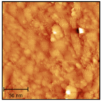
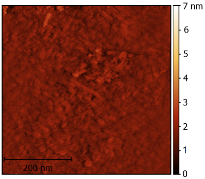
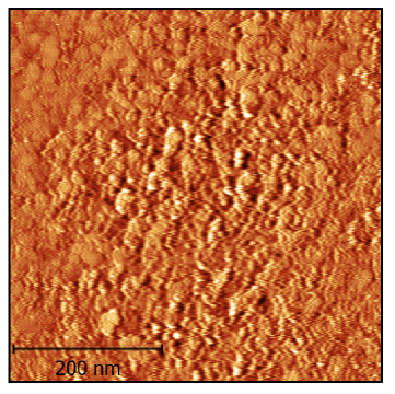
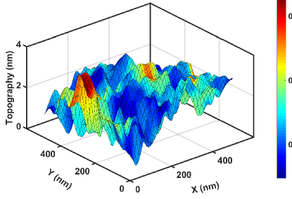
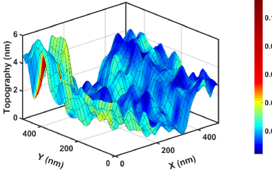
A magnetron sputtering technique was used to produce MoGe thin films with thicknesses of 5, 10, and 100 nm covered by Au layer with thickness of 5 nm. The films were deposited on commercially available silicate glass slides of 10 mm x 10 mm x 0.5 mm size. MoGe was sputtered on the rotating sample holder from a commercial single composite target with a 99.9+ % purity. The sputtering conditions for MoGe were: chamber pressure 3.710-10 Pa, argon pressure 2.210-5 Pa, DC target power 100 W, substrate temperature 22 ∘C, the sputtering rate is 0.59 Ås-1. Immediately after MoGe deposition, the Au thin film was sputtered with the rate 4.54 Ås-1 to prevent the oxidation. The thickness of the sputtered films was controlled by quartz crystal microbalance device. The topography of the samples is shown in Fig. 1. RMS roughnesses of 5 nm, 10 nm and 100 nm MoGe thin films are 1.09 nm, 0.38 nm and 0.76 nm, respectively. The sizes of topography are 500 nm x 500 nm for 10 and 100 nm thin films and 250 nm x 250 nm for 5 nm film.
The scanning tunneling microscopy and spectroscopy experiments were performed by means of a homemade STM head Samuely et al. (2013) controlled by the Nanotec s Dulcinea SPM
electronics. The head is inserted in a commercial Janis SSV cryomagnetic system with 3He refrigerator and the Au tip was prepared in-situ by repetitive impaling into the bulk Au sample and subsequent slow retraction.
The procedure was repeated until the current position dependence exhibited the conductance quantization and single-atom contact phenomena inherent for gold Agrait et al. (2003). The sample was grounded while bias voltage was applied to the tip with the tunneling resistance 10 M.
The individual spectra have been measured in temperature range between 0.5 K and 7 K. At the lowest temperature we have also performed the current imaging tunneling spectroscopy (CITS) providing the spectral maps at each point of the topography.
III Results and discussion
The experimental conductance spectra were analyzed assuming normal metal - insulator - superconductor (NIS) contact described by eq. Tinkham (2008):
| (1) |
where is a charge of electron, is a tunneling current, is a bias voltage between Au tip and the sample, is experimental differential conductance, – normal-state differential conductance, is superconducting density of states (SDOS), is the normal-state density of states at Fermi level, and is the Fermi-Dirac distribution function. The superconducting density of states was taken in the Dynes form Dynes et al. (1978):
| (2) |
where is a superconducting gap and is the broadening parameter.
Each curve was normalized to the normal state spectrum. Since the Au tip possess a constant density of states (), consequently, each of differential conductance spectra reflects the SDOS of the MoGe, smeared by 2 in energy at the measuring temperature. In the low temperature limit (at ), the differential conductance corresponds directly the SDOS.
In Figure 2, the three-dimensional plots of the normalized tunneling conductance spectra for the MoGe samples versus temperature are shown. Each series of conductance spectra was reproduced in, at least, two different points of topography (Fig. 1).
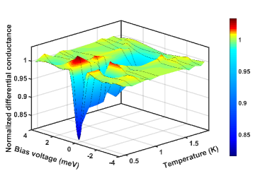
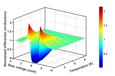
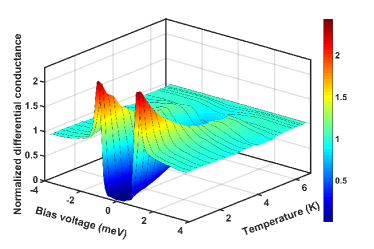
All curves were fitted according to the eq. (1) in order to obtain values of and . For the samples with MoGe thicknesses of 10 nm and 100 nm the results are plotted in Fig. 3. The broadening parameter does not exceed 0.1 meV. The results for 10 nm and 100 nm samples reveal a similar behavior with the critical temperatures 6.7 K, 6.6 K and superconducting gaps 1.02 meV, 1.05 meV, respectively. Due to the heavily smeared spectra of the 5 nm MoGe sample, it was impossible to fit them by eq. 1. Directly fom the Fig. 2 we estimated critical temperature for 5 nm MoGe as =1.9 K, where the ZBC is close to unity. The value of = 0.7 meV as a distance between coherence peaks was estimated as an upper limit. The superconducting coupling ratio values equal to 3.5 for the both 100 and 10 nm samples. This is very close to the values obtained on similar MoGe films by infrared spectroscopy Tashiro et al. (2008). In contrast, the 5 nm sample reveals a very high coupling ratio = 8.
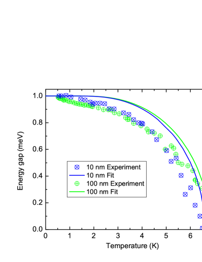
The temperature dependence of was compared with theoretical curve (lines in Fig. 3) according to the BCS model Abrikosov (1988):
| (3) |
where is the superconducting gap at zero temperature. One can see, that experimental data (dots) deviates from the theoretical prediction (lines). We suggest that such behavior could be explained by the influence of proximity effect.
Since the measurements were performed on the normal side of the metal-superconductor bilayer, the Andreev reflection Andreev (1964) would modify the local density of states. Instead of the true superconducting gap, the so-called minigap Belzig et al. (1996) would be obtained from the experiment. Due to difficulty of numerical analysis Belzig et al. (1996), in the current paper we perform only qualitative analysis of the experimental results. We can define two different coherence length. The first one is for superconducting layer and the second for adjacent normal Au overlayer:
| (4) |
where are the normal and superconducting coherence lengths, is the diffusive constant with is Fermi velocity, and is the elastic mean free path. In ref. Gupta et al. (2004) the normal coherence length on a similar bilayer Nb/Au has been estimated as =60 nm. The ratio of minigap to the real superconducting gap depends on and the thickness of the normal layer Belzig et al. (1996):
(a)
(b)
(c)
(d)
(e)
(f)
| (5) |
where is the thickness of normal metal. Taking as a true superconducting gap in bulk MoGe 1.13 meV Tashiro et al. (2008) and minigap from our experiments, we receive the ratio = 0.90. From Eq. (5) we receive the ratio = 0.08. It is in a good agreement with our experimental results =5 nm/60 nm = 0.08. Thus, for explanation of the superconducting gap in Au layer a proximity effect is sufficient. We can also conclude that down to 10 nm of MoGe films their superconducting properties are close to that of the bulk.
On 5 nm MoGe/Au bilayer the minigap is strongly suppressed. Also coherence peaks are almost absent and heavy ZBC present. Since is not changed in comparison to the 100 and 10 nm cases another pair breaking mechanism must operate to explain the observed spectra. At 5 nm MoGe thickness second interface is present above the STM junction, specifically superconductor - substrate interface. At this interface additional pair breaking effect - spin-flip scattering can be operational Belzig et al. (1996)) leading to a thin layer with suppressed superconducting parameters. This layer can affect the MoGe film via an inverse proximity effect and cause a strong smearing of the conductance spectra even at such low temperatures.
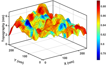
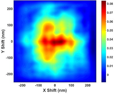
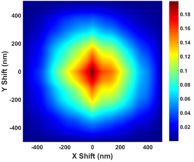
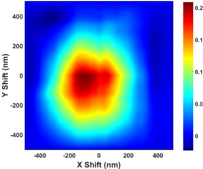
The ZBC maps obtained via current image tunneling spectroscopy are plotted in Fig 4 together with a topography of the Au overalayer. The -axis corresponds to the topography while colormap is the values of the ZBC (Fig. 4(a,c,e)). Such combination allows us to define the influence of the roughness of the surface on the superconducting properties. The two-dimensional cross-correlation between topography and ZBC was calculated for each sample (Fig. 4(b,d,f)). The relatively high central peak for 10 and 100 nm samples with the correlation value 0.2 indicate a good correlation between topography relief and ZBC. The hills of topography correspond to locally thicker gold film. Then, at these places the superconductivity would be slightly suppressed. In opposite, the pit parts have a thinner gold cover, and the lower values of ZBC is expected. It provide another evidence that in the 10 and 100 nm MoGe films the proximity effect is dominant.
On the contrary, the 5 nm MoGe sample shows the weakest correlation with a smeared central peak and the correlation value of only 0.08. It is despite the high RMS roughness which should impose a strong proximity effect. All this corroborates another pair-breaking mechanism, most probably the spin-flip scattering at the interface which is expanded by the the inverse proximity effect to the bilayer
IV Conclusions
Scanning tunneling microscopy and spectroscopy measured on 5 nm gold overalyer on 100, 10 and 5 nm MoGe films reveal suppression of superconducting energy gap and upon reduction of the thickness of MoGe films. The two-dimensional cross-correlation between topography and ZBC for the 10 and 100 nm MoGe samples indicates a proximity effect in Au layer where slightly smaller superconducting energy gap as compared to the bulk MoGe is observed. The superconducting properties of MoGe remain unchanged down to 10 nm thickness. In the STM LDOS spectra of the 5 nm MoGe sample a high ZBC and low coherence peaks are observed. This cannot be explained by a simple proximity effect and another mechanism is functioning. It is probably an inverse proximity effect from the interface between the MoGe film and the glass substrate where the spin-flip scattering suppresses the superconductivity.
V Acknowledgments
This paper is dedicated to Professor Viktor Valentinovich Eremenko on the occasion of his 85th birthday. Authors (A.F. and P.S) are very thankful to Prof. Eremenko for decades of fruitful collaboration. Viktor Valentinovich was and still is an excellent mentor in the field of magnetism for the whole Kosice Low Temperature Group.
This work was supported by projects APVV-0605-14, VEGA 1/0409/15 and U.S. Steel Košice.
References
- Anderson et al. (1979) P. W. Anderson, E. Abrahams, and T. V. Ramakrishnan, Phys. Rev. Lett. 43, 718 (1979).
- Altshuler et al. (1980) B. L. Altshuler, A. G. Aronov, and P. A. Lee, Phys. Rev. Lett. 44, 1288 (1980).
- Graybeal and Beasley (1984) J. M. Graybeal and M. R. Beasley, Phys. Rev. B 29, 4167 (1984).
- Strongin et al. (1970) M. Strongin, R. S. Thompson, O. F. Kammerer, and J. E. Crow, Phys. Rev. B 1, 1078 (1970).
- Haviland et al. (1989) D. B. Haviland, Y. Liu, and A. M. Goldman, Phys. Rev. Lett. 62, 2180 (1989).
- Szabó et al. (2016) P. Szabó, T. Samuely, V. Hašková, J. Kačmarčík, M. Žemlička, M. Grajcar, J. G. Rodrigo, and P. Samuely, Phys. Rev. B 93, 014505 (2016).
- De Gennes (1964) P. G. De Gennes, Rev. Mod. Phys. 36, 225 (1964).
- Belzig et al. (1996) W. Belzig, C. Bruder, and G. Schön, Phys. Rev. B 54, 9443 (1996).
- Samuely et al. (2013) T. Samuely, P. Szabó, Z. Pribulová, N. H. Sung, B. K. Cho, T. Klein, V. Cambel, J. G. Rodrigo, and P. Samuely, Superconductor Science and Technology 26, 015010 (2013).
- Agrait et al. (2003) N. Agrait, A. L. Yeyati, and J. M. van Ruitenbeek, Physics Reports 377, 81 (2003).
- Tinkham (2008) M. Tinkham, Introduction to Superconductivity, 2nd ed. (CBS Publishers and Distributors, 2008).
- Dynes et al. (1978) R. C. Dynes, V. Narayanamurti, and J. P. Garno, Phys. Rev. Lett. 41, 1509 (1978).
- Tashiro et al. (2008) H. Tashiro, J. M. Graybeal, D. B. Tanner, E. J. Nicol, J. P. Carbotte, and G. L. Carr, Phys. Rev. B 78, 014509 (2008).
- Abrikosov (1988) A. A. Abrikosov, Fundamentals of the Theory of Metals, 1st ed. (North Holland, 1988).
- Andreev (1964) A. F. Andreev, Sov. Phys. JETP 19, 1228 (1964).
- Gupta et al. (2004) A. K. Gupta, L. Crétinon, N. Moussy, B. Pannetier, and H. Courtois, Phys. Rev. B 69, 104514 (2004).