Simulation study of signal formation in position sensitive planar p-on-n silicon detectors after short range charge injection*
Abstract
Segmented silicon detectors (micropixel and microstrip) are the main type of detectors used in the inner trackers of Large Hadron Collider (LHC) experiments at CERN. Due to the high luminosity and eventual high fluence of energetic particles, detectors with fast response to fit the short shaping time of 20–25 ns and sufficient radiation hardness are required.
Charge collection measurements carried out at the Ioffe Institute have shown a reversal of the pulse polarity in the detector response to short-range charge injection. Since the measured negative signal is about 30-60% of the peak positive signal, the effect strongly reduces the CCE even in non-irradiated detectors. For further investigation of the phenomenon the measurements have been reproduced by TCAD simulations.
As for the measurements, the simulation study was applied for the p-on-n strip detectors similar in geometry to those developed for the ATLAS experiment and for the Ioffe Institute designed p-on-n strip detectors with each strip having a window in the metallization covering the p+ implant, allowing the generation of electron-hole pairs under the strip implant. Red laser scans across the strips and the interstrip gap with varying laser diameters and Si-SiO2 interface charge densities () were carried out. The results verify the experimentally observed negative response along the scan in the interstrip gap. When the laser spot is positioned on the strip p+ implant the negative response vanishes and the collected charge at the active strip increases respectively.
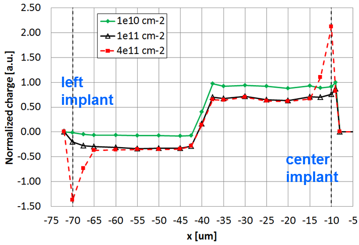
The simulation results offer a further insight and understanding of the influence of the oxide charge density in the signal formation. The main result of the study is that a threshold value of , that enables negligible losses of collected charges, is defined. The observed effects and details of the detector response for different charge injection positions are discussed in the context of Ramo’s theorem.
keywords:
Silicon radiation detectors; Strip sensors; Transient current; Charge collection; TCAD simulations1 Introduction
Segmented silicon detectors, like micropixel and microstrip, are the primary detector types used in inner trackers of the Large Hadron Collider (LHC) experiments [1, 2, 3]. Due to the high luminosity of the proton beam and the high counting rate the detectors with fast response to fit the short shaping time of 20–25 ns are required. The detectors must operate in a high-radiation environment for at least 10 years, maintaining a sufficient performance regardless of the accumulating degradation of the silicon properties.
The development and testing of advanced detectors include detailed studies of the detector current and charge responses using e.g. sub-nanosecond lasers, which enable to simulate the interaction of short or long range (MIP) particles with the detector. This gives information on the carrier transport in the detector bulk and the electric field distribution which are the input data for the prediction of the long-term scenario of the detector position sensitivity and charge collection efficiency (CCE) degradation. The latter is the governing parameter to define the guidelines of the detector operation after installation to the high energy physics experiments.
Earlier studies of silicon surface-barrier strip detectors have displayed a distinctive feature in the detector response - pulse responses of reversed polarity from the strips adjacent to the collecting strip, i.e. closest to the position of charge injection [4]. Later bipolar current pulse and negative charge signals from the adjacent strips were observed from non-irradiated planar Si strip detectors with a p-on-n structure [5, 6] where non-equilibrium carriers were generated via illumination of the detector strip side by a focused red laser pulse. The signals were recorded in the scanning mode and the negative charge signal reached up to 60% of the positive one [6]. The results were qualitatively explained by formation of a potential minimum under the Si-SiO2 interface due to the positive charge in the SiO2 layer. Evidently, potential distribution inside this minimum, which acts as a sink for collected electrons, depends on the interface properties thus affecting the charge losses.
The effect of the signal reversal has a potential to strongly influence the interpretation of the results on charge collection in the detector bulk damaged by irradiation and can be also sensitive to the radiation damage of the SiO2 layer and the interface. Recently the influence of these factors on charge and current signals was demonstrated in the study of radiation and environmental effects on silicon strip detectors [7, 8, 9]. It was shown that X-ray irradiation, biasing history and humidity led to reversal of the detector signal sign and incomplete charge collection and in a great extent affected the time of the signal relaxation to its steady-state value. Using numerical simulations, this effect was explained by a disturbance of steady state of the accumulation layer beneath the Si-SiO2 interface in the interstrip gap.
The results presented below continue the study described in [5, 6] with the goal to quantify the influence of the charge accumulated at the Si-SiO2 interface within the interstrip gap on the charge and current induction on the strips. This is performed via simulation using TCAD, which allows reconstructing the details of the potential and electric field distributions and the charge and current response of the strips. The results of the simulations are compared with the experimental data and their correlation is demonstrated. It is shown that there is a threshold interface charge density which initiates the appearance of reversed polarity signal at the neighboring strips and significant increase of charge losses at the readout strip.
2 Observations on charge induction in strip detectors
The main feature of silicon strip detectors performance studied here is the inversion of the charge signal on the strips neighboring to the one physically collecting the charge. The guideline for the charge signal inversion in strip detectors follows from the Ramo’s theorem [10]. It predicts the result of electrostatic induction produced by the moving charge in an arbitrary system of conductive electrodes placed in a non-conductive medium. According to the theorem, the charge generated by incident particles and drifting in the medium induces the current on any electrode as
| (1) |
or the charge
| (2) |
where is the drift velocity and the weighting electric field, the change of the charge Q induced on the readout electrode, and the change of the weighting potential . The weighting field is defined in the Ramo’s theorem as the electric field created by the unit potential () applied to the readout electrode while all the other electrodes of the device remain grounded ().
Transfer of a constant point charge created at some electrode (1) to the collecting electrode (2) will induce on the latter the full charge since
| (3) |
along any trajectory of the charge started at electrode (1) and ended at electrode (2). The shape of is defined by the charge trajectory and can be different. For example, the weighting field distribution for any p+ strip depends on the width of the strip, its pitch and the detector thickness. Thus, it reaches the maximum value at the strip due to a geometrical focusing effect. At the same time, the trajectory of drifting charge is defined by both the distribution of the space charge density and geometrical focusing effect. This can lead to the significant difference between the electric field lines governing the collected charge trajectory and the lines of weighting electric field.
Obviously, the current is induced on all non-collecting electrodes simultaneously. However, the weighting potential difference between the electrode (1) and any other electrode (different from the collecting one) equals zero, , and so does the induced charge, . This means that induced current arising during carrier drift has bipolar shape in which positive and negative current parts compensate each other. Evidently, this result also satisfies to the condition of charge conservation in the system of electrodes, i.e. the total charge induced on all electrodes is irrespective of the trajectory.
The result can be simply applied to the charge collection in silicon strip detectors with a surface-barrier or planar structure [11, 12, 13, 14]. They contain a non-conductive medium (space charge region (SCR)), and surface barrier or implanted p+ strips and the n+ back contact as conductive electrodes and the charge is collected via electron and hole drift inside the detector. The same logic as above predicts that only on the strip which physically collects the charge generated at any other strip or at the back contact the positive charge signal Q equals and a unipolar current response will be measured. All other strips show a bipolar current response and zero charge.
This statement is valid when the drifting charge is independent on time, i.e. there is no charge loss. Negative charge signal can be observed in the case of carrier trapping on defects or inside the potential minimum near the Si-SiO2 interface. In this case the charge on the collecting electrode will be smaller, i.e. and the positive and negative parts of the induced current do not compensate each other. Thus, the collected charge on the neighboring strips differs from zero and is negative.
Following these basic considerations, the experimental results in [5, 6] demonstrating the negative collected charge on the neighboring strips and the bipolar current responses were explained by carrier trapping only. The detectors used in [5, 6] were not irradiated and therefore carrier trapping in the bulk should be insignificant that speaks in favor of the proposed explanation based on the charge losses in the potential minimum near the detector surface in the interstrip gap [6].
3 TCAD simulation procedure and set-up
Due to their versatility and ability to reproduce not only generic behavior but also absolute values of measured silicon sensor characteristics before and after radiation, the Technology Computer-Aided Design (TCAD) numerical simulations have been applied as the next investigation tool in further studies of the reverse polarity charge signals. The reliability and accuracy of the TCAD simulations of the silicon strip detectors have already been documented in several publications and Ph.D. theses, including [7, 8, 15, 16, 17, 18, 19, 20] and [21, 22], respectively.
All simulations in this paper were carried out using the Synopsys Sentaurus111http://www.synopsys.com finite-element Technology Computer-Aided Design (TCAD) software framework. All presented simulations apply Neumann boundary and oxide-semiconductor jump conditions (potential jump across the material interface due to dipole layers of immobile charges), as well as Dirichlet boundary conditions for carrier densities and AC potential at Ohmic contacts that are used to excite the system.
For the simulation study of the observed charge collection behaviour in Refs. [5, 6] the 2-dimensional structures presented in figure 1 were applied. A two dimensional simulation was considered to be sufficient approach since, unlike for pixels, strip segmentation is monotonous along the second coordinate parallel to the sensor surface and provides no additional contribution to the local electric field evolution with voltage at the strip edges.
The physical thicknesses, pitches, strip widths and layer dimensions of the modelled strip sensor configurations are given in table 1. The comparison between experimental results and simulations were carried out on sensor designs in figures 1a and 1c with parameters as close to the real sensors as possible (AC-coupled strips, thickness 285 and resistivity 3–4 k for the ATLAS and DC-coupled strips, thickness 300 and resistivity 5 k for the Ioffe Institute design, respectively [5, 6]). For a simulation investigation focused on the differences in strip configurations, a modified ATLAS-design strip sensor structure (figure 1b and table 1), with equal physical thickness, strip coupling and interstrip gap to Ioffe Institute design, was applied. Also the bulk dopings of the two sensor substrates were set equal , that resulted in full depletion voltages well below 100 V. Lateral diffusion of the strip implant, that results in somewhat wider strip implant than its metallization when the two have equal nominal widths [5], was approximated by using Al width that left its edge 2 from the implant edge, as displayed in figures 1b and 1c.
The peak concentrations of both backplane n+ and strip p+ implantations were while both decayed to the bulk doping level within 1.0 depth using a gaussian profile. The area of the strip detectors used in measurements, 1010 mm2, was taken into account by stretching the 2-dimensional structures to the third dimension by an area factor.
As the density of the interface states observed in the Ioffe Institute-design strip sensors was typically in the range of and in ATLAS-design strip sensors about [1], these were included within the range of studied values at the Si-SiO2 interface.
All modelled sensors consisted of 3-strip structures, of which one strip close-ups are presented in figure 1. Illustrated in figure 1c is the Ioffe Institute design’s window in metallization of the p+ implant that allows the generation of electron-hole (e–h) pairs under the strip implant. The readout electrode was the centermost strip of the 3-strip sensor structure in all simulations. In the figures of section 4 it is always located at . The reverse bias voltage was provided from the backplane contact. In all designs each strip had a DC-coupled electrode at zero potential. For designs in figures 1b and 1c this was also the electrode used for charge collection, while for ATLAS-design in figure 1a charge collection was done by a capacitively coupled electrode separated from the silicon bulk by the oxide layer.
To generate charge carriers in the detector, a red laser with a wavelength of 670 nm and penetration of about 7 in silicon, was applied. The pulse length was set to 1 ns to match the experimental value in Refs. [5, 6]. With the intensity set to 20 W/cm2, this resulted in laser generated e–h pair density of about 345 . Two laser spot diameters were used in the simulations, a 10 which was also the diameter applied in the measurement set-up [5, 6, 23] and a 1 to enable scanning beyond experimentally available resolution. The red laser allows the investigation of a transient signal generated separately by the drift of electrons or holes (depending on which side of the detector is being illuminated) [24]. All laser scans were carried out at room temperature ().
| Sensor type | Thickness | Pitch | |||||
|---|---|---|---|---|---|---|---|
| [] | [] | [] | [] | [] | [] | [] | |
| ATLAS | 285.0 | 80.0 | 18.0 | 18.0 | 0.47 | 0.70 | 1.0 |
| Modified ATLAS | 300.0 | 80.0 | 20.0 | 16.0 | 0.47 | 0.70 | 1.0 |
| Ioffe Institute | 300.0 | 100.0 | 40.0 | 10.0 | 0.47 | 0.70 | 1.0 |


4 Simulation results
The simulated charge collection plots resulting from the red laser interstrip scans presented in this section, are always normalized to the maximum charge collected at the lowest value of Si-SiO2 interface charge density in each figure. This is to provide straightforward comparison of varied values of and laser diameter for the given strip sensor configuration.
Since the charges within the oxide layer interact with the active area of the silicon via the Si-SiO2 interface, as an effective approach their presence was modelled solely by the interface charge density (). Recombination throughout the silicon was implemented by recombination through deep defect levels in the bandgap, i.e. Shockley-Read-Hall (SRH) recombination [25], and band-to-band Auger recombination [26]. The doping dependence of SRH recombination resulted in non-uniform recombination lifetime distribution, reducing the recombination lifetimes from bulk values up to three orders of magnitude in the vicinity of heavily doped regions of strip implants and backplane blocking contact. The bulk recombination lifetimes, 100 ms for electrons and 10 ms for holes, were tuned according to an earlier study [16], where simulated carrier lifetimes were tuned to reproduce the measured low leakage currents of non-irradiated p-on-n detectors.
As stated above, TCAD package allows considering recombination in the silicon detector as a combination of SRH mechanism and Auger recombination. However, in the space charge region of the detector the SRH recombination is inefficient since a steady-state concentration of free carriers is negligible. Auger recombination can be neglected as well since the carrier concentration generated by laser pulses is too low. Therefore only carrier trapping can be a factor reducing the collected charge. However, this study was linked to the experiments performed on non-irradiated Si detectors where trapping in the detector bulk is negligible (typical trapping time is in the range of milliseconds leading to charge losses at the level of ratio , where is the charge collection time and is the carrier trapping time).
The surface recombination was estimated based on the results of [7] where it was shown that the density of surface traps in the interstrip gap of non-irradiated silicon sensor is about two orders of magnitude lower than the interface charge density. Thus, for the density of surface traps should be in the order of . Estimation of the surface recombination velocity using a rather large capture cross-section of surface trapping centers of and thermal velocity at room temperature of [24] gives the value of 200 cm/s. Since this value does not affect the accuracy of the treatment of the experimental data used in this study, for simplicity the simulations presented below do not consider the surface SRH recombination.
Since the oxide and interface charges depend on the silicon wafer orientation, being larger for wafers [27], in the simulation the interface charge was varied within covering the range for both and orientations [1, 6, 7, 28].
4.1 Interstrip scans with 10 diameter red laser
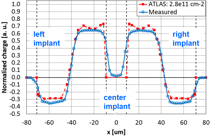
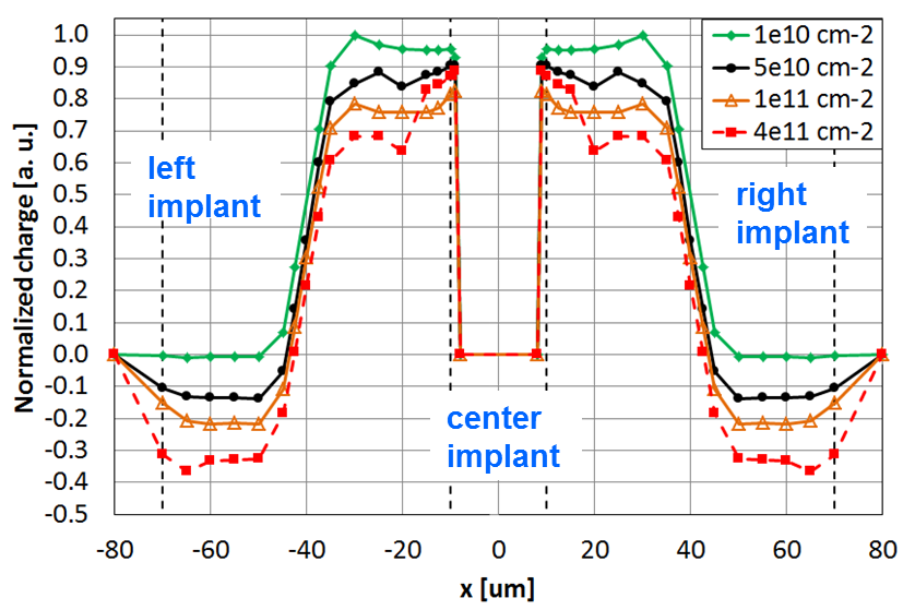
Simulation results for the cross strip scans of a strip detector with ATLAS design from the p+-strip side show that the collected charge correlates well with the topology of the strips and the 80 pitch is clearly recognizable, as can be seen from figure 2. When the laser position is either at the ’center implant’, which is considered as the readout strip, or its adjacent strips, the resulting plots for the collected charge () contain low signal regions due to the opacity of the strip implant wide metallization. The simulated laser produces optical carrier generation that has parallel to the sensor surface a Gaussian distribution within 10 . Thus, if the peak value of optical carrier generation is minimized by the Al layer, also the tails of the distribution are minimized. This leads to step function-like behavior of the simulated charge collection curves at the edge of the strip metallization that is not seen in the measured curve in figure 2a.
As in earlier measurements [5, 6], a significant reversed polarity signal is observed when the point of carrier injection is beyond midgap distance from the readout strip, i.e. when in figure 2. The reverse polarity signal around and the positive signals between for are within 6% and 2–7%, respectively, from the corresponding measured values, as shown in figure 2a. The measured location of polarity reversal and the slope of the charge collection curve around midgap are closely reproduced by the simulation.
The normalization of the measured charge collection curve in figure 2a was carried out so, that the sum of the absolute maximum values of the positive and negative polarity charges would be equal to one. As can be seen from figure 2b, this is also the consequence of normalization to the maximal simulated collected charge for the lowest value of that has negligible contribution from the reverse polarity signals (and thus, undiminished positive polarity signals at distances less than midgap from the collecting strip). These approaches enable reliable comparison between the measured and simulated charge collection curves.
The charge collection scans display a strong dependence on interface charge density . When midgap from the centermost strip in figure 2b, the highest value of corresponds to the highest negative collected charge. However, the effect essentially vanishes at the lowest value of . When midgap, reversed behavior is observed, the highest now corresponds to the lowest positive collected charge until the implant edge is reached. The two highest value plots also present sensitivity to the strip implant edges. The electric field peaks at the implant edges react strongly to the increase of and start to amplify charges, both positive and negative, injected at their position. This is especially apparent for the highest value , which around 5 from the implant edge of the collecting strip surpasses in charge collection the curve and converges with the charge collection results of . More detailed investigation of the effects of charge multiplication after a charge injection at the implant edge follows in section 4.3.
When the simulations were repeated for an otherwise identical strip sensor structure but with either DC- (direct contact to strip implant) or capacitively-coupled (oxide layer between the strip implant and collecting contact) charge collection electrodes, the results of red laser scans were within 2.5% at any laser position, thus displaying an essentially coupling independent behavior.
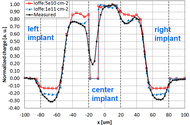
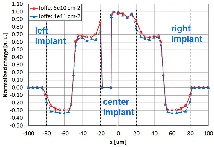
The corresponding measured and simulated red laser scans of a detector with Ioffe Institute design are presented in figure 3. The scans are now carried out across the strips with implant width of 40 but with metallization of only 10 , as presented in figure 1c. Scan results in the SiO2 layer region and at the strip impants adjacent to the readout strip at the center show similar behavior to the ATLAS-design sensor results in figure 2, while the drop of the signal from centermost strip now occurs only within the area of the metallization window of the p+ implant.
As seen in figure 3, both in measurement and simulation the maximum collected charges are observed in the area free from the metal contact at the centermost implant ( coordinates between -20–20 ). The normalization of both experimental and simulated curves is now done by setting the highest charge collected at the implant’s metallization window, where no charge losses occur, equal to one. Complete charge collection at the metallization window is also reflected in independent collection of the simulated charges, which is shown in greater detail in figure 6b. The amplitudes of the positive signals collected in the area of the oxide, with laser distance from the readout strip less than midgap, move from about 87% to 74% with increased values of , while the negative signals at the region beyond the midgap from the collecting strip for different values of vary between 13%–22% of the maximal positive signal. The simulated charge collection curves for the higher value of are in close agreement with measured results at distances less or equal to midgap from the collecting strip, while the reversed polarity signals around are within 7–10% from measured values.
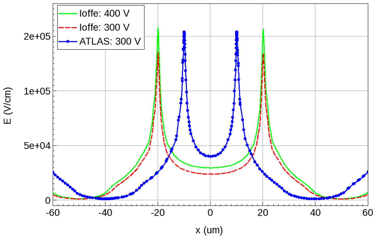
When the charge collection plots of equal values in figures 2b and 3 are compared, the two sensor designs display no significant differences at the strip implant edges. Thus, the doubled strip implant width, while maintaining equal interstrip gap size, of the Ioffe Institute-design sensor that results in lower average electric fields in the area of the strip implant for the given biasing voltages, presented in figure 4, has negligible effect on charge collection at the implant edge. Also the amplitudes of negative signals in the two figures match closely.
As the figures 2a and 3 demonstrate, the simulated red laser scans with diameter matching the experimental set-up reproduce reasonably well the measured charge collection behavior of the ATLAS- and Ioffe Institute-design strip detectors.
4.2 Interstrip scans with reduced red laser diameter
For higher resolution study of the dependence of the collected charge on the interface states , observed in section 4.1, the scans were next repeated with reduced laser diameters between 1–3 , with 670 nm wavelength. Initial simulations with 1 diameter laser proved to be problematic when laser position was at the collecting strip either at the strip-side of an implant bare from metallization, as in figures 6a and 6b, or at the backplane as in figure 9. The complex calculations of the doping dependent SRH recombination in the region of high doping gradients resulted in unstable charge collection at the strip implant that was not redeemed by significantly increased mesh density in the modelled structure. This approach also increased the CPU time of each simulated charge injection point exponentially (e.g. mesh density increase by a factor of 3.5 leads to over 20 times longer simulation time), which is undesirable when the simulation study includes several hundred data points. However, increase of laser diameter from 1 to 3 stabilized the simulated charge collection at high doping gradient regions considerably, while still providing substantially increased resolution to the charge injections of section 4.1. Thus, in aforementioned cases the following charge collection results were achieved by 3 diameter laser illuminations.
The scan results for modified ATLAS-design strip detector in figure 5 are now significantly different to figure 2b and reveal new features of the charge collection behavior between strips. As displayed in figure 5 the charge collection of the highest value is amplified substantially at the implant edges due to small spatial spread of the laser that results in the charge injection to be focused at the position of the electric field maxima.
Also in figure 5 it can be seen that the polarity reversal of the signal at midgap takes place abrubtly, within 5 . When the laser spot is above the oxide the two highest values of are now collecting almost equal amount of charge before the edges of the interstrip gap. Finally, it can be observed from figure 5 that the effect of reversed polarity signals for laser positions beyond midgap from the readout strip is still present also for the lowest value of .
The laser scan results, with decreased laser diameter, of the Ioffe Institute-design strip sensor in figure 6 also display new features in charge collection behavior with respect to figure 3. The negative polarity signals in figure 6a between adjacent and centermost strips at around are now incresed by about 17% and 12.5% for values and , respectively. The charge collection at the lower value of now reproduces closely the amplitudes of the measured reverse polarity signals in figure 3. As for the modified ATLAS-design, the polarity reversal at midgap is significantly more abrupt than in figure 3, taking place within 5 .
The amplitudes of the positive signals collected in the area of the oxide, with laser distance from the readout strip less than midgap, are also considerably lower, moving from about 70% to 65% with increased values of . For both values of , the positive signal collected at oxide reaches a local maximum close to midgap, immediately before polarity reversal, due to the high potential gradient close to the interstrip midgap potential maximum that increases the carrier drift velocities.
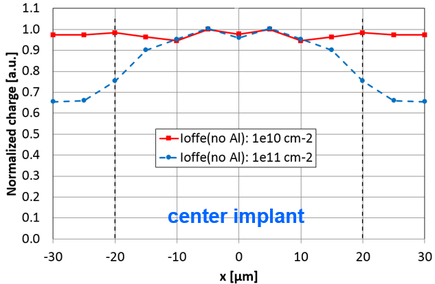
The charge collection plots in figure 6a at the centermost strip have a dependence when the laser spot is getting closer to the right edge of the implant, free of metallization. To further investigate the dependence when the laser spot is over the strip implant, the scans at the readout strip were repeated without any metallization. The results in figure 6b show that the charge collection of lower fluctuates within 5% with no descending pattern towards and beyond the implant edge. However, the curve for higher has a descending shape towards the implant edge with about 25% lower charge collected at the edge than for lower value of . The charge collection of the two values essentially converges within 10 from the implant edge towards its center. Thus, the differences in at the interstrip gap also affect the charge collection of a charge injection done over the implant (with strip metallization removed) up to few microns from the implant edge.
4.2.1 Critical interface charge density
The strong dependence of the reversed polarity signals, collected beyond midgap from the readout strip, on Si-SiO2 interface charge density is seen clearly in the plots of sections 4.1 and 4.2. This poses a question, is it possible to find a threshold level of beyond which the effect of negative polarity signals vanishes.
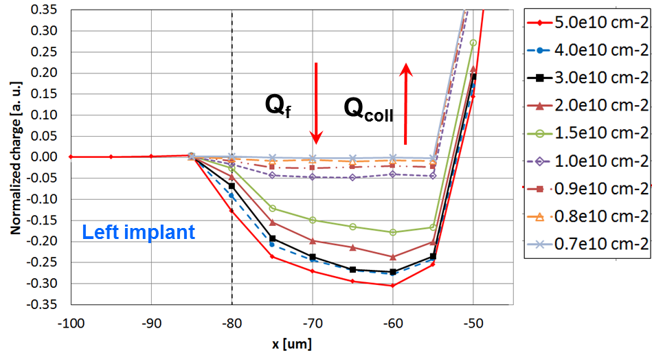
The iteration of values between , for laser scans of a Ioffe Institute-design sensor in the region of the interstrip gap where negative polarity signals appear, is presented in figure 7. As can be seen, the negative charge collected at the centermost strip has a strong dependence on and moves towards zero with decreased values. When the collected charges at , where their amplitude is at maximum in figure 7, are plotted as a function of in figure 8, three regions can be extracted. First, a region where negative signals settle to zero at , then a strongly dynamic region of negative signal increase between , and ultimately a region with significantly reduced increase of the negative signal (about 23% of the dynamic region) for higher values of .
When the recombination lifetimes are varied from the initial values (presented in the beginning of section 4) to very short and very long, respectively, the results seen in figure 8 remain essentially the same. This can be expected since the ratio reflecting the level of trapping related charge losses (discussed at the start of this section) is still only for the shortest recombination lifetime of electrons.
Thus, the negative polarity signals display an exclusive dependence on Si-SiO2 interface charge states for a short range charge injection from the stripside at a given voltage and bulk doping. The interstrip resistances remain at several tens of G throughout the studied range, which is in vicinity of experimentally observed values [16]. Optimization of does not then compromise the strip isolation, which in segmented p-on-n sensors is not a critical parameter since positive charges at the Si-SiO2 interface do not attract holes (that could potentially open a conductive channel between the strips) to the accumulation layer.
4.3 Interstrip scans from the backplane
The red laser scans of the unsegmented n+-side of an Ioffe Institute-design strip sensor were enabled by removing the metallization from the backplane of the modelled structure. The absence of the reversed polarity signals observed in earlier measurements [5] is reproduced by the simulation, as seen in figure 9. No dependence on is observed when the laser is moving below interstrip gap. The increase of charge sharing between the two strips in figure 9 as a function of laser diameter is also obvious.
The stability of the charge collection simulation at the collecting strip also increases with laser diameter, as discussed in the beginning of section 4.2. By doubling the diameter from 1 the charge collection dip at the edge of the collecting strip moves from 10% to 4%, while for 3 diameter and above no fluctuations in the region of the collecting strip implant are observed and the curve shapes converge with measured data in Ref. [5].
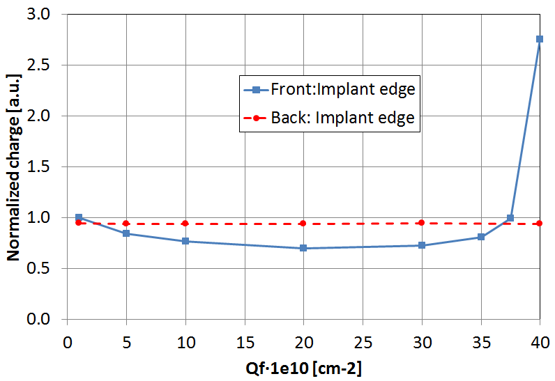
To further investigate the dependencies of the charge collection behavior after red laser backplane illumination in the vicinity of the readout strip, the laser position was fixed to the implant edge ( in figure 9) and charge collection was monitored as a function of , as shown in figure 10. As can be seen, for comparison the charge injection was also repeated from the strip-side. The range was set wide enough to include experimentally observed values [1, 6].
When the laser is at the strip-side in figure 10, a clear charge multiplication (CM) effect is seen at . At values below this, increased results in significantly decreased positive collected charges due to increasing negative contribution from electron drift along the surface of the interstrip gap. The increase of increases also the electric field peaks at the implant edges. After the threshold value mentioned above this leads to CM of charge carriers that with further increase of fully compensate for the decreased collected charge. However, when charge injection is done from backplane, the collected charge is completely independent from and no CM is seen. Thus, when no physical processes account for the charge collection fluctuations of the 1 red laser curves in figure 9 and since these vanish at increased laser diameter charge injections, the behavior can be deemed as simulators sensitivity to charge injections with very small spatial spread in the vicinity of high doping gradients, as discussed in the beginning of section 4.2.
4.4 Transient signals
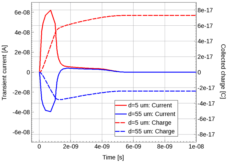
To investigate the time evolution of the transient signals induced by the red laser, two laser spot positions were considered, 5 from the edge of the readout strip and 5 from the edge of its adjacent strip ( in figure 6a, respectively). These positions enable the study of transient currents leading to both positive and negative collected charges in the case of short range charge injection from the strip-side. Since the current response is
| (4) |
the features of the collected charge distribution as a function of position, presented in the previous sections, can also be seen in the transient current plots.
The current pulses in a red laser illuminated Ioffe Institute-design strip sensor at in figure 11 show that the duration of the negative current response is identical to the width of the positive current response. Also distinct is the smaller amplitude of the negative current pulse when . Both pulses induced by the electron drift have identical low-amplitude positive tail that goes to zero after 5 ns. As can be seen from the time integrals of the transient currents, i.e. induced charges, this results in the reduction of the negative charge until the charge collection is complete.
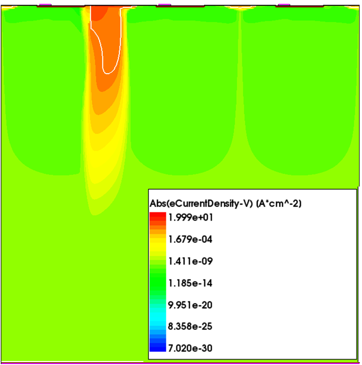
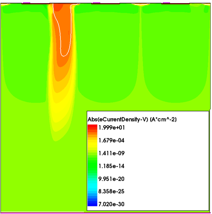
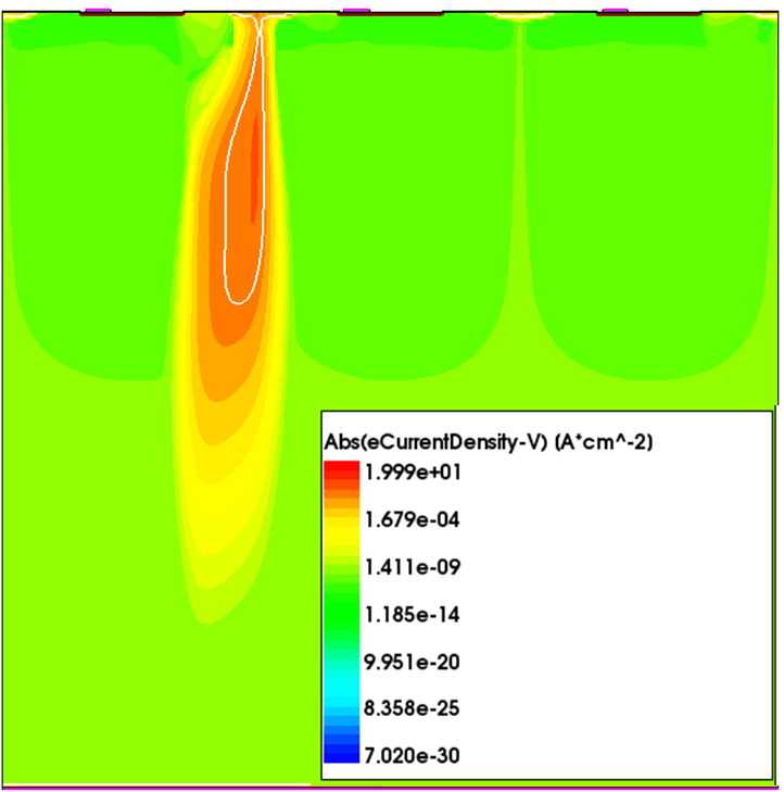
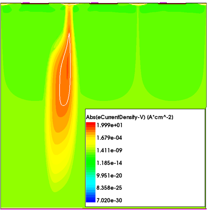
Since the polarity reversal of the transient current signal for in figure 11 takes place at , the time evolution of electron current densities before and after this point were plotted in figure 12 as being the most revealing interval for understanding the formation of the transient signals. As the charge injection point in figure 12 is from the centermost strip ( from the leftmost strip) the two transient signals in figure 11 can be considered to be simultaneously induced at the two adjacent strips from this charge injection position.
Figures 12a and 12b show that before the polarity reversal of the negative transient signal in figure 11 the highest electron current densities are seen between the leftmost strip closest to the charge injection point and the midgap between the leftmost and center strips of the 3-strip sensor structure. The induced negative transient signal at the centermost strip is then solely generated by the electron drift from the potential minimum of the leftmost strip to the local potential maximum at the midgap, while the positive transient signal seen at the leftmost strip is a composite of electron drift toward global and local potential maxima at the sensor backplane and midgap, respectively. The transient signal at the leftmost strip is then the result of positive signal induced from drift towards the sensor backplane reduced by opposite sign signal induced from the drift parallel to the sensor surface having equal amplitude to the transient signal seen at the centermost strip.
From figures 12c and 12d it can be seen that the polarity reversal from negative to positive in figure 11 is the result of completed electron drift parallel to the sensor surface to the local potential maximum at the midgap. After this, i.e. at , only electron current densities normal to the sensor surface are observed. Since these are generated essentially from the electron drift at equidistance from the leftmost and center strips, the induced transient signals at both strips have identical sign and amplitude.
5 Discussion
To provide an interpretation of the observed results in this study, it is considered that when the readout contact is a cathode, as in p-on-n strip sensors, holes drifting towards it and electrons drifting away from it induce a positive transient current that accumulates a positive collected charge. Reversed directions result in reversed polarity charge signals.
These statements are just consequences of the Ramo’s theorem [29, 30], which gives an accurate result for the induced current, that is the charge induction rate, as
| (5) |
where is the carrier charge with as the elementary charge, is the weighting electric field and is the charge drift velocity.
-
1.
The reduction of the laser diameter from the experimentally used value [5, 6] to 1–3 in figures 2 and 5 for modified ATLAS-design as well as in figures 3, 6a and 9 for Ioffe Institute-design, lead to several times smaller averaging of the effects to the carrier transport from the electric field distribution and drift distances parallel to the sensor surface. This is seen in figures 5 and 6a in the decrease of positive collected charges and increase of the absolute value of the negative polarity charges when the laser spot position was moved across the interstrip oxide, as well as sharper polarity reversal at the midgap and higher sensitivity to the edges of the strip implants.
-
2.
The effects of smaller diameter laser spot also include a visible reduction of the dependence, i.e. the charges collected from laser illumination over the interstrip oxide have decreasing differences with increased . Evidence from figures 2b, 5 and 8 indicates that for the smaller diameter charge injection there is an upper threshold value of beyond which only limited increase in negative polarity signals is seen with increased in the lower field regions of the interstrip gap.
-
3.
Figure 6b displays the dependence of the collected charge when the laser spot is moved over the readout strip implant close to its edge when the strip metallization has been removed. The order of magnitude difference in for the two curves results in about 25% lower collected charge for the higher at the edge of the strip implant while the dependence essentially vanishes when the 3 diameter laser spot is moved 10 from the implant edge towards its center.
-
4.
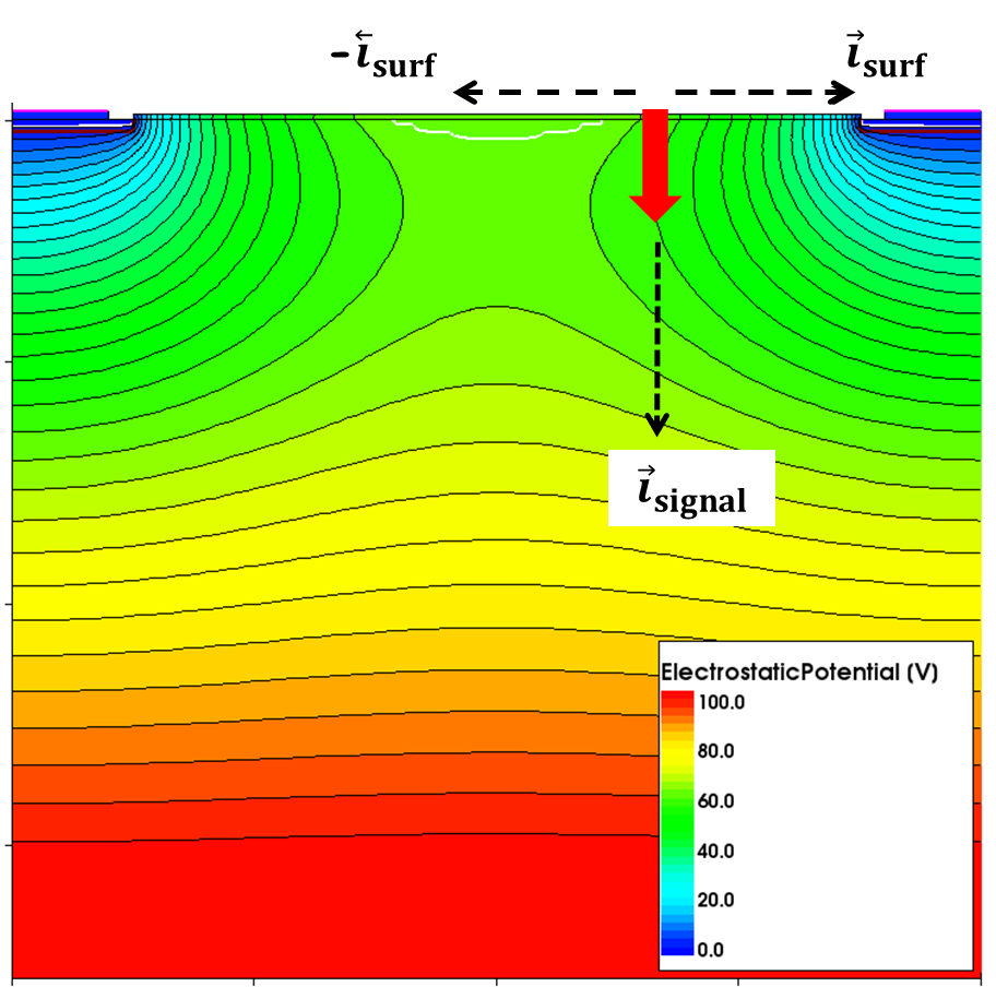
The interpretation of earlier experimental observations concluded that the oxide layer with the attractive electric field may be considered as a "sink" for electrons that are moving close to the surface with the probability to reach the surface and be trapped in the interstrip gap significantly higher than for those, which are generated under the p+ implant [6]. Since substantial reduction of the collected charge is observed at laser positions less than midgap distance from the collecting strip, the total transient current signal can be considered as a composite of the currents induced by the carrier drifts along the surface () and orthogonal to the surface through the sensor thickness () as
(6) These are illustrated in figure 13a. With the statements from the first paragraph of this section and equation (6) the curves in figure 6b can now be interpreted of having minimal contribution from the opposite sign to in the middle of the p+ implant, while its share increases when the point of charge injection moves to the implant edge, i.e. when the electron drift along the surface of the interstrip gap changes from negligible to significant.
If is broken into two components with opposite velocity vectors, as in figure 13a, the increase in collected charges close to midgap in figures 5 and 6a can be interpreted to be the result of the components compensating each other with close to equal amplitudes. As a result, in the middle of the interstrip gap has decreased contribution from . When the position of charge injection moves closer to the implant edge of the collecting contact, the two opposite components of become increasingly non-equal, leading to growing opposite sign contribution to .
-
5.
The strip-side red laser illuminations at the implant edge of the collecting strip in figure 10 show strong dependence on . Due to the charge injection position, the only possible direction for is away from the collecting strip. Thus, even though both and are now induced from the drift away from the collecting contact, towards the adjacent strip and towards backplane, they clearly induce opposite polarity signals. Hence, as in the above interpretation of compensation of the two components of , the equal sign charge carriers with different direction velocity vectors compensate each other.
-
6.
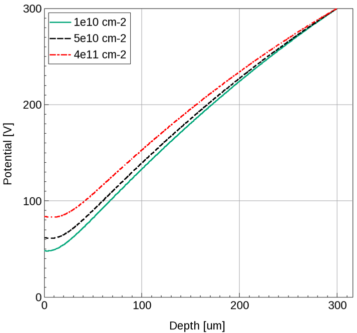
Following the model proposed in [6] the curvature of the electric field under SiO2 in interstrip gap has a minimal potential for electrons at the interface and a saddle point with local potential maximum at certain distance in the bulk. Such a potential distribution can act as sink for the electrons. Undoubtedly the local potential maximum seen in figures 13a and 13b works against the drift of the electron cloud to the interface, however, some fraction of the cloud can diffuse towards the interface via the potential minimum. Obviously the shape of the peak is important for the charge losses and the shape changes with , as can be seen from figure 13b.
The influence of sinks to the charge collection can also be concluded from figure 11. The transient current curve for (5 from the strip adjacent to the readout strip) displays first a higher amplitude negative polarity signal due to electron drift from the high electric field region, repulsed by the injected electrons, towards the readout strip. Then a low amplitude positive ’tail’ is induced due to the drift of the electrons, not trapped at the potential minimum, away from the readout strip towards the sensor backplane. Identical ’tail’ is observed for transient curve in figure 11, showing that the accumulation layer electrons are again repulsed to the local potential maximum region providing the low amplitude, slow component to the positive transient signal.
-
7.
As was shown in figures 7 and 8, it is possible to find values of Si-SiO2 interface charge density within an order of magnitude of typical values seen in non-irradiated strip sensors ( [1, 6, 7, 28]) that can reduce negative to an insignificant level in a p-on-n strip sensor. In the particular cases of ATLAS and alternative Ioffe Institute topologies with different strip pitches and strip implant widths the values are in the range of .
-
8.
The resulting observations lead to the conclusion, that a charge injection through Si-SiO2 accumulation layer of a segmented p-on-n silicon sensor induces of which sign is always opposite relative to . The level of influence from to is governed by the localization in the potential minimum originated from at Si-SiO2 interface that manifests as an imbalance between the two opposing components of induced by the drifts parallel and normal to the sensor surface.
6 Conclusions
The performed simulations of the influence of Si-SiO2 interface charge on the current response and charge collection efficiency reproduces all experimental features, i.e. negative fraction in the charge response and tens of percents reduction of CCE which were observed earlier [5, 6] in non-irradiated Si strip detectors. When agreement between measurement and simulation was obvious the simulations could be extended to parameter values beyond the experimental study with justified confidence on the results. The study demonstrated that:
-
1.
Variation of the interface charge and its influence on the detector response in the performed modelling gives clear indication that the features are originated from the interface charge and are defined by its density.
-
2.
There is a critical density of the interface charge which initiates the features and the value of critical density is not sensitive to the topology of the strip detector.
-
3.
The critical interstrip charge density was defined and in the particular cases of ATLAS and alternative Ioffe Institute topologies, with different strip pitches and strip implant widths, the values are in the range of .
-
4.
Simulation of the charge collection in the interstrip gap with the laser beam spot equal to that used in the experiment (10 diameter) or several times less showed that the negative response in the active strip changes sharply its value in the middle of the interstrip gap. This shows a direct link to the trajectory of the collected charge cloud. It is important to which strip the electric field line and the related trajectory of the cloud flow.
The performed study is a physical base for explanation and prediction of the influence of radiation on the detector performance. Generation of the charge at the Si-SiO2 interface is a specific process sensitive to the properties of SiO2 layer and its thickness. The results show the possibility for the irradiation effect stabilization and/or its minimization via optimization of interstrip gap passivation.
The results provide grounds to extend the study to the experimentally observed absence of reversed polarity signals in infra-red laser (with minimum ionizing particle-like carrier generation) illuminated strip sensors [5], as well as the possible sensitivity of n-on-p strip sensors to the effect, which is a strict plan for the nearest future.
References
- [1] D. Robinson, et al., Silicon microstrip detectors for the ATLAS SCT, Nucl. Instr. Meth. A 485 (2002) 84–88. doi:10.1016/S0168-9002(02)00536-3.
- [2] L. Andricek, et al., Design and test of radiation hard p+n silicon strip detectors for the ATLAS SCT, Nucl. Instr. Meth. A 439 (2000) 427–441. doi:10.1016/S0168-9002(99)00901-8.
- [3] P. P. Allport, et al., A comparison of the performance of irradiated p-in-n and n-in-n silicon microstrip detectors read out with fast binary electronics, Nucl. Instr. Meth. A 450 (2000) 297–306. doi:10.1016/S0168-9002(00)00259-X.
- [4] H. W. Kraner, et al., Charge Collection in Silicon Strip Detectors, IEEE Trans. Nucl. Sci 30 (1983) 405–414. doi:10.1109/TNS.1983.4332300.
- [5] V. Eremin, J. Bohm, S. Roe, G. Ruggiero, P. Weilhammer, The charge collection in single side silicon microstrip detectors, Nucl. Instr. Meth. A 500 (2003) 121–132. doi:10.1016/S0168-9002(03)00330-9.
- [6] E. Verbitskaya, et al., Effect of SiO2 Passivating Layer in Segmented Silicon Planar Detectors on the Detector Response, IEEE Trans. Nucl. Sci 52 (2005) 1877–1881. doi:10.1109/TNS.2005.856907.
- [7] T. Poehlsen, et al., Charge losses in segmented silicon sensors at the Si-SiO2 interface, Nucl. Instr. Meth. A 700 (2013) 22–39. doi:10.1016/j.nima.2012.10.063.
- [8] T. Poehlsen, et al., Study of the accumulation layer and charge losses at the Si-SiO2 interface in p+n-silicon strip sensors, Nucl. Instr. Meth. A 721 (2013) 26–34. doi:10.1016/j.nima.2013.04.026.
- [9] T. Poehlsen, et al., Time dependence of charge losses at the Si-SiO2 interface in p+n-silicon strip sensors, Nucl. Instr. Meth. A 731 (2013) 172–176. doi:10.1016/j.nima.2013.03.035.
- [10] S. Ramo, Currents induced by electron motion, Proc. I.R.E. 27 (1939) 584–585. doi:10.1109/JRPROC.1939.228757.
- [11] V. Radeka, Low-Noise Techniques in Detectors, Annu. Rev. Nucl. Part. Sci. 38 (1988) 217–277. doi:10.1146/annurev.ns.38.120188.001245.
- [12] G. Lutz, Semiconductor Radiation Detectors, Springer, Berlin, 1999.
- [13] Z. He, Review of the Shockley-Ramo theorem and its application in semiconductor gamma-ray detectors, Nucl. Instr. Meth. A 463 (2001) 250–267. doi:10.1016/S0168-9002(01)00223-6.
- [14] H. Spieler, Semiconductor Detector Systems, Oxford University Press, New York, NY, USA, 2005.
- [15] T. Peltola, Charge collection efficiency simulations of irradiated silicon strip detectors, JINST 9 (2014) C12010. doi:10.1088/1748-0221/9/12/C12010.
- [16] A. Bhardwaj, R. Dalal, R. Eber, T. Eichhorn, K. Lalwani, A. Messineo, T. Peltola, M. Printz, K. Ranjan, Simulation of Silicon Devices for the CMS Phase II Tracker Upgrade, Compact Muon Solenoid, CMS DN -2014/016 (2015).
- [17] T. Peltola, et al., A method to simulate the observed surface properties of proton irradiated silicon strip sensors, JINST 10 (2015) C04025. doi:10.1088/1748-0221/10/04/C04025.
-
[18]
T. Peltola,
Simulation of radiation-induced defects, PoS 031 (2015) (VERTEX2015).
URL pos.sissa.it/archive/conferences/254/031/VERTEX2015_031%.pdf - [19] T. Peltola, et al., Characterization of thin p-on-p radiation detectors with active edges, Nucl. Instr. Meth. A 813 (2016) 139–146. doi:10.1016/j.nima.2016.01.016.
-
[20]
R. Dalal, et al., Simulation of irradiated Si
detectors, PoS 030 (2014) (VERTEX2014).
URL pos.sissa.it/ -
[21]
R. Eber,
Investigations of new sensor designs and development of an
effective radiation damage model for the simulation of highly irradiated
silicon particle detectors, Ph.D. thesis, Karlsruhe Institute of Technology
(2013).
URL http://ekp-invenio.physik.uni-karlsruhe.de/record/48328%/files/EKP-2014-00012.pdf -
[22]
T. Peltola,
Numerical simulations of semiconductor radiation detectors for
high-energy physics and spectroscopy applications, Ph.D. thesis, University
of Helsinki (2016).
URL https://helda.helsinki.fi/bitstream/handle/10138/159441%/numerica.pdf?sequence=1 - [23] G. Ruggiero, Signal Generation in highly irradiated silicon microstrip detectors for the ATLAS experiment, Ph.D. thesis, Dept. Phys. Astr., University of Glasgow, Glasgow, U.K. (2003).
- [24] S. M. Sze, Physics of Semiconductor Devices, 2nd Edition, John Wiley & Sons, New Jersey, 1981.
- [25] W. Shockley, W. T. Read, Jr., Statistics of the recombinations of holes and electrons, Phys. Rev. 87. doi:10.1103/PhysRev.87.835.
- [26] E. H. S. Burhop, The Auger Effect and Other Radiationless Transitions, Cambridge Monographs on Physics, Cambridge, 1952.
-
[27]
J. Zhang, et al., X-ray induced radiation damage in
segmented p+n silicon sensors, PoS 019 (2012) (VERTEX2012).
URL pos.sissa.it/ - [28] F. Moscatelli, et al., Combined bulk and surface radiation damage effects at very high fluences in silicon detectors: Measurements and TCAD simulations, IEEE Trans. Nucl. Sci 63 (2016) 2716–2723. doi:10.1109/TNS.2016.2599560.
- [29] G. Cavalleri, E. Gatti, G. Fabri, V. Svelto, Extension of Ramo’s theorem as applied to induced charge in semiconductor detectors, Nucl. Instr. Meth. A 92 (1971) 137–140. doi:10.1016/0029-554X(71)90235-7.
- [30] E. Gatti, G. Padovini, V. Radeka, Signal evaluation in multielectrode radiation detectors by means of a time dependent weighting vector, Nucl. Instr. Meth. A 193 (1982) 651–653. doi:10.1016/0029-554X(82)90265-8.