A high-resolution programmable Vernier delay generator based on carry chains in FPGA
Abstract
This paper presents an architecture of high-resolution delay generator implemented in a single field programmable gate array (FPGA) chip by exploiting the method of utilizing dedicated carry chains. It serves as the core component in various physical instruments. The proposed delay generator contains the coarse delay step and the fine delay step to guarantee both large dynamic range and high resolution. The carry chains are organized in the Vernier delay loop style to fulfill the fine delay step with high precision and high linearity. The delay generator was implemented in the EP3SE110F1152I3 Stratix III device from Altera on a self-designed test board. Test results show the obtained resolution is 38.6 ps, and the differential nonlinearity (DNL) \ integral nonlinearity (INL) is in the range of (-0.18 least significant bit (LSB), 0.24 LSB) \ (-0.02 LSB, 0.01 LSB) under the nominal supply voltage of 1100 mV and environmental temperature of 20 ∘C. The delay generator is also rather resource cost efficient which uses only 668 LUTs and 146 registers in total.
I Introduction
Highly accurate programmable delay generator is used to generate an expected time interval between two successive pulses. It is manifested as core component in many physical instruments, for example in the positron emission tomography (PET) system YLiu2003 , in the STACEE gamma-ray astrophysics experiment JPMartin2000 and in the conflict detector applications for multi-synchronous systems RGinosar2011 . Besides, precise delay generator is very beneficial for any timing experiments and tests HUJang-RSI ,JKalisz-RSI .
Generally speaking delay generators can be divided into two classifications: absolute delay generators and relative generators. Absolute generators directly produce a delayed output signal relative to the input trigger signal which usually contains an inevitable intrinsic fixed delay making the delay result less accurate. Relative generators produce two new delay outputs between which the time interval equals the programmed delay amount after an effective detection of the input trigger signal. Relative generators can achieve much higher accuracy and are the main concerns in this paper. However absolute delay generators may be necessarily required under some circumstances, even so relative delay generators can also be applied to these cases by making proper adjustment of the utilization manner of the output delay signals. If this is applicable, the leading delay output of the relative delay generator acts as the new time base or effective trigger signal instead of the actual input trigger signal.
In this paper we focus on the designing of precise delay generators by utilizing the field programmable gate array (FPGA) chip, which is widely adopted in many scientific instruments mainly benefiting from its real-time signal controlling and processing ability and flexible reconfigurability. Y. Song proposed an FPGA-based delay generator with 65 ps resolution and 400 ps RMS jitter. However the delay was not fully generated by a single FPGA chip and needed to be calibrated by an extra fine delay chip AD9501 YSong2011 . R.Giordano proposed a high-resolution synthesizable delay line in a Xilinx Kintex-7 FPGA with 11 ps resolution and 3.0 ns delay range RGiordano2015 . It opened up a new way to build high-performance delay line without any custom design intervene.
The dedicated carry chains, which are especially designed to implement fast arithmetic functions such as adders, counters and comparators, are important components of modern FPGAs. Since the propagation delay between two consecutive basic elements along the carry chain is rather small, it has the promise to fulfill the delay generating task accurately. Many time-to-digital (TDC) KeCui_TDC2017 -WangYG_TDC2016 converter designs, which in function can be seen as the reversion of the delay generator, have been deeply exploited by utilizing the carry chain. The main contribution of this paper is to extend the carry-chain-based structure to the designing of high performance delay generator and to demonstrate the effectiveness of this method. The carry chain is organized in the Vernier loop style to generate the fine delay resolution at a level of tens of ps which will be fully illustrated in the following sections.
II design method

Our goal is to exploit the possibility of utilizing the carry chain to construct the two delay lines working in the Vernier mode. Considering that any mismatch between the the delay elements of the Vernier delay line may result in linearity error, an ideal circuit implementation should require all delay elements to distribute equally and symmetrically in the FPGA chip to yield the same delay. However it is impossible for such a strict requirement to be met due to the uncontrollable fabrication parameter variations during the CMOS processes. To combat this problem, we adopt the technique of folding the long delay line into shorter loop to alleviate the risk of nonlinearity JYu2010 . The oscillation periods of the slow and fast delay loops organized in the Vernier type are denoted as and respectively. After each time of oscillation a fixed delay difference is produced. So a delay interval can be digitally programmed by controlling the overall oscillation number .
It deserves noticing that the dead time for this type of delay generator is at least which turns out to be very large for long delay interval. In order to cover a large dynamic range, a two-step delay generation method is adopted. The first step is the coarse delay generation process and the second step is the fine delay generation process. We use the combination and to denote the programmable delay values and resolutions respectively, where are the setting parameters for the coarse delay step and are the setting parameters for the fine delay step. Usually the is chosen to satisfy: to ensure both fine resolution and large dynamic range. If a delay interval of is expected, the corresponding parameters are calculated as: , , where denotes the largest integer less than or equal to .
Fig.1 shows the timing diagram of the proposed delay generator. At the starting moment T0, the delay generator latches the predefined digital delay values and the delay trigger signal and then simultaneously generates two delay pulses. One of the delay pulses is fed directly to the fast delay loop while the other is fed to the slow delay loop after being delayed by . Since can be chosen large enough, the coarse delay step can be fulfilled by a counter. After the delay pulses enter the Vernier delay loop, the fine delay step begins to work by setting up two oscillations. It is obvious that the oscillation in the fast delay loop begins earlier as long as is nonzero. The delay loops are labeled each with the output of a fine counter to record the oscillation number. The oscillation pulse along each delay loop is connected to the clock port of its corresponding fine counter which runs upward. When the counter value equals , the corresponding oscillation pulse is extracted as the delay signal. The delay signal from the fast delay line acts as the leading output while the one from the slow delay line acts as the lagging output. So the delay interval generated between the two delay signals is:
| (1) |
III circuit implementation
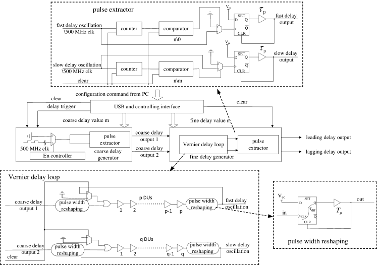
The global architecture of the proposed delay generator is depicted in Fig.2. It mainly contains three parts: the USB and controlling interface, the coarse delay generator and the fine delay generator. The USB and controlling interface is the controlling core of the delay generator. It is in charge of receiving digitally programmable delay values from PC via USB bus, producing the delay trigger and clearing the status after each time of working.
The coarse delay generator is mainly composed of one pulse extractor module whose input ports are fed by the 500 MHz clock signal (denoted as system clock in Fig.1) resulting in the coarse delay resolution of 2 ns which is firstly multiplexed by an En controller module. The En controller module turns to high level after it detects the positive status of the delay trigger at the starting moment T0. According to the functional principle of the pulse extractor, whenever the 500 MHz is selected to pass through the multiplexer, the two counters in the pulse extractor are triggered to run upward. Two delay outputs are generated when the counters equal 0 and respectively. The first generated output is fed to the fast delay loop while the other to the slow delay loop, by this way generating the coarse time interval before the fine delay step functions.
The pulse extractor module is designed to locate and extract the expected pulse from the corresponding oscillation sequence. The pulse to be extracted is predefined by the delay value or . This module contains two counters, two comparators and two D-type flip-flops as shown in Fig.2. The two counters run upward driven by the oscillation sequence from which the expected pulse is to be extracted. The two counters are both driven by the 500 MHz system clock in the coarse delay generator, while respectively by the fast and slow oscillation pulses in the fine delay generator. The counter’s output is connected to its following comparator whose comparison counterpart is one of the customized preset values of 0, and . The two comparators’s preset values are 0 and respectively in the coarse delay generator while both in the fine delay generator. When the counter value equals its comparison counterpart, the comparator outputs a rising edge to activate the D-type flip-flop to generate a delay output. In the special case of the preset value of 0, since it equals the default value of the counter making the comparator to output a constant positive level, the multiplexer is always switched to the 1-th channel. That means the first pulse of the corresponding oscillation signal will be extracted which exactly has zero added delay. A fixed delay buffer is inserted between the Q port and the CLR port of the flip-flop to constrain the pulse width to a proper value.
The fine delay generator contains a Vernier delay loop and another pulse extractor. To facilitate the explanation, the smallest and indivisible basic delay cell along the carry chain is denoted as delay unit (DU) throughout this paper. The Vernier delay loop contains two delay loops constituted of some amount of DUs along the dedicated carry chain in the FPGA (the maximal amount is set as 32 in our example design). Each loop consists of one delay element, one fixed delay buffer, one pulse width reshaping module, one multiplexer and one OR gate. The pulse width reshaping module is designed to constrain and stabilize the positive duration of the oscillation pulse which should be less than . It uses a D flip-flop followed by a delay buffer to fulfill the reshaping function. In our example design, ns and ns.

Obviously construing the two delay loops with slightly different oscillation periods is the most challenging task, and in order to overcome this design difficulty we propose an efficient two-step construction method. It works as follows: in the first step, a delay loop of the structure as shown in Fig.2 is built in a standalone Quartus project and then exported out as the seed loop. In the second step, a new Quartus project is set up and two delay loops are built from the same seed by applying importation operation. The two-step construction method guarantees that the structures of the two delay loops are identical which should ideally lead to an equal oscillation period. However any delay mismatch of the DUs in the two delay loops will break the equation condition and make the oscillation periods different from each other in a random manner. Fortunately according to our building experience, this period difference (or resolution) is always small enough such that it can provide the basis to further finely tune the two delay loops to obtain a desired resolution. The fine-tuning process is applied at the fine-tuning point which is actually the wire connection at the end of each delay loop as shown in Fig.3. The oscillation signals along the two delay loops are brought out from the two fine-tuning points and connected to an external oscilloscope. By observing the relative oscillation periods from the oscilloscope, the resolution of the current delay loops configuration can be deduced. To finely tune the resolution, the following actions are applied: pick up the delay loop that corresponds to the longer oscillation period, disconnect the delay loop at the fine-tuning point, shorten its length by 1 DU, and reconnect it to form the new shorter delay loop. Those actions are iteratively performed until a desired resolution is found. It should be noticed that the regeneration process of the fine-tuning point would change the capacitance condition of the final DU of the delay loops and cause an extra delay. However this effect is not harmful to the fine-tuning process which is an iterative searching process containing many DU number combination possibilities. Some similar works on manually trimming delay path circuits to obtain a desired resolution can be found in JKalisz_TDC1997 ,HaiWang_TDC2013 . In our example design, we realized the mentioned operation using the engineering change orders (ECO) tool provided by the Quartus II software. Our design experience verifies that a wide resolution range of (10 ps, 100 ps) can be constructed.
Small period difference improves the fine delay resolution but raises the risk of larger RMS jitter. This can be illustrated by the following formulas which expresses the proportional relationship between the RMS jitter of the delay interval and the square root of the oscillation time AAAbidi2006 :
| (2) |
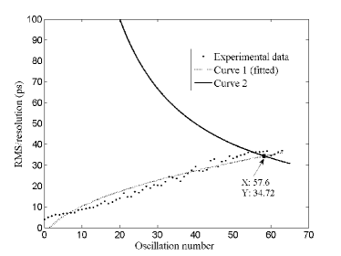
where is a circuit-dependent factor. Here only the fine delay RMS jitter is considered because the coarse delay RMS jitter can be stabilized by the PLL’s feedback loop and is therefore omitted. Equation (2) means the RMS jitter is inversely proportional to square root of the fine resolution which restricts its smallest choice. We experimentally tested the RMS jitter versus the oscillation number and draw the fitted curve in Fig.4 (curve 1). An assistant curve 2 which is modeled by equation representing the resolution versus is also given. These two curves generate a crossing point which has the resolution value of about 35 ps. This point represents the lower resolution bound that guarantees the corresponding RMS jitter not larger than 1 LSB. That means a careful performance tradeoff between the resolution and RMS jitter should be made, and in our example design we choose the resolution of 35 ps as the construction target.
IV Test results
The proposed delay generator was implemented in the EP3SE110F1152I3 Stratix III FPGA from Altera on a self-designed test board. The board also contains a USB interface fulfilled by the CY7C68013 chip from which the digitally programmable delay values are received. The delay generator is configured in a special testing mode for the measurement convenience. In this mode, the delay generator continues to function automatically every 1 s by self-reset. The automation procedure is controlled by the USB interface. The two delay outputs are brought out through two SMA connectors and prolonged by two coaxial cables of the same length to the external 740Zi Lecroy digital oscilloscope with 4 GHz signal bandwidth and 40 GS/s real time sample rate. The oscilloscope directly provides a delay difference measurement tool which calculates the statistical parameters such as the mean and the RMS jitter. More than 5000 hits are accumulated to calculate the statistical results for every testing point.
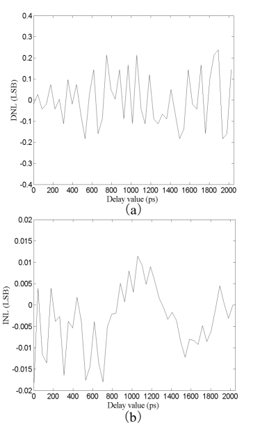
Fig.5 depicts the DNL and INL results which cover the coarse clock period of 2000 ps under the nominal supply voltage of 1100 mV and environmental temperature of 20 ∘C. The maximal fine delay number in the figure is 52 and corresponds to the generated fine delay of about 2010 ps, so the resolution is 2010/52=38.6 ps. The DNL \ INL is in the range of (-0.18 LSB, 0.24 LSB) \ (-0.02 LSB, 0.01 LSB) according to Fig.5. The RMS jitter is tested and depicted in Fig.4 which is used to decide the lower bound of the resolution. The biggest tested RMS jitter for our delay generator is 33.6 ps when equals the maximal value of 52 for the fine dynamic working range. Larger delay value will cause to recirculate from 0 which is constrained never to exceed 52 by means of increasing the coarse delay number accordingly.
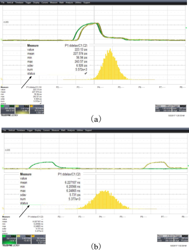
The coarse delay generator uses the clock signal compensated by the PLL which gives little contribution to the overall RMS jitter. Fig.6 shows the waveform and histogram captured by the Lecroy digital oscilloscope when the programmed delay numbers are set to =(0, 6) \ (3, 6) corresponding to the expected delay values of ps \ ps. The tested delay intervals are 228 ps \ 6227 ps and the tested RMS jitters are 6.9 ps \ 5.7 ps. It shows they obtain nearly the same RMS jitter and manifests the fact that is the decisive parameter contributing to the RMS. According to the working principle, the proposed delay generator has a maximal dead time of
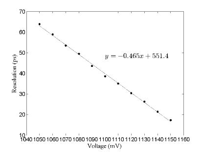
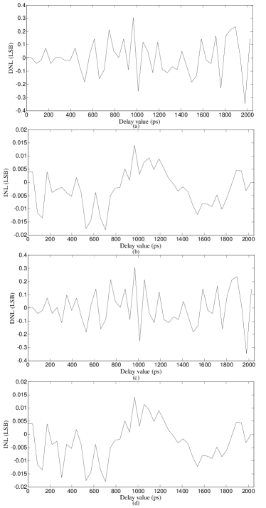
Finally the delay stability against environmental changes such as voltage and temperature is evaluated. For voltage stability consideration, the core voltage of the FPGA chip is scanned from 1050 mV to 1150 mV with a 10 mV interval. The obtained resolution versus voltage is depicted and fitted using a linear function in Fig.7. The fitted voltage drifting coefficient is -0.465 ps/mV according to Fig.7. To visualize the influence of the voltage drift to the DNL and INL performance, we depict the corresponding DNLs and INLs under the voltage conditions of 1050 mV and 1150 mV respectively in Fig.8. It can be seen that voltage drift has very little influence to the DNLs and INLs of which the DNLs lie in the range of (-0.4 LSB, 0.4 LSB) and the INLs in the range of (-0.02 LSB, 0.02 LSB).
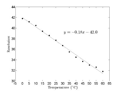
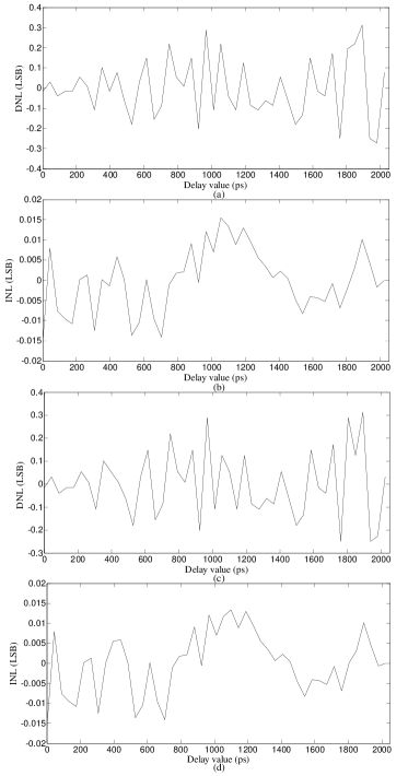
For temperature stability consideration, the entire test board implementing the delay generator is placed in a high-low temperature test chamber by using which a temperature dynamic range from 0 ∘C to 60 ∘C with a 5 ∘C interval is covered. The obtained resolution versus temperature is depicted and fitted using a linear function in Fig.9. The fitted temperature drifting coefficient is -0.18 ps/∘C according to Fig.9. Although the temperature coefficient for a single delay line should be positive as in RGiordano2015 , a negative coefficient is still possible for the Vernier delay line since the temperature change may have much larger influence to the fast delay line compared with the slow delay line. Finally the corresponding DNLs and INLs under the temperature conditions of 0 ∘C and 60 ∘C respectively are depicted in Fig.8. Similarly we conclude that temperature drift has very little influence to the DNLs and INLs of which the DNLs lie in the range of (-0.4 LSB, 0.4 LSB) and the INLs in the range of (-0.02 LSB, 0.02 LSB).
The proposed delay generator is rather resource cost efficient. The compilation report shows the used LUT occupation percentage is 668/85200 (0.7%) and the used register occupation percentage is 146/85200 (0.2%). All required resources are ordinary and widely exist in the FPGA fabric, and this characterization improves its usage convenience and releases the constructing demands.
V Conclusions
We present an delay generator architecture working in the Vernier type based on the dedicated carry chains in the FPGA. The delay generator was implemented in the EP3SE110F1152I3 Stratix III device from Altera on a self-designed test board. Test result shows the obtained resolution is 38.6 ps, and the DNL \ INL is in the range of (-0.18 LSB, 0.24 LSB) \ (-0.02 LSB, 0.01 LSB) under the nominal supply voltage of 1100 mV and environmental temperature of 20 ∘C. The delay generator is rather resource cost efficient which uses only 668 LUTs and 146 registers in total. We believe the proposed delay generator can present powerful usefulness in many physical instruments due to its high-resolution and structural simplicity.
Acknowledgements.
This work was supported by the Fundamental Research Funds for the Central Universities under Grants 30916014112-019 and 30916011349.References
- (1) Y. Liu, H. Li, Y. Wang, T. Xing, H. Baghaei, J. Uribe, R. Farrell, and W.-H. Wong, “A programmable high-resolution ultra-fast delay generator,” IEEE Transactions on Nuclear Science, vol. 50, no. 5, pp. 1487–1490, Oct 2003.
- (2) J. P. Martin and K. Ragan, “A programmable nanosecond digital delay and trigger system,” in Nuclear Science Symposium Conference Record, 2000 IEEE, vol. 2, 2000, pp. 12/141–12/144 vol.2.
- (3) R. Ginosar, “Metastability and synchronizers: A tutorial,” IEEE Design Test of Computers, vol. 28, no. 5, pp. 23–35, Sept 2011.
- (4) H. U. Jang, J. Blieck, G. Veshapidze, M. L. Trachy, and B. D. DePaola, “An auto-incrementing nanosecond delay circuit,” Review of Scientific Instruments, vol. 78, no. 9, p. 094702, 2007.
- (5) J. Kalisz, A. Poniecki, and K. Różyc, “A simple, precise, and low jitter delay/gate generator,” Review of Scientific Instruments, vol. 74, no. 7, pp. 3507–3509, 2003.
- (6) Y. Song, H. Liang, L. Zhou, J. Du, J. Ma, and Z. Yue, “Large dynamic range high resolution digital delay generator based on FPGA,” in Electronics, Communications and Control (ICECC), 2011 International Conference on, Sept 2011, pp. 2116–2118.
- (7) R. Giordano, F. Ameli, P. Bifulco, V. Bocci, S. Cadeddu, V. Izzo, A. Lai, S. Mastroianni, and A. Aloisio, “High-resolution synthesizable digitally-controlled delay lines,” IEEE Transactions on Nuclear Science, vol. 62, no. 6, pp. 3163–3171, Dec 2015.
- (8) K. Cui, Z. Ren, X. Li, Z. Liu, and R. Zhu, “A high-linearity, ring-oscillator-based, Vernier time-to-digital converter utilizing carry chains in FPGAs,” IEEE Transactions on Nuclear Science, vol. 64, no. 1, pp. 697–704, Jan 2017.
- (9) J. Y. Won and J. S. Lee, “Time-to-digital converter using a tuned-delay line evaluated in 28-, 40-, and 45-nm FPGAs,” IEEE Transactions on Instrumentation and Measurement, vol. 65, no. 7, pp. 1678–1689, July 2016.
- (10) Y. Wang and C. Liu, “A 3.9 ps time-interval RMS precision time-to-digital converter using a dual-sampling method in an UltraScale FPGA,” IEEE Transactions on Nuclear Science, vol. 63, no. 5, pp. 2617–2621, Oct 2016.
- (11) J. Yu, F. F. Dai, and R. C. Jaeger, “A 12-bit Vernier ring time-to-digital converter in 0.13 um CMOS technology,” IEEE Journal of Solid-State Circuits, vol. 45, no. 4, pp. 830–842, April 2010.
- (12) J. Kalisz, R. Szplet, J. Pasierbinski, and A. Poniecki, “Field-programmable-gate-array-based time-to-digital converter with 200-ps resolution,” IEEE Transactions on Instrumentation and Measurement, vol. 46, no. 1, pp. 51–55, Feb 1997.
- (13) H. Wang, M. Zhang, and Q. Yao, “A new realization of time-to-digital converters based on FPGA internal routing resources,” IEEE Transactions on Ultrasonics, Ferroelectrics, and Frequency Control, vol. 60, no. 9, pp. 1787–1795, Sep 2013.
- (14) A. A. Abidi, “Phase noise and jitter in CMOS ring oscillators,” IEEE Journal of Solid-State Circuits, vol. 41, no. 8, pp. 1803–1816, Aug 2006.