Mach-Zehnder interferometry using spin- and valley-polarized quantum Hall edge states in graphene
Confined to a two-dimensional plane, electrons in a strong magnetic field travel along the edge in one-dimensional quantum Hall channels that are protected against backscattering. These channels can be used as solid-state analogues of monochromatic beams of light, providing a unique platform for studying electron interference. Electron interferometry is regarded as one of the most promising routes for studying fractional and non-Abelian statistics and quantum entanglement via two-particle interference. However, creating an edge-channel interferometer in which electron-electron interactions play an important role requires a clean system and long phase coherence lengths. Here we realize electronic Mach-Zehnder interferometers with record visibilities of up to 98 using spin- and valley-polarized edge channels that co-propagate along a PN junction in graphene. We find that inter-channel scattering between same-spin edge channels along the physical graphene edge can be used to form beamsplitters, while the absence of inter-channel scattering along gate-defined interfaces can be used to form isolated interferometer arms. Surprisingly, our interferometer is robust to dephasing effects at energies an order of magnitude larger than observed in pioneering experiments on GaAs/AlGaAs quantum wells. Our results shed light on the nature of edge-channel equilibration and open up new possibilities for studying exotic electron statistics and quantum phenomena.
I Introduction
Electron interference plays a central role in mesoscopic physics Datta1995 ; Chamon1997 ; Ji2003 and is regarded as one of the most promising routes for studying fractional and non-Abelian statistics Law2006 ; Feldman2006 and quantum entanglement via two-particle interference Samuelsson2004 ; Yurke1992 . Quantum Hall edges form excellent building blocks for electron interferometers as they are single-mode channels that are protected from inter-channel scattering by their quantum degrees of freedom such as spin Datta1995 ; Amet2014 . Furthermore, they can be positioned via electrostatic gating and coupled at target locations that act as beamsplitters Chamon1997 ; Ji2003 . Graphene may provide an advantage compared to conventional GaAs edge-channel interferometers Neder2006 ; Neder2007 ; Roulleau2007 ; Bieri2009 as the absence of a band gap allows the creation of hole- and electron-like edge channels that naturally meet, co-propagate, and separate at gate-defined PN interfaces Abanin2007 ; Williams2007 . Moreover, the additional valley degree of freedom and the associated unique nature of graphene quantum Hall states CastroNeto2009 ; Young2012 open up new opportunities for addressing long-sought goals of electron interferometry such as the observation of non-Abelian statistics Zibrov2017 . In addition, the valley isospin provides new possibilities for controlling inter-channel scattering Tworzydlo2007 , a requirement for creating edge-channel interferometers. However, even though graphene PN junctions in the quantum Hall regime have been studied extensively Amet2014 ; Abanin2007 ; Williams2007 ; Ozyilmaz2007 ; Velasco2009 ; Matsuo2015 ; Machida2015 ; Tovari2016 , creating an edge-channel interferometer using spin- and valley-polarized edge channels has remained an outstanding challenge.
In the paradigmatic electronic interferometer — the Mach-Zehnder interferometer (MZI) Ji2003 — a beam of electrons is split into two paths by a beam splitter and recombined at a second beam splitter. Here, we engineer MZIs consisting of same-spin, opposite-valley quantum Hall edge channels that co-propagate along a PN junction in graphene. Using magnetic and trans-junction electric fields, we can tune into a regime in which either one or both pairs of the same-spin edge channels belonging to the zeroth Landau level (zLL) form MZIs that coherently mediate the cross-junction transport (Fig. 1A). We find that these channels can be well isolated from those belonging to other Landau levels (LLs), enabling us to study a target interferometer over a large range of electric fields and tune into regimes with visibilities as high as 98. By studying PN interfaces of different lengths, we show that the interferometer beamsplitters are located where the PN interface meets the physical graphene edges, which we attribute to strong inter-valley scattering at the physical graphene edge and the absence of inter-valley scattering along the gate-defined edge. We independently verify this conclusion using a device in which we can tune the number of edge channels co-propagating along either a physical or gate-defined edge.
II Results
II.1 Constructing a Mach-Zehnder interferometer in a graphene PN junction
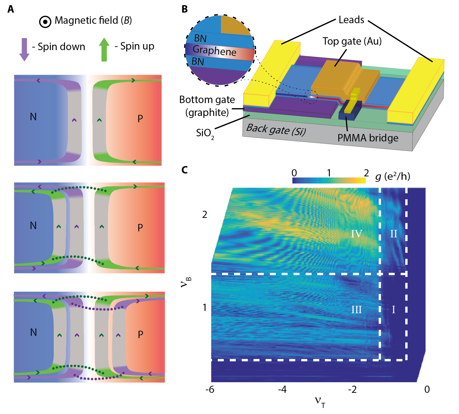
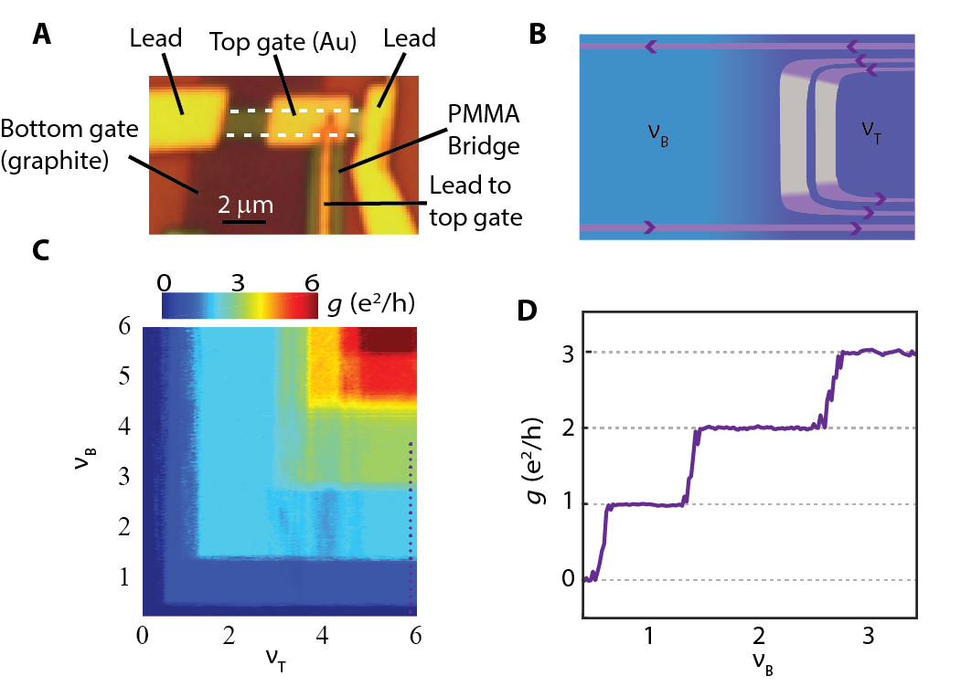
To construct a MZI of spin- and valley-polarized edge channels, we use a hexagonal boron nitride (hBN) encapsulated monolayer of graphene (Fig. 1B and Methods). We tune into the quantum Hall regime using a perpendicular magnetic field B, and define two regions of different charge densities and using a bottom gate that affects both and and a top gate that affects only (Fig. 1B). The number of edge channels in these regions is given by the filling factors , where is the electron charge and is Planck’s constant. The observation of integer quantum Hall steps in a measurement of the two-terminal conductance at B = 4 T in the regime where and confirms that the spin- and valley-degeneracy is lifted (Supplementary Fig. 1).
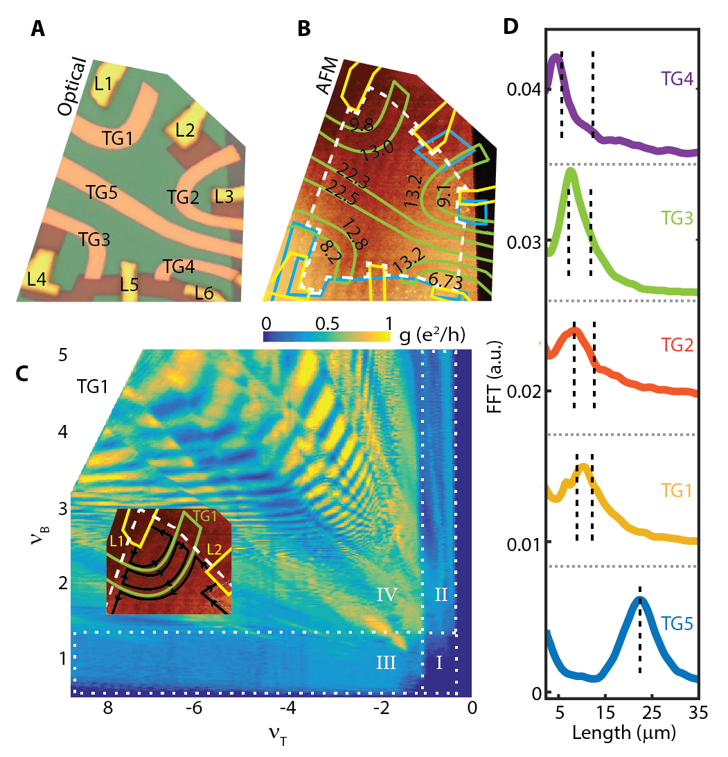
Next, we create a PN junction by tuning into the regime where and and study which edge channels mediate charge transport across the junction. When we measure the conductance as a function of and at B = 4 T (Methods), we observe four regions with distinct ranges of conductance values, as well as the first indications of conductance oscillations (Fig. 1C). In region I, the conductance of the junction is near zero, which we attribute to the situation depicted in the top panel of Fig. 1A (where and ). Here, one N-type spin-down and one P-type spin-up edge channel co-propagate along the junction. As these channels have opposite spin, inter-channel scattering is suppressed Amet2014 . When we cross from region I into region II, we begin to observe transport across the junction. We attribute this to an additional spin-up edge channel having entered on the N-side (so that and ) and that electrons in this channel can scatter into the spin-up channel on the P-side (see middle panel in Fig. 1A). The observed conductance ranges approximately between 0 and , consistent with one pair of edge channels mediating transport across the junction. Similarly, in region III we obtain the situation in which and , and we attribute the observed conductance to scattering between the two spin-down edge channels. Strikingly, in region III the conductance does not change notably as we keep adding edge channels on the P-side (going to and ). We conclude that these additional channels do not contribute to the trans-junction conductance, presumably because they belong to a higher LL which makes them spatially too distant from the PN interface. Crossing into region IV ( and ), we observe that the average conductance increases and ranges between 0 and . We attribute this to two pairs of same-spin edge channels mediating transport across the junction. Again, we see no sign of edge channels belonging to higher LLs entering the system and contributing to the trans-junction conductance. We conclude that the edge channels belonging to the zLL mediate the trans-junction conductance, well isolated from edge channels belonging to higher LLs.
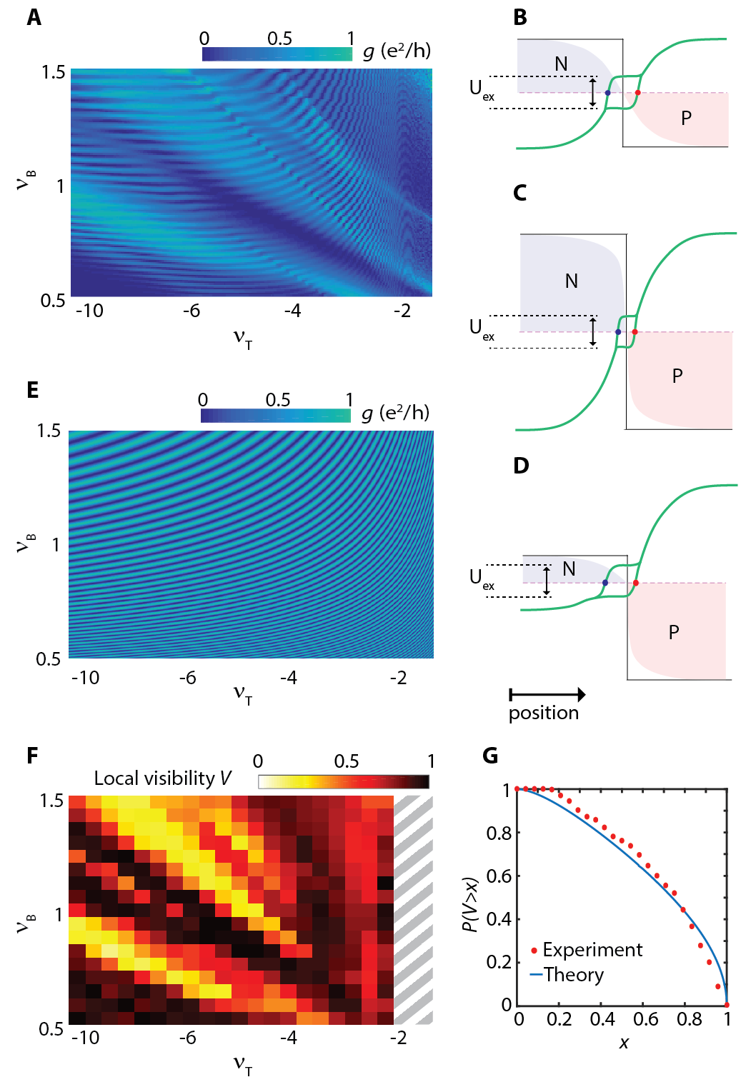
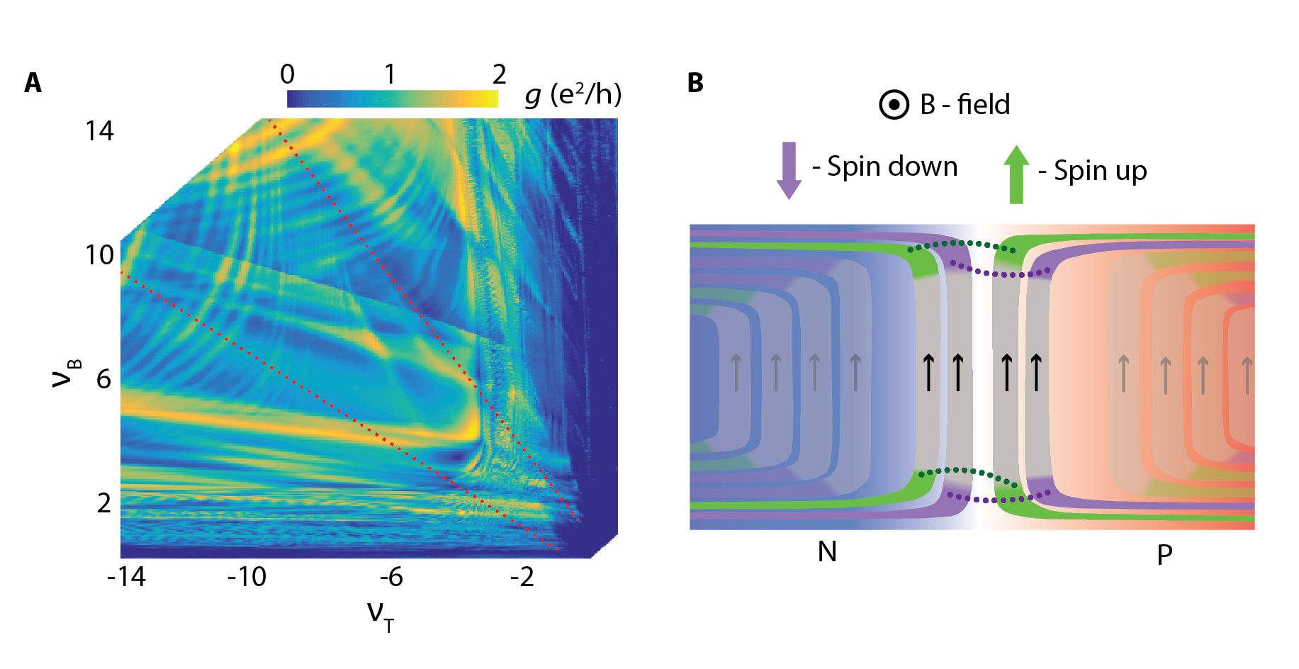
The relative isolation of the edge channels that belong to the zLL allows us to study a target pair of edge channels over a large range of filling factors. As we increase the magnetic field to B = 9 T and concentrate on region III, in which and , we observe a striking pattern of conductance oscillations (Fig. 2A) whose key features such as shape and periodicity depend on both and . These oscillations cannot be explained by semi-classical snake states or similar low-field phenomena Williams2011 ; Rickhaus2015 ; Taychatanapat2015 ; Overweg2016 since in our device electron transport is mediated by quantum Hall edge channels. Instead, as we will further argue below, the well-defined periodicity of these oscillations indicates that scattering between the two edge channels that mediate the cross-junction transport occurs at only two points along the junction. These points form the beamsplitters that define our MZI. Its conductance, in units of , is given by
| (1) |
where () is the transmission (reflection) amplitude of the -th beamsplitter, with . The phase arises from the Aharonov-Bohm effect, where is the flux quantum, A the effective area enclosed by the two edge channels, and an (unknown) phase associated with the beamsplitters.
Since the measurement in Fig. 2A is performed at a fixed magnetic field, we attribute the conductance oscillations to a changing distance between the two edge channels and a resulting changing flux through the interferometer. We can analyze the charge-density-dependent locations of these channels by determining where the two corresponding exchange-split Landau sublevels cross the Fermi energy, using a simple model for the spatial dependence of the sublevel energy (Fig. 2B-D and Supplementary Note 1). This model indicates that as the charge densities increase (from Fig. 2B to Fig. 2C), the edge-channel separation decreases. Furthermore, when the charge density is small (large) on a particular side of the junction, the edge-channel separation is relatively sensitive (insensitive) to the charge density on that side of the junction (Fig. 2D). Figure 2E shows that this model reproduces the key features of the data in Fig. 2A. Further data in the and regime, in which two MZIs act simultaneously (as depicted in the bottom panel of Fig. 1A), are shown in Supplementary Fig. 2.
II.2 Beamsplitter characteristics
The visibility of the oscillations in a MZI depends on the phase coherence and the transmission characteristics of the beamsplitters. We analyze the range of visibilities observed in the measurement shown in Fig. 2A by dividing the measurement range into a grid and calculating the local visibility , with and the maximum and minimum conductance within each block (Fig. 2F). In Fig. 2G we plot the resulting experimental cumulative probability distribution function that indicates the probability of finding a visibility greater than . This distribution corresponds well to a theoretical prediction that is based on the assumption that the incoming and outgoing channels of each of the two beamsplitters of the MZI are connected by random matrices in valley space (Supplementary Note 2). Remarkably, in several regions of the conductance map (Fig. 2A) we find visibilities as high as 98, indicating near-perfect phase coherence along the PN interface. Additionally, in some regions the conductance oscillates nearly between 0 and , indicating nearly 50/50 beam splitters.
II.3 Dependence of the Mach-Zehnder interference on magnetic field and DC voltage bias
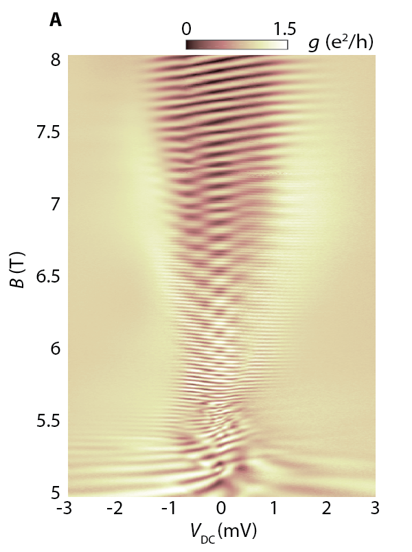
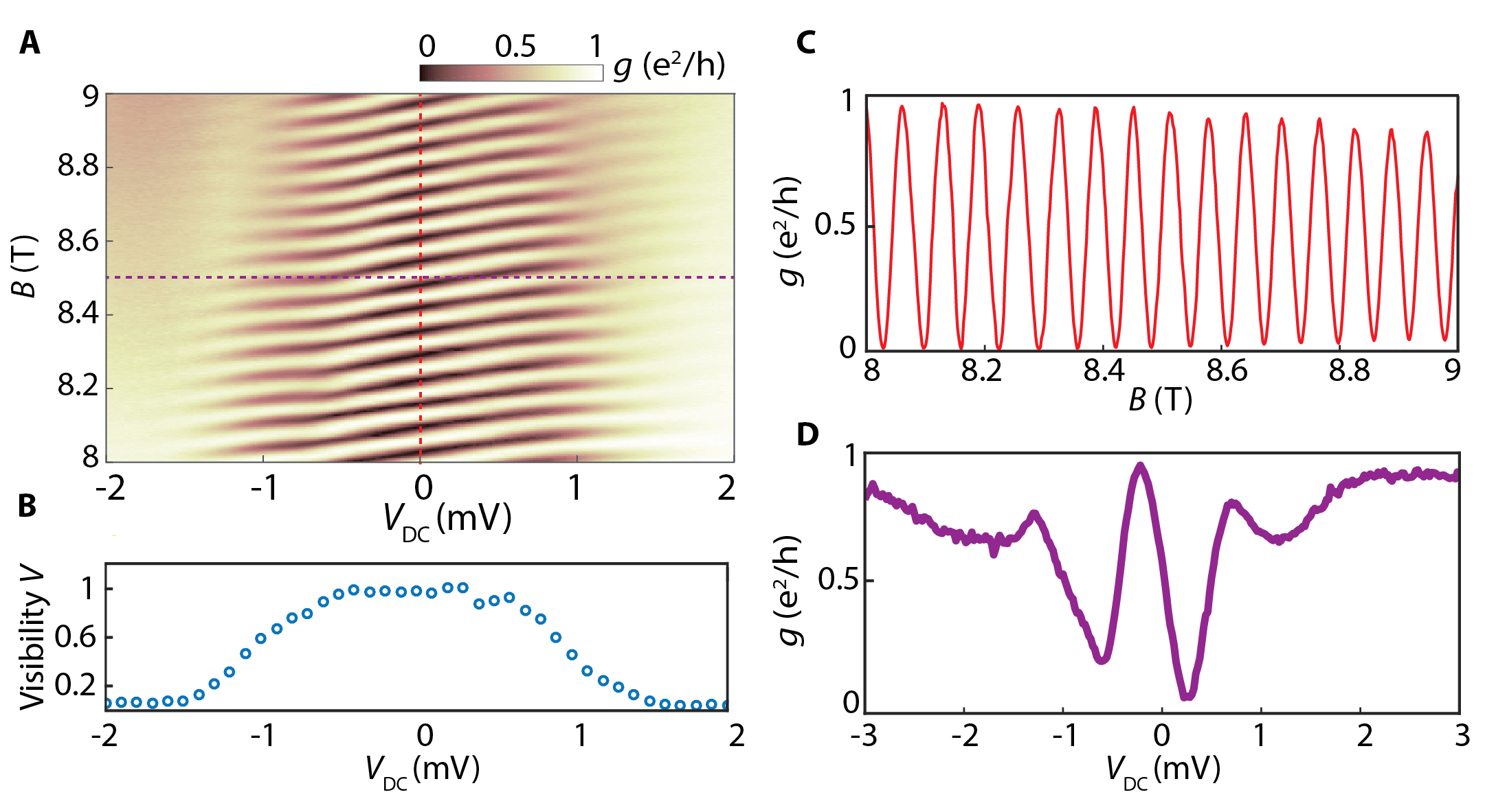
Next, we tune to a region of high visibility and study the conductance as a function of B and a DC voltage bias (Fig. 3A). We observe that the visibility stays near-unity for mV (Fig. 3B), and decreases at larger , which may be due to thermal averaging or electron-electron interactions Ji2003 ; Bieri2009 . For the 8 to 9 T field range of Fig. 3C, measurements at show a constant oscillation period , which is consistent with an assumption that the area enclosed by the interferometer is constant and given by . Subject to this assumption, we determine an edge-channel separation of 52 nm. Oscillations with are also observed (Fig. 3D) indicating a bias-dependent edge-channel separation, which may be a result of a bias-induced electrostatic gating effect Bieri2009 . We note that at larger filling factors we see multiple frequencies, changing frequency with field, and lobe structures, which have previously been attributed to Coulomb interactions in GaAs devices Neder2006 ; Roulleau2007 ; Bieri2009 (Supplementary Fig. 3). We leave the analysis of these effects to a future study.
II.4 Varying the length of the PN interface
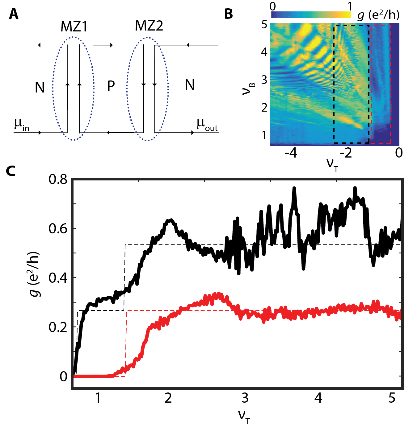
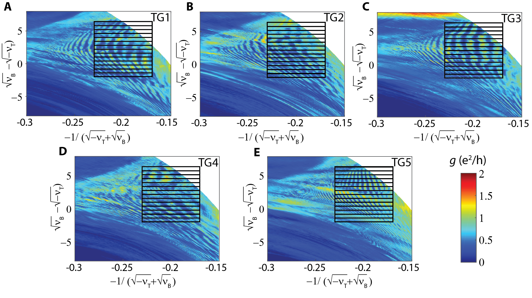
To confirm that the beamsplitters are located where the PN interface meets the physical graphene edges, we measure the MZI oscillation frequency as a function of the interface length. We use device 2 (Fig. 4A-B), which has five top gates (TG1 to TG5) of varying lengths that we can address individually in two-terminal conductance measurements by using the appropriate leads. Using top and bottom gates to control the filling factors in the top-gated and non-top-gated regions, and respectively, we can tune into a regime where and to create an NPN configuration with two PN junctions in series (Supplementary Fig. 4). When we measure the two-terminal conductance at B = 8 T as a function of and (Fig. 4C and Supplementary Fig. 4), we recognize the regions corresponding to zero, one, and two pairs of same-spin edge channels mediating transport across the PN junctions, as discussed above for the measurement in Fig. 1C and further analyzed in Supplementary Note 3. In addition, we observe clear conductance oscillations, of which we expect the frequencies to reflect the gate lengths. To analyze these frequencies, we focus on the limit in which the edge-channel separation and the associated Aharanov-Bohm flux are expected to vary as ) (Supplementary Note 4). We plot the conductance data against ) and use a Fourier transform to determine the frequency spectrum (Supplementary Fig. 5). Normalizing the frequency axis to the average length of TG5, we find peaks at locations that correspond reasonably well to those expected based on the lengths of the different gates (Fig. 4D). We conclude that the beamsplitters are located where the PN interfaces meet the physical graphene edge. Remarkably, it follows that each oscillation corresponds to a minute change in the edge-channel separation: for example, for the L=1.2 m gate length of device 1, this change equals Å.
II.5 Edge-channel equilibration along gate-defined and physical edges
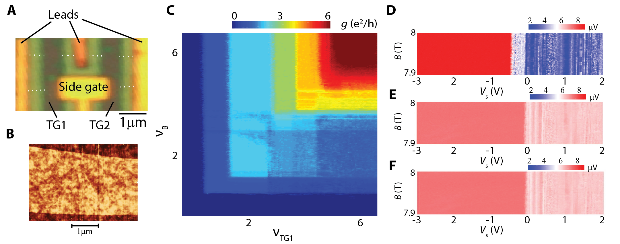
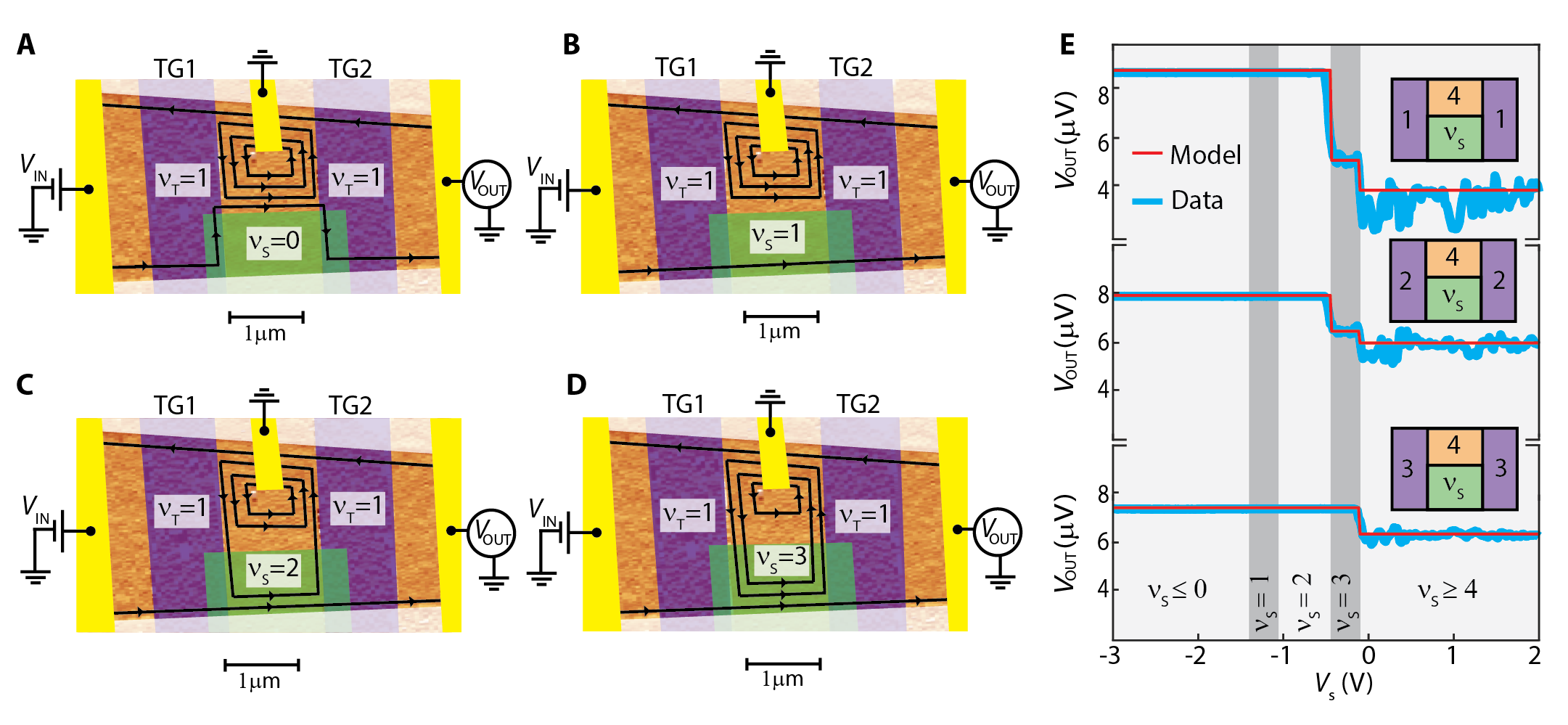
Finally, we demonstrate the absence of inter-channel scattering along a gate-defined edge and the full equilibration of same-spin edge channels running along a physical edge. We use device 3 (Fig. 5A-D), which has two top gates that determine the number of edge channels running from the left to the right lead, and a top gate (referred to as the side gate) that determines which fraction of the edge channels in the central region travel along the lower physical edge instead of along the side-gate-defined edge. We first confirm the presence of robust broken-symmetry quantum Hall states (Supplementary Fig. 6C). We then apply a bias between the left and top lead, and measure the potential at the right lead () as a function of the side-gate filling factor (Fig. 5E). Edge-channel equilibration in the central region should reduce the chemical potential at the right lead below that of the input lead. The precise match between data and model (described in Supplementary Note 5) in Fig. 5E clearly demonstrates that edge channels do not equilibrate along the side-gate-defined edge, while they do equilibrate along the physical edge provided they have the same spin Amet2014 . We note that we observe no MZI oscillations as we sweep the magnetic field between 8.9 and 9 T (Supplementary Fig. 6D-F), presumably because there are no locations acting as beamsplitters as the edge channels do not meet at a physical edge before and after co-propagating along a gate-defined edge.
III Discussion
The experiments presented here demonstrate a robust method of engineering a high-visibility MZI in a graphene QH system. This opens up the possibility of a variety of interferometry experiments and grants us the diagnostic capabilities of measuring sub-nanometer shifts in edge-channel separation. In our experiments we observe transport across the insulating state, which is expected to be in a canted antiferromagnetic (CAF) phase in bulk graphene Kharitonov2012 ; Young2014 . The fact that we find that spin polarization is well preserved in our samples suggests that the CAF phase may be suppressed in a narrow PN junction in favor of a state where spins are fully polarized along the direction of the magnetic field.
IV Methods
IV.1 Sample Fabrication
All devices were fabricated on doped Si chips with a 285 nm layer of that acted as a dielectric for the Si back gate. Graphene was mechanically exfoliated from bulk graphite obtained from NGS Naturgraphit GmbH using 1009R tape from Ultron Systems and subsequently encapsulated in hexagonal boron nitride (hBN) using a dry transfer process Wang2013 . For device 1, we placed the resulting stack on a graphite bottom gate. Before the first metal deposition step, we annealed the devices in vacuum at 500∘C to improve device quality. We then created top gates using electron-beam lithography and thermal evaporation of Cr/Au. To fabricate edge-contacts to the graphene in device 1 without shorting to the graphite bottom gate, we selectively etched the stack down such that the bottom hBN flake remained and protected the graphite while simultaneously exposing the graphene flake. To fabricate edge-contacts to the graphene in devices 2 and 3, we etched through the entire hBN/graphene stack. We then created edge contacts by thermally evaporating Cr/Au while rotating the sample using a tilted rotation stage. Finally, we etched the devices into the desired geometry by reactive ion etching in using a PMMA/HSQ bilayer of resist (patterned by electron-beam lithography) as the etch mask.
IV.2 Measurement
Our measurements were performed in a Leiden dry dilution refrigerator with a base temperature of 20 mK. Measurements of differential conductance were performed using a lock-in amplifier with an AC excitation voltage of 10 V at 17.77 Hz. All measurements of differential conductance were corrected for contact/line resistances, which were independently determined by lining up the robust quantum Hall conductance plateau with . We estimated all filling factors based on a parallel-plate capacitor model with a correction to account for quantum capacitance (Supplementary Note 6).
References
- (1) Datta, S. Electronic Transport in Mesoscopic Systems (Cambridge Univ. Press, 1995).
- (2) Chamon, C. C., Freed, D. E., Kivelson, S. A., Sondhi, S. L. & Wen, X. G. Two point-contact interferometer for quantum Hall systems. Phys. Rev. B 55, 2331–2343 (1997).
- (3) Ji, Y., Chung, Y., Sprinzak, D., Heiblum, M. & Mahalu, D. An electronic Mach-Zehnder interferometer. Nature 422, 415–418 (2003).
- (4) Law, K. T., Feldman, D. E. & Gefen, Y. Electronic Mach-Zehnder interferometer as a tool to probe fractional statistics. Phys. Rev. B 74, 045319 (2006).
- (5) Feldman, D. E. & Kitaev, A. Detecting non-abelian statistics with an electronic Mach-Zehnder interferometer. Phys. Rev. Lett. 97, 186803 (2006).
- (6) Samuelsson, P., Sukhorukov, E. V. & Büttiker, M. Two-particle Aharonov-Bohm effect and entanglement in the electronic Hanbury Brown-Twiss setup. Phys. Rev. Lett. 92, 026805 (2004).
- (7) Yurke, B. & Stoler, D. Bell’s-inequality experiments using independent-particle sources. Phys. Rev. A 46, 2229–2234 (1992).
- (8) Amet, F., Williams, J. R., Watanabe, K., Taniguchi, T. & Goldhaber-Gordon, D. Selective equilibration of spin-polarized quantum Hall edge states in graphene. Phys. Rev. Lett. 112, 196601 (2014).
- (9) Neder, I., Heiblum, M., Levinson, Y., Mahalu, D. & Umansky, V. Unexpected behavior in a two-path electron interferometer. Physical Review Letters 96, 1–4 (2006).
- (10) Neder, I. et al. Interference between two indistinguishable electrons from independent sources. Nature 448, 333–337 (2007).
- (11) Roulleau, P. et al. Finite bias visibility of the electronic Mach-Zehnder interferometer. Physical Review B 76, 161309 (2007).
- (12) Bieri, E. et al. Finite-bias visibility dependence in an electronic Mach-Zehnder interferometer. Phys. Rev. B 79, 245324 (2009).
- (13) Abanin, D. A. & Levitov, L. S. Quantized transport in graphene p-n junctions in a magnetic field. Science 317, 641–643 (2007).
- (14) Williams, J. R., Dicarlo, L. & Marcus, C. M. Quantum Hall effect in a gate-controlled p-n junction of graphene. Science 317, 638–640 (2007).
- (15) Castro Neto, A. H., Guinea, F., Peres, N. M. R., Novoselov, K. S. & Geim, A. K. The electronic properties of graphene. Rev. Mod. Phys. 81, 109–162 (2009).
- (16) Young, A. F. et al. Spin and valley quantum Hall ferromagnetism in graphene. Nature Physics 8, 550–556 (2012).
- (17) Zibrov, A. et al. Robust nonabelian ground states and continuous quantum phase transitions in a half filled bilayer graphene Landau level. Preprint at https://arxiv.org/abs/1611.07113 (2016).
- (18) Tworzydło, J., Snyman, I., Akhmerov, A. R. & Beenakker, C. W. J. Valley-isospin dependence of the quantum Hall effect in a graphene junction. Phys. Rev. B 76, 035411 (2007).
- (19) Özyilmaz, B. et al. Electronic transport and quantum Hall effect in bipolar graphene p-n-p Junctions. Phys. Rev. Lett. 99, 166804 (2007).
- (20) Velasco, J., Liu, G., Bao, W. & Ning Lau, C. Electrical transport in high-quality graphene pnp junctions. New Journal of Physics 11, 095008 (2009).
- (21) Matsuo, S. et al. Edge mixing dynamics in graphene p-n junctions in the quantum Hall regime. Nature Communications 6, 8066 (2015).
- (22) Machida, T. et al. Edge-channel transport of Dirac fermions in graphene quantum Hall junctions. Journal of the Physical Society of Japan 84, 1–9 (2015).
- (23) Tovari, E. et al. Gate-controlled conductance enhancement from quantum Hall channels along graphene p-n junctions. Nanoscale 8, 19910–19916 (2016).
- (24) Williams, J. R. & Marcus, C. M. Snake states along graphene junctions. Phys. Rev. Lett. 107, 046602 (2011).
- (25) Rickhaus, P. et al. Snake trajectories in ultraclean graphene p–n junctions. Nature Communications 6, 6470 (2015).
- (26) Taychatanapat, T. et al. Conductance oscillations induced by ballistic snake states in a graphene heterojunction. Nature Communications 6, 6093 (2015).
- (27) Overweg, H. et al. Oscillating magnetoresistance in graphene p-n junctions at intermediate magnetic fields. Preprint at https://arxiv.org/abs/1612.07624 (2016).
- (28) Kharitonov, M. Phase diagram for the quantum hall state in monolayer graphene. Phys. Rev. B 85, 155439 (2012).
- (29) Young, A. F. et al. Tunable symmetry breaking and helical edge transport in a graphene quantum spin Hall state. Nature 505, 528–32 (2014).
- (30) Wang, L. et al. One-dimensional electrical contact to a two-dimensional material. Science 342, 614–7 (2013).
- (31) Zhang, Y., Tan, Y.-W., Stormer, H. L. & Kim, P. Experimental observation of the quantum Hall effect and Berry’s phase in graphene. Nature 438, 201–204 (2005).
- (32) McClure, D. T. et al. Edge-state velocity and coherence in a quantum Hall Fabry-Pérot interferometer. Phys. Rev. Lett. 103, 206806 (2009).
V Acknowledgements
V.1 General
We acknowledge helpful discussions and feedback from A. Kou, B.E. Feldman, D. Nandi, K. Shain, P. Kim, A. Stern, M. Heiblum, C. Schonenberger, K. Wang, S.L. Tomarken and S.P. Harvey. We also thank G.H. Lee, J.I.J. Wang, J.Y. Luo and X. Liu for help with fabrication.
V.2 Funding
This work was primarily supported by the US DOE, BES Office, Division of Materials Sciences and Engineering under Award DE-SC0001819 (D.S.W., J.D.S.Y., P.J.H. and A.Y.). D.S.W. acknowledges partial support from the National Science Foundation Graduate Research Fellowship under Grant No. DGE1144152. B.I.H. acknowledges support from the STC Center for Integrated Quantum Materials, NSF grant DMR-1231319. K.W. and T.T. acknowledge support from the Elemental Strategy Initiative conducted by the MEXT, Japan and JSPS KAKENHI Grant Numbers JP26248061, JP15K21722 and JP25106006. This work was performed in part at the Harvard University Center for Nanoscale Systems (CNS), a member of the National Nanotechnology Coordinated Infrastructure Network (NNCI), which is supported by the National Science Foundation under NSF ECCS award no. 1541959.
V.3 Author Contributions
D.S.W., T.S., B.I.H. and A.Y. conceived and designed the experiments. D.S.W. fabricated the devices. D.S.W., T.S., J.D.S.Y. and A.Y. performed the experiments. D.S.W., T.S., J.D.S.Y., P.J.-H., B.I.H. and A.Y. analyzed the data, developed the models, and wrote the paper. K.W. and T.T. provided the hexagonal boron nitride crystals used in the devices.
VI Correspondence
Correspondence and requests for materials should be addressed to D.S.W. (email: diwei@fas.harvard.edu).
VII Supplementary Information
VII.1 Supplementary Note 1. Modeling the distance between the edge channels forming a Mach-Zehnder interferometer
In this note we describe the model used for the calculations shown in Fig. 2E of the main text, which shows the conductance of a PN junction as a function of filling factors to the left and right of the PN junction, and , respectively. As discussed in the main text, we attribute the oscillations to a changing flux enclosed by the two edge channels forming a Mach-Zehnder interferometer. At fixed magnetic field, this change is caused by a change in distance between the edge channels. We analyze the locations of the two interferometer-forming edge channels by determining where the corresponding exchange-split Landau sublevels cross the Fermi energy, using a simple model for the spatial dependence of the sublevel energy described by
| (S1) |
where is the chemical potential to the left (right) of the junction, is the exchange splitting, and is a function that smoothly changes from -1 to 1 across the PN junction over a distance that is similar to the distance of the graphene to the gates. For simplicity, from now on we neglect the spatial dependence of . To link the chemical potentials to filling factors, we note that in general , which increases stepwise as Landau levels are filled. For simplicity, we make the approximation , where and is the Fermi velocity Zhang2005 . Defining , and limiting ourselves to the case of and relevant in our PN measurements, we get
| (S2) |
where we have defined . The location of an edge channel is then obtained by solving , so that the distance between two edge channels is given by
| (S3) |
For we use a logistic function of width :
| (S4) |
This has the inverse
| (S5) |
Combining Eqs. S3 and S5, we find the distance between the two edge channels
| (S6) |
To calculate the plot of Fig. 2E, we now assume a MZ interferometer with 50/50 beam splitters and calculate the conductance using
| (S7) |
In Fig. 2E, we used B = 9 T, L = 1.2 m, , W = 52 nm and, to qualitatively resemble the data, =0.4.
VII.2 Supplementary Note 2. Random scattering model for a MZ interferometer at a graphene PN junction
In this note we provide a background discussion of the electronic wavefunctions corresponding to the edge channels that form an interferometer along the PN junction. We then analyze the probability to find a particular visibility of the Mach-Zehnder conductance oscillations for an interferometer that has beamsplitters described by random transmission/reflection matrices. The resulting cumulative probability distribution function for the visibility is shown as the theoretical curve in Fig. 2G of the main text.
Straight junction of infinite length
Let us first consider the case of an infinite, translationally-invariant PN junction aligned with the y-axis. The overall problem can be formulated in terms of a solution to the time-independent single-particle Schrödinger equation at an energy E equal to the Fermi energy. We may write this solution in the form , where is a valley index, and we consider only one spin state. We work in a gauge where the vector potential is parallel to the junction. Then, if there are just two edge states at the junction, we may write, in the vicinity of the junction
| (S8) |
where , for j = 1,2, are the two eigenvalues of the translation operator, are the corresponding eigenvectors, and are arbitrary constants. It will be convenient to choose the normalizations of so that
| (S9) |
where is the velocity of the edge mode.
In the simplest model that we have in mind, the functions will have the approximate form
| (S10) |
where is the magnetic length, is the center of gravity of the state j, and the spinor is a function of the valley index . The separation may be written as
| (S11) |
where is the gradient of the electrostatic potential and is the exchange splitting, which we assume to be constants in the vicinity of the p-n junction. The separation is related to the momentum difference by
| (S12) |
The exchange splitting in Eq. (2.4) results from a term in the Hartree-Fock Hamiltonian of form:
| (S13) |
where is a three-component unit vector and are the three Pauli matrices, acting on the valley index . In an approximation where one neglects valley-dependent electron-electron interactions, which only occur when two electrons are very close together, there is nothing to pick out one particular orientation of over another. Nevertheless, the exchange splitting may be greater than zero. The choice of at a particular PN junction will then depend on small symmetry breaking terms, which we will not attempt to predict, and it could vary as one moves along the junction. The spinors are the eigenstates of .
The magnitude of the exchange splitting must be determined self-consistently, based on the local difference in the occupation of the two valley states. On the microscopic level, we would expect that the exchange potential is not actually a constant over the range of the width of the PN junction, so the quantity in the above equations should be taken as an average over a region covered by the wave functions .
It is straightforward to generalize the discussion of a translationally invariant junction to a situation where properties of the junction, including its orientation, may vary adiabatically along its length. (“Adiabatically” means that the distance scale for changes along the length of the junction should be large compared to .) We choose a gauge where the vector potential is always oriented parallel to the junction at the position of the junction. We may now write
| (S14) |
| (S15) |
where y is the distance along the edge and is measured in the local perpendicular direction. The fact that the magnitudes are independent of is a consequence of conservation of current and our choice for the normalization of .
Junction connected to sample edges
Now we consider a PN junction of length , connected to the sample boundaries at its two ends as depicted in Fig. 1A. We assume that there is a single chiral edge state at any segment of the boundary, and we assume that the edge states at flow into the junction while the edge states at flow away from the junction. The portions of the wave function incident at may be characterized by complex amplitudes and , such that and are, respectively, the currents incident from the left and from the right. Similarly, we may characterize the outgoing wave function by amplitudes and for electrons moving to the right and left, respectively, away from the end of the junction at .
The amplitudes for the wave function along the PN junction will be related to the amplitudes by a 2 x 2 unitary matrix , whose form will depend on details of the sample in the region where the junction meets the edge. Similarly, we may define a matrix , which relates the outgoing amplitudes to the amplitudes at the end of the PN junction. The outgoing amplitudes will then be related to the incoming amplitudes by a matrix , which we may write as
| (S16) |
where is a diagonal matrix with elements . Suppose that there is incident beam impinging on the junction from the left, so that . Defining the transmission coefficient as the probability for an electron to wind up in the right-moving state after leaving the junction, we see that
| (S17) |
Let be the unit vector on the Bloch sphere that corresponds to the two-component unit vector , and let be the unit vector on the Bloch sphere that corresponds to the two-component unit vector . Let by the matrix that represents a rotation by an angle about the z-axis, where
| (S18) |
Then we have
| (S19) |
If we describe the vectors and by their polar coordinates, , and define then we obtain
| (S20) |
| (S21) |
where we recognize Eq. 1 of the main text with and . If the length is large, the phase will change by a large amount when we vary the magnetic field by an amount that is still too small to affect the other parameters in the above equation. Thus will oscillate between maximum and minimum values given by
| (S22) |
If we define the visibility by
| (S23) |
then we find
| (S24) |
Random scattering model
Since the matrices and depend on details that we do not know how to calculate, we will consider a model in which the matrices are random matrices in the group . In this case, the unit vectors and will be randomly distributed on the Bloch sphere. We wish to calculate the probability that the visibility is greater than 1 - . It is useful to change variables to
| (S25) |
The probability is then given by:
| (S26) |
where is the area of the plane that satisfies the constraints
| (S27) |
| (S28) |
Ideally, we should compute numerically, which we do to calculate the theoretical curve displayed in Fig. 2G. However, we can make an analytic approximation, which should be valid in the limit of small . In this limit, we can expand the right hand side of Eq. S28 and replace it by the constraint
| (S29) |
Since this constraint forces , when is small we can replace the constraints (Eqn. S27) by
| (S30) |
The integral is now simple to carry out, giving us
| (S31) |
VII.3 Supplementary Note 3. Conductance of two Mach-Zehnder interferometers in series
In this note, we analyze the conductance values observed in the different regions indicated in Fig. 4C of the main text. As discussed in the main text, we attribute the conductance observed in regions II and III to the presence of one interferometer at each of the PN junctions, and the conductance in region IV to the presence of two interferometers at each of the PN junctions. We thus analyze the expected conductance of MZ interferometers that are connected in series, as depicted in Supplementary Figure 4A.
We first assume that we have only one interferometer at each of the PN junctions (corresponding to regions II and III in Fig. 4C). We also assume that phase coherence is lost in the region between the two interferometers, as the edge channels run along several microns of vacuum edge. The transmission through the two interferometers is given by
| (S32) |
where is the transmission probability through interferometer . Recalling Supplementary Eq. S20, the transmission through a MZ interferometer is given by
| (S33) |
Likewise, the transmission through an NPN device with two interferometers (that are independent because of their opposite spin) at each PN interface is given by
| (S34) |
To compare the average conductance observed in regions II, III, and IV of Fig. 4C of the main text to expectations based on this model, we now assume 50/50 beam splitters and average Eqs. S32 and S34 over . The results are shown in Supplementary Figure 4C. We see a reasonable agreement. However, we note that it is unclear why one should expect 50/50 beamsplitters.
VII.4 Supplementary Note 4. Analyzing the gate-length dependence of the Mach-Zehnder oscillation frequencies observed in the NPN measurements on device 2.
To determine the location of the beamsplitters of our Mach-Zehnder interferometers, we analyze the frequency of the conductance oscillations in the top gate/back gate sweeps of our NPN device (device 2) for each of the five top gates. As discussed in the main text, we analyze the frequency of the oscillations observed in the NPN conductance data such as those shown in Fig. 4C by focusing on the region of large filling factors (). In this regime, we can linearize the function in Eq. S3, so that it follows that for a given value of , the edge-channel separation varies approximately as .
As such, the frequency of the Mach-Zehnder oscillations should be constant as a function of . Therefore, for each top gate, we take the NPN conductance data (such as the data shown in Fig. 4C) and plot it against and (Supplementary Figure 5). We then divide the measurement range as indicated by the boxes, focusing on the limit (i.e, focusing on the right-hand side of the plots), and calculate the absolute value of the Fourier transform with respect to the -coordinate for all data traces within each box. For each box we average these Fourier transforms over the -coordinate. In order to convert from frequency to gate length, we multiply the -coordinates in each box by a scale factor, which depends on the -coordinate but is the same across all gates for all boxes with the same -coordinate. The scale factors are chosen so that for TG5, the peak of the Fourier transform occurs at the gate length 22 m for each value of . Finally, we average the resulting frequency-axis-normalized spectra (1 for each box) over all boxes. The results are plotted in Fig. 4D of the main text.
VII.5 Supplementary Note 5. Gate-defined equilibration studies.
In this note, we describe how we derive the expected equilibration curves shown in Fig. 5E of the main text (red lines), which are based on the assumption that edge-channels only equilibrate if they have the same spin and run along the physical graphene edge. In the measurements of Fig. 5E we apply a voltage to the left lead, ground the top lead (), and measure the voltage at the right lead. Our goal is to calculate as a function of the side-gate filling factor . We keep the filling factor under the left and right top gate equal, calling it . Furthermore, we work in the regime where , where is the filling factor in the non-top-gated regions, so that we expect if there is no edge-channel equilibration in the central region and under the assumption that the resistances of the leads are zero.
To calculate the expected , we start by assuming an infinite input impedance of our voltmeter, allowing us to relate to the chemical potentials of the edge channels arriving at the right lead as
| (S35) |
where and are the number of spin-up and spin-down edge channels under the left and the right top gate, with 〖, and and are the chemical potentials of these channels when they arrive at the right lead.
We now assume that edge channels only equilibrate if they have the same spin and run along the physical graphene edge. The number of spin-up and spin-down edge channels running along the lower physical edge in the central region is given by and , respectively, with . We thus expect
| (S36) |
and
| (S37) |
and
| (S38) |
where and are the chemical potentials of the edge channels emerging from the top and left lead respectively. Equations S36 to S38, substituted into Eq. S35, describe the expected equilibration curves shown in Fig. 5E of the main text (red lines). However, to get those curves we need to include the effect of the non-zero resistances of the left and top lead, and respectively. The lead resistances are non-zero because of RC filters, wires, and contact resistance. From current conservation at the left and top lead, we get
| (S39) |
and
| (S40) |
Experimentally, we determine the resistances of the leads by setting and measuring the quantum Hall resistance plateau using the left and the top lead. The value of this plateau is given by , with , allowing us to extract . We then assume yielding . Using Eqs. S35 to S40, we obtain the traces plotted in Fig. 5E of the main text.
VII.6 Supplementary Note 6. Calculating charge densities and filling factors from gate voltages.
In this note we describe how we obtain the filling factor values displayed on the axes of our plots. First, we estimate the charge density in the non-top-gated region using a simple parallel-plate capacitor model via the equation , where is the vacuum permittivity, is the dielectric constant of the back-gate dielectric (either hBN or SiO2), is the applied back-gate voltage, is the thickness of the back-gate dielectric, and is the electron charge. To calculate the charge density in a top-gated region, we use the equation , where is the dielectric constant of the hBN top-gate dielectric, is the applied top-gate voltage, and is the thickness of the top-gate dielectric.
To determine the precise location of the charge neutrality point, we measure the conductance while sweeping both the top and bottom gate. We locate the center of the plateau, and if it is shifted from by we take this into account by substituting in our equation for . We use a similar procedure for . As described in the main text, we then calculate the filling factor using the equation where is the magnetic field, and is Planck’s constant.
Due to quantum capacitance effects, these filling factors do not precisely correspond with the positions where we see robust plateaus in the quantum Hall regime. To correct for this, we tune to an NN′ configuration (defined by and ) where we are able to identify the locations of particular filling factors by the observation of robust quantum Hall plateaus. We line up the filling factor on the axis with the corresponding plateau by multiplying by a constant factor that accounts for the quantum capacitance. Then, to determine the location of the filling factors in the NP regime, we assume that the quantum Hall plateaus induced on the electron side are of the same size as the quantum Hall plateaus induced on the hole side, and multiply the filling factor obtained from the parallel-plate capacitor model by the same factor. We note that exchange-split levels often span a smaller density range than those separated by a cyclotron energy gap (i.e. the plateau is smaller than the plateau), introducing a small uncertainty into this procedure.
