Physically unclonable function using initial waveform of ring oscillators on 65 nm CMOS technology
Abstract
A silicon physically unclonable function (PUF) using ring oscillators (ROs) has the advantage of easy application in both an application specific integrated circuit (ASIC) and a field-programmable gate array (FPGA). Here, we provide a RO-PUF using the initial waveform of the ROs based on 65 nm CMOS technology. Compared with the conventional RO-PUF, the number of ROs is greatly reduced and the time needed to generate an ID is within a couple of system clocks.
I Introduction
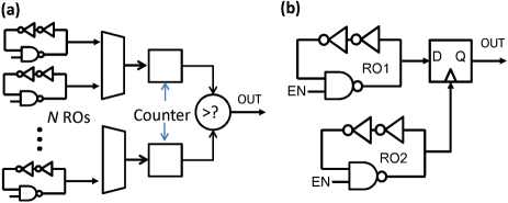
In order to connect a huge number of devices as the Internet of Things (IoT) IoT , individual devices have to be manufactured at a low cost. This has also led to the technical issue of providing an inexpensive secure ID function in each device. Thus, research and development has focused on using the variability in each individual device as the chip fingerprint. A physically unclonable function (PUF) is considered to be one of the mechanisms of protecting personal information by providing a unique ID for each device at a low cost. In the authentication process by a server, a PUF outputs a response ID to a challenge signal from the server. If the PUF output is identified as the preregistered ID, the local device is authenticated. The origins of the PUF signal come from process variations of transistors and circuits. As transistor size has shrunk, various kinds of variation have emerged, resulting in an increasing number of proposals of many types of PUFarbiter ; Lee ; Guajardo ; Holcomb ; Kim ; Marukame ; Takaya ; Takaya1 ; RRAM ; Xie ; Chen ; Suh ; Maiti0 ; Maiti1 ; Merli ; Habib ; Yin ; Fischer ; butterfly ; FF-PUF ; Yamamoto . In particular, the PUF using ring oscillators (ROs) Suh has an advantage in that it can be implemented in commercial field-programmable gate arrays (FPGAs) without difficulty and its stability is proven Maiti0 ; Merli ; Yin . However, previous RO-PUFs using the frequency difference between RO pairs [Fig. 1(a)] have disadvantages: the number of RO pairs corresponds to the length of the ID, with the result that a large number of ROs are required, and a continuous running of RO is undesirable from the viewpoint of power consumption. For example, Suh and Devadas Suh estimated that 128 pairs of oscillators (256 oscillators total) are required to generate 128 independent bits. In this study, we provide an RO-PUF using the waveform of ROs based on conventional 65 nm CMOS technology. The output waveform of ROs changes depending on each chip and provides a long ID by a single pair of ROs. Since the PUF ID is obtained after a couple of RO cycles, low power consumption is realized. Recently, in Ref. tanaCASII we have reported the implementation of a similar type of RO-PUF in commercial FPGA boards. Because the placement and routing of circuits are automatically carried out, the circuit elements are arranged at a considerable distance from each other in FPGA. Thus, the PUF circuit cannot avoid inclusion of a noisy global wiring. In ASIC devices, we can arrange the PUF circuit such that circuit elements are arranged in close proximity to each other to reduce unexpected noises. Here, we have designed the PUF circuits with a custom layout using standard logic cells, and found that the PUF performance is improved by ASIC chips. We also investigated the coupling effects of ROs in our PUF circuit.
The remainder of this paper is organized as follows: in Sect. 2, we describe our proposal of an RO-PUF using initial waveforms of ring oscillators. In Sect. 3, we present our experimental results of an RO-PUF based on 65 nm CMOS chips. In Sect. 4, we estimate the PUF performance quantitatively. Our conclusions are summarized in Sect. 5.
II PUF using waveform of ROs
II.1 Proposed PUF using waveform of ROs
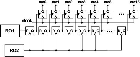
The origin of a PUF is the process variation of transistors and circuits, and the previously proposed RO-PUFs show that process variations appear in the frequency of ROs Suh . The frequency difference among different ROs means that the period of one cycle between rising edges differs depending on each RO. Thus, it is natural to consider that the waveform difference of an RO can be used as the source of a PUF (wRO-PUF). The RO begins to oscillate when the supply voltage is applied or when the enable switch is turned on. When the initial output value of the RO is 0, the time to the first rising edge of oscillation signals differs depending on each RO. Figure 1(b) shows our proposed PUF unit consisting of two ROs. Because the frequency of RO1 (1 GHz) is much higher than the clock frequency of the conventional circuit board (50-100 MHz), in order to capture the oscillation signal of the RO1 at a higher time resolution, we use RO2 as the sampling clock of FF. Figure 2 shows the whole PUF circuit including reading FFs, where the number of FFs corresponds to the ID length. Here, experiments are carried out with 16 bits.
The mechanism of our PUF is shown in Fig. 3. When , the ROs start to oscillate from the initial value of 0. The time to the first rising edge differs depending on ROs. When the period of the waveform of RO1 is longer than that of RO2 (), the initial value of the output in Fig. 3(a) is 0. When , the initial value of the output in Fig. 3(a) is 1. This mechanism resembles that of the conventional RO-PUFs. Moreover, because the waveforms are analog data, the relative difference between two waveforms is the origin of new degrees of freedom when they are digitized. Figures 3(c) and 3(d) show examples where the output signal (OUT) pattern of the wRO-PUF changes depending on the relative change even when we limit . and for the difference, even when we limit .
II.2 Effect of coupling between two ROs
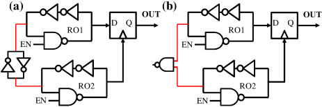
In the basic unit of our PUF [Fig. 1(b)], the relative frequency between two ROs determines the waveform of the PUF-ID. As Ref. Maneatis shows that the coupling of ROs improves the delay control, we have also implemented modified PUF circuits whose units are shown in Fig. 4. Figure 4(a) shows a PUF circuit of electrically coupled ROs, and Fig. 4(b) shows that of capacitively coupled ROs.

III PUF chip using 65 nm CMOS process
III.1 Hamming distance evaluation of RO-PUF using waveform
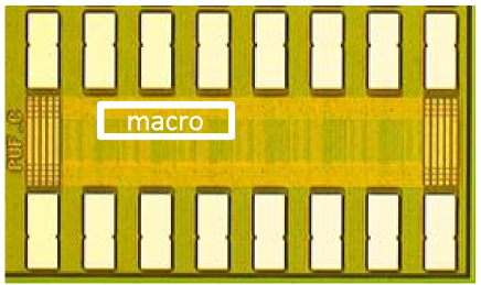
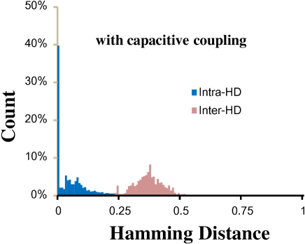
Figure 5 shows a photomicrograph of an RO-PUF chip obtained using 65 nm CMOS technology where the macrosize is 27328 m2. We measured 10 chips. ID is determined by the pattern of the wRO-PUF output that appears most frequently. The most important metric for estimating PUF performance is the Hamming distance (HD), which is the number of different bits between two outputs. The intra-HD represents the reproducibility of each chip, and the inter-HD represents the uniqueness between different chips. A sharp distribution at around HD=0 and a sufficient gap between the intra-HD and the inter-HD indicate the ideal HD distribution. The ideal inter-HD is distributed around half of the ID length.
First, let us show the result of the modified PUF in Fig. 4. It is found that the RO-PUF formed by cross-coupled inverters [Fig. 4(a)] only output fixed values and did not work as a PUF. This shows that this coupling is very strong for detecting the variation of the PUF output. Figure 6 shows the measured results for the modified PUF circuit in Fig. 4(b). Here, samplings are carried out by repeating and . Figure 6 shows that the intra-HD of the wRO-PUF with a capacitive coupling is not ideal because the result indicated that the same ID is not always produced with a high probability.
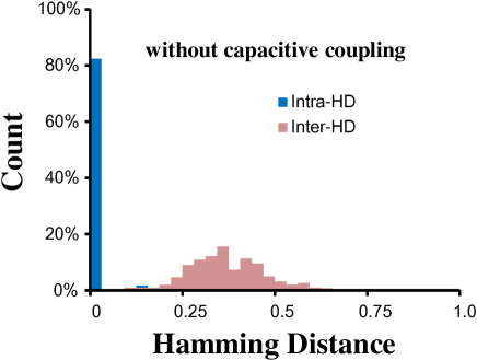
Figure 7 shows the result of the HD in Fig. 2. We can see that the identification of each chip is excellent (HD=0) and well distinct from those of the other chips. These results show that the simplest form of the wRO-PUF is the best form of the wRO-PUF.
III.2 Voltage dependence
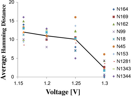
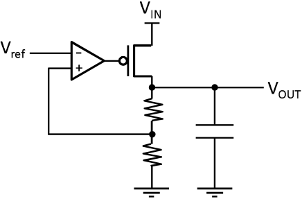
As shown in Ref. Sayed , RO frequency changes as the physical environment changes. Figure 8 shows the shift of the average Hamming distance estimated from a 1.3 V operation over ten chips of the wRO-PUF without coupling. We can see a linear dependence between the voltage difference and the shift in the average Hamming distance. This is the same tendency as the temperature dependence shown in Ref. Sayed . Because the ID should be unique, a change of the ID is undesirable. To solve this problem, we can utilize the linear dependence of the voltage during the ID shift by monitoring voltage. That is, the ID is corrected depending on the difference in the measured voltage from the reference voltage. Otherwise, a feedback circuit for stabilizing the supply voltage will be required Miliken . Figure 9 shows a schematic of a typical voltage regulator. Because the change in frequency depending on the change in voltage is a general aspect of an RO-PUF, these kinds of additional circuits will be required in other conventional RO-PUF circuits. In any event, this is a problem to be addressed in future studies.
III.3 Comparison with previous RO-PUFs
We would like to quantitatively compare our RO-PUF with the previously proposed RO-PUF Suh . First, let us compare the areas of both PUFs, when 128 bit outputs are required. For our wRO-PUF circuit, we prepare two sets of RO pairs [Fig. 2], each of which outputs more than 64 bits. Then, our wRO-PUF has 4 ROs and 64 (=) FFs. If each RO has 20 transistors, and 30 transistors are used for each FF, about 2000 transistors are present in our wRO-PUF circuit. If we reduce the number of FFs, which dominate the area of our wRO-PUF, we can further reduce the area of our circuit. Suh and Devadas Suh showed that 35 ROs are used to obtain 133 bits. Their typical RO-PUF has two MUXs, two counters, and a comparison circuit. When we assume that each MUX consists of combined 4-input MUXs, each of which has about 30 transistors, 21 (=16+4+1) 4-input MUXs are required, resulting in 1260 transistors for the MUX parts. If 16 bit counters are used, 32 FFs with additional circuits are required, resulting in 960 transistors being present in this part. When full adders are used to compare two RO outputs, and each full adder has 20 transistors, there are 320 transistors. Thus, the previously proposed PUF has about 3240 transistors (Table I).
Next, let us compare power consumptions. For the previous PUF in Ref. Suh , 16 bit counters are operated to obtain a bit. Therefore, the previous RO-PUF has to run an RO pair for at least 2048 (=) cycles of the system clock. In contrast, an RO pair of our wRO-PUF acquires 16 bits during a cycle of the system clock. Thus, the RO pair should run only 8 (=128/16) clocks in our wRO-PUF, resulting in a great reduction in power (Table I).
Table I. Comparison of area (number of transistors) and clock cycle (128 bit output) . Area Clock cycle Our wRO-PUF 2000 8 Previous RO-PUF 3240 2048
IV PUF performance evaluation
We evaluate the PUF performance of our wRO-PUF on the basis of the metrics discussed in Refs. Maiti3 and Hori . The results of the evaluation with and without coupling are shown in Table II. Here, uniqueness is calculated using
| (1) |
where is the number of tested chips, is the length of the ID, and is the ID pattern that appears most frequently. The reliability of the -th chip is calculated using
| (2) |
where is the number of times that sampling is done and is the -th output. Uniformity is calculated using
| (3) |
where is the -th binary bit of an -th response from a chip . We average Uniformityi,n over many responses. The average results over all samples are listed in Table II.
It seems that the results shown in Table II are inferior to those shown in Refs. Maiti3 and Hori . This is considered to be because the number of ROs is much smaller than those in the literature. Here, the number of RO pairs in the coupling case is four and that in the case without coupling is one. In general, as the number of ROs increases, these metrics are considered to improve, because the complexity increases as the number of ROs increases. The PUF performance of an RO pair in the present ASIC chip seems to be better than that of FPGA. Therefore, two or three RO pairs will improve the PUF performance. Thus, from these results, we can see the original properties of our RO-PUF. The effect of coupling can be seen in the uniqueness estimation. The uniqueness of our wRO-PUF without coupling is close to the ideal value, resulting in the excellent performance of our wRO-PUF without coupling. In any event, the improvement in PUF performance is a future problem.
Table II. PUF performance measured on the two types of chip (in %). With coupling Without coupling Ideal value Uniformity 40.82 38.75 50 Reliability 94.67 94.48 100 Uniqueness 37.22 48.81 50
V Conclusions
We proposed an RO-PUF using the initial waveform (wRO-PUF) based on a 65 nm CMOS circuit. The initial waveform of an RO is effectively sampled by other ROs. No coupling between two ROs is required. The simple circuit [Figs. 1(b) and 2] is proved to be best for the PUF-ID. Compared with the conventional RO-PUF using a frequency difference, a small number of ROs are used with a couple of system clock operations, resulting in a low power consumption and a small area.
Acknowledgements.
T.T. thanks A. Nishiyama, M. Koyama, K. Muraoka, S. Shimizu, Y. Komano, H. Noguchi, T. Kanesige, T. Ootuki, and T. Yamakawa for helpful discussions.References
- (1) X. Liu, J. Zhou, C. Wang, K. Chang, J. Lan, L. Liao, Y. Lam, Y. Yang, B. Wang, X. Zhang, W. Goh, T. Kim, and M. Je, IEEE Trans. Circuits Syst. II, 62, 1149 (2015).
- (2) D. Lim, J. Lee, B. Gassend, G. E. Suh, M. van Dijk, and S. Devadas, IEEE Trans.VLSI Syst. 13, 1200 (2005).
- (3) J. W. Lee, D. Lim, B. Gassend, G. E. Suh, M. van Dijk, and S. Devadas, IEEE Symp. VLSI Circuits, 2004, p. 176.
- (4) J. Guajardo, S. S. Kumar, G.-J. Schrijen, and P. Tuyls, 9th Int. Workshop Cryptographic Hardware and Embedded Systems (CHES’07), 2007, p. 63.
- (5) D. E. Holcomb, W. P. Burleson, and K. Fu, IEEE Trans. Comput. 58, 1198 (2009).
- (6) M. S. Kim, D. I. Moon, S. K. Yoo, and S. H. Lee, IEEE Trans. Nanotechnol. 14, 384 (2015).
- (7) T. Marukame, T. Tanamoto, and Y. Mitani, IEEE Trans. Magn. 50, 1 (2014).
- (8) S. Takaya, T. Tanamoto, H. Noguchi, K. Ikegami, K. Abe, and S. Fujita, Ext. Abstr. Int. Conf. Solid State Devices and Materials (SSDM2016), 2016, B-2-05.
- (9) S. Takaya, T. Tanamoto, H. Noguchi, K. Ikegami, K. Abe, and S. Fujita, to be published in Jpn. J. Appl. Phys. (SS16089)
- (10) A. Chen, IEEE Electron Device Lett. 36, 138 (2015).
- (11) Y. Xie, X. Xue, J. Yang, Y. Lin, Q. Zou, R. Huang, and J. Wu, IEEE Trans. Circuits Syst. II, 63, 336 (2015).
- (12) J. Chen, T. Tanamoto, H. Noguchi, and Y. Mitani, IEEE Symp. VLSI Technology, 2015, p. 40.
- (13) G. E. Suh and S. Devadas, 44th Ann. Design Automation Conf. (DAC’07), 2007, p. 9.
- (14) A. Maiti, J. Casarona, L. McHale, and P. Schaumont, IEEE Symp. Hardware-Oriented Security and Trust (HOST), 2010, p. 94.
- (15) A. Maiti and P. Schaumont, 19th Int. Conf. Field Programmable Logic and Applications (FPL’09), 2009, p. 703.
- (16) D. Merli, F. Stumpf, and C. Eckert, 5th Workshop Embedded Systems Security (WESS’ 10), 2010.
- (17) B. Habib, K. Gaj, and J.P. Kaps, Euromicro Conf. Digital System Design (DSD’13), 2013, p. 697.
- (18) C.-E. Yin and G. Qu, IEEE Symp. Hardware-Oriented Security and Trust (HOST), 2010, p. 100.
- (19) L. Bossuet, X. T. Ngo, Z. Cherif, and V. Fischer, IEEE Trans. Emerging Top. Comput. 2, 30 (2014).
- (20) S. Kumar, J. Guajardo, R. Maes, G.-J. Schrijen, and P. Tuyls, IEEE Symp. Hardware-Oriented Security and Trust (HOST 2008), 2008, p. 67.
- (21) R. Maes, P. Tuyls, and I. Verbauwhede, Workshop Information and System Security (WISSec), 2008, p. 17.
- (22) D. Yamamoto, K. Sakiyama, M. Iwamoto, K. Ohta, T. Ochiai, M. Takenaka, and K. Itoh, 13th Int. Workshop Cryptographic Hardware and Embedded Systems (CHES’11), 2011, p390.
- (23) T. Tanamoto, S. Yasuda, S. Takaya, and S. Fujita, to be published in IEEE Trans. Circuits Syst. II.
- (24) J. G. Maneatis and M.A. Horowitz, IEEE J. Solid-State Circuits 28, 1273 (1993).
- (25) M. A. Sayed, and P. H. Jones, IEEE Int. Conf. Reconfigurable Computing and FPGAs (ReConFig2011), 2011, p. 92.
- (26) R. J. Milliken, J. Silva-Martínez, and E. Sánchez-Sinencio, IEEE Trans. Circuits Syst. I 54, 1879 (2007).
- (27) A. Maiti and P. Schaumont, IEEE Trans. VLSI Syst., 22, 1854 (2013).
- (28) Y. Hori, T. Yoshida, T. Katashita, and A. Satoh, IEEE Int. Conf. Reconfigurable Computing and FPGAs (ReConFig2010), 2010, p. 298.