Present Address: ]Department of Precision Science and Technology, Graduate School of Engineering, Osaka University, Osaka 565-0871, Japan
Origins of the structural phase transitions in MoTe2 and WTe2
Abstract
Layered transition metal dichalcogenides MoTe2 and WTe2 share almost similar lattice constants as well as topological electronic properties except their structural phase transitions. While the former shows a first-order phase transition between monoclinic and orthorhombic structures, the latter does not. Using a recently proposed van der Waals density functional method, we investigate structural stability of the two materials and uncover that the disparate phase transitions originate from delicate differences between their interlayer bonding states near the Fermi energy. By exploiting the relation between the structural phase transitions and the low energy electronic properties, we show that a charge doping can control the transition substantially, thereby suggesting a way to stabilize or to eliminate their topological electronic energy bands.
pacs:
73.22.-f, 71.15.Mb, 64.70.NdSince the successful exfoliation of various two dimensional (2D) crystals in 2005 Novoselov et al. (2005), the layered materials in a single layer as well as bulk forms have attracted serious attention owing to their versatile physical properties Gupta et al. (2015); Geim and Grigorieva (2013). Among them, the layered transition metal dichalcogenides (TMDs) show various interesting electronic properties such as type-II Weyl semimetallic (WSM) energy bands Soluyanov et al. (2015), gate dependent collective phenomena Ye et al. (2012); Yu et al. (2015), and quantum spin Hall (QSH) insulating state Qian et al. (2014) to name a few.
Because of the layered structures of TMDs, several polymorphs can exist and show characteristic physical properties depending on their structures Kolobov and Tominaga (2016). A typical TMD shows the trigonal prismatic (2) or the octahedral (1) structures Mak et al. (2010); Wang et al. (2012); Mattheiss (1973); Wilson and Yoffe (1969). For MoTe2 and WTe2, the 2 structure (-phase, 63/) is a stable semiconductor while the 1 form is unstable Qian et al. (2014); Keum et al. (2015). The unstable 1 structure turns into the distorted octahedral one (1) Eda et al. (2012); Qian et al. (2014). The stacked 1 single layer forms a three-dimensional bulk with the monoclinic structure (-phase, 21/) or the orthorhombic one (-phase, 21) (see Fig. 1) Brown (1966); Dawson and Bullet (1987); Mar et al. (1992). Interestingly, the phase with a few layers is a potential candidate of QSH insulator Qian et al. (2014) and the bulk phase shows type-II Weyl semimetalic energy bands Sun et al. (2015); Soluyanov et al. (2015); Chang et al. (2016), respectively. Since the structural differences between and phases are minute (4∘ tilting of axis along out-of-plane direction in phase with respect to one in phase), the sensitive change in their topological low energy electronic properties is remarkable and the transition between different structures can lead to alternation of topological properties of the system.
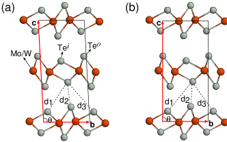
A phase transition between the - and -phase in the layered TMDs has been known for a long time Clarke et al. (1978); Dawson and Bullet (1987). MoTe2 shows a first-order transition from the - to -structure at around 250 K Clarke et al. (1978) when temperature decreases. WTe2, however, does not show any transition and stays at the -phase Kang et al. (2015); Pan et al. (2015). Since the structural parameters of a single layer of 1-MoTe2 and 1-WTe2 are almost the same Brown (1966); Mar et al. (1992); Choe et al. (2016) and Mo and W belong to the same group in the periodic table, the different phase transition behaviors are intriguing and origins of the contrasting features are yet to be clarified.
To understand the phase transition, the proper treatment of long and short range interlayer interaction in TMDs is essential. Most of the theoretical studies, however, fail to reproduce the experimental crystal structures of the two phases of MoTe2 and WTe2 so do their topological electronic structures using crystal structures obtained from calculations Lee et al. (2015); Zhao et al. (2015); Lv et al. (2015); Homes et al. (2015); Liu et al. (2016); Qi et al. (2016); Lu et al. (2016). Instead, the atomic structures from experiment data are routinely used to understand and predict the low energy electronic properties Soluyanov et al. (2015); Sun et al. (2015); Wang et al. (2016); Tamai et al. (2016); Deng et al. (2016); Huang et al. (2016); Bruno et al. (2016). This is because the calculated lattice parameters, especially interlayer distance, by using the conventional first-principles calculations Lee et al. (2015); Zhao et al. (2015); Chang et al. (2016); sup [even with advanced empirical van der Waals (vdW) interaction correction schemes Qi et al. (2016); sup ; Lee et al. (2015)] hardly reproduce the observed distances. Since the interlayer interaction governs the phase transition as well as structural properties, a successful description of interlayer interactions is required to understand or predict electronic structures and topological properties. Motivated by the current situation of experiment and theoretical studies, we perform calculations using a new vdW density functional method for the interlayer interaction Hamada (2014) and analyze the existence and absence of the first-order structural phase transition related with various low energy topological electronic properties of MoTe2 and WTe2.
Here we first compute crystal structures of the both compounds based on an advanced self-consistent density functional method for the vdW interaction Hamada (2014) and obtain the best agreement with the available crystal structures in experiments. Then we show theoretically that MoTe2 and WTe2 have distinct structural phase transitions because their interlayer bondings differ depending on valence electron configurations of transition metals. A critical role of low energy electronic states for crystal symmetry is further demonstrated by showing that an external charge doping can alter the structural phase transition significantly. From this, our results in this Rapid Communication can provide a firm computational and theoretical basis for future development in discovering and engineering various topological electronic states in layered materials.
Our ab initio calculation method employs the projector-augmented wave method Blöchl (1994) as implemented in the Vienna Ab-initio Simulation Package () Kresse and Hafner (1993); Kresse and Furthmüller (1996). We use the plane-wave cutoff of 450 eV and the 32168 Monkhorst-Pack meshes for the Brillouin zone integration to achieve the convergence criterion of 0.1 meV in total energy difference () between and phase. The spin-orbit coupling (SOC) effect is included in all calculations and on-site Coulomb repulsion () Dudarev et al. (1998) is considered for the specific cases. These parameters are fully tested to achieve a desired accuracy for the calculations, and the energy and force are converged with thresholds of 10-6 eV and 510-3 eV/Å, respectively. On top of the conventional calculation method, we use a vdW density functional (rev-vdW-DF2) method which is recently proposed by one of the authors Hamada (2014), where the revised Becke exchange functional (B86R) Becke (1986) is adopted for exchange functional together with the second version of nonlocal vdW-DF (vdW-DF2) Dion et al. (2004); *Dion2004e; Lee et al. (2010) as a nonlocal correlation. The rev-vdW-DF2 improves the description of the attractive vdW interaction resulting in the most accurate interlayer distances of layered materials over the various other vdW calculation methods sup ; Björkman (2014); Peng et al. (2016). The electron and hole dopings are simulated by adding and removing the electron and the background charge is added to keep the charge neutrality. To evaluate the vibrational energy and entropy, we use the harmonic approximation as implemented in PHONOPY package Togo and Tanaka (2015) where the vibrational frequencies are obtained from the force constant matrix of the fully relaxed geometries using numerical derivatives of the rev-vdW-DF2 energies.
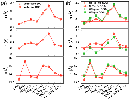
The atomic structures obtained from our calculation match the available experiment data very well. The calculated structural parameters of MoTe2 in the phase (hereafter called -MoTe2) are summarized in Fig. 2 (a) and those for MoTe2 and WTe2 in the phase (-MoTe2 and -WTe2) are summarized in Fig. 2 (b) (see also Tables SI and SII sup ). The comparison between the optimized lattice parameters using the various vdW functionals and experiment data for the and phases are also illustrated, respectively. We note that the inclusion of SOC improves the accuracy marginally (see Fig. 2, Tables SI and SII sup ). Among the various vdW correction schemes, we found that the rev-vdW-DF2 outperforms several other functionals. The calculated equilibrium unit cell volume using our method yields 306.5 Å3 for the -MoTe2 and 307.0 and 312.1 Å3 for the -MoTe2 and -WTe2, respectively, in very good agreement with experimental value of 303.6, 305.9, and 306.6 Å3, respectively. These are only larger by 1.0, 0.4, and 1.8 than those from experiment, respectively. From the fully optimized structures for both phases, we find that the shortest interlayer distance between Te atoms (denoted by in Fig. 1) changes negligibly between the two phases while other distances ( and ) vary significantly (see Fig. 1 and Table SIII sup ).
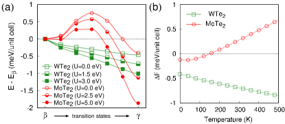
As the temperature increases, the stable -MoTe2 at the low temperature undergoes a first-order phase transition to the phase Clarke et al. (1978); Dawson and Bullet (1987); Mar et al. (1992) while WTe2 stays in the phase Kang et al. (2015); Pan et al. (2015). These observations are consistent with our total energy calculation including the vdW interaction. We found that the phase is energetically more stable than the phase by = 0.40 and 0.46 meV per unit cell for MoTe2 and WTe2, respectively, in good agreement with recent other studies Qi et al. (2016); Lu et al. (2016). For MoTe2, the transition state is unstable by 0.75 and 1.15 meV per unit cell than the - and -phase, respectively, indicating -MoTe2 is metastable state, while WTe2 shows no energy barrier, implying that -WTe2 does not exist [see Fig. 3(a)]. An atomic structure of the hypothetical -WTe2 is assumed to follow -MoTe2. We also calculated the free energy of each system without and found that the structural phase transition occurs at around 150 K for MoTe2 and no transition for WTe2, compatible with the experiment [Fig. 3(b)].
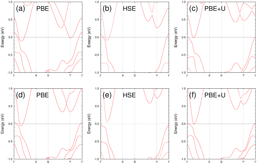
Recent studies Keum et al. (2015); Zheng et al. (2016) show that the insulating behavior of a few layers of MoTe2 and WTe2 are not described well within the mean-field treatment of Coulomb interactions. This implies a critical effect of many-body interaction. Thus, we further add the local Coulomb repulsion of on top of our rev-vdW-DF2 method to reproduce the finite energy band gap obtained from previous hybrid density functional calculations Keum et al. (2015); sup . We set to be 5.0 and 3.0 eV for Mo 4 and W 5 orbitals, respectively sup and obtain further increasing = 1.9 and 1.0 meV per unit cell for MoTe2 and WTe2, respectively. We note that inclusion of stabilizes the phase of both materials while the transition energy barrier for MoTe2 decreases with increasing [Fig. 3(a)].
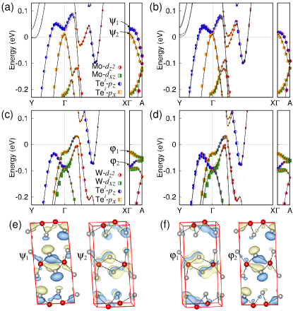
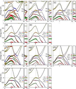
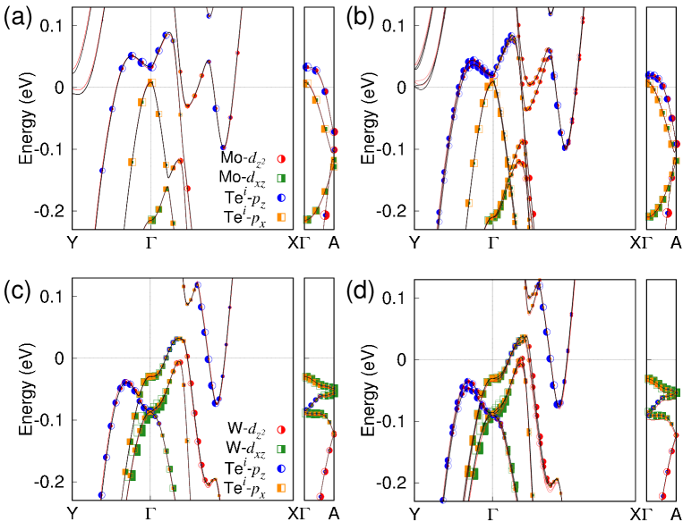
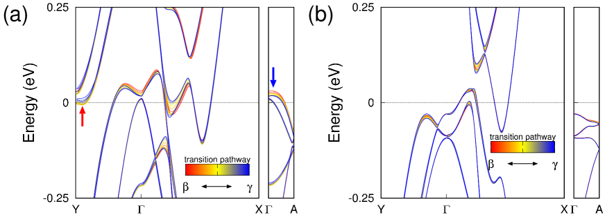
In Fig. 4, we show the low energy electronic bands near the Fermi energy () for two different phases of MoTe2 and WTe2, respectively. We first find that the two compounds show the markedly different band dispersion along the - direction. For MoTe2, the topmost partially occupied valence band state [denoted by in Figs. 4(a) and 4(e)] is mainly an antibonding state along the direction (see Fig. 1) between the hybridized states of orbital of the lower Te atom (denoted by Tei in Fig. 1) and orbital of Mo. The next valence band state [ in Fig. 4(a)] is mainly an antibonding state between the hybridized states of orbital of Tei and orbital of Mo [Fig. 4(e)]. We also note that, in the first two valence bands, contribution of orbitals of Teo (see Fig. 1) is relatively smaller than those of Tei. In contrast to the case of MoTe2, the topmost valence state [ state in Figs. 4(c) and 4(f)] of WTe2 is similar to the second valence state () of MoTe2 and vice versa [Fig. 4(f)]. Because of the different atomic orbital configurations between Mo ([Kr]5s14d5) and W atom ([Xe]6s24f145d4), those two valence bands of WTe2 are fully occupied along the - and - direction [Figs. 4(b) and 4(d)] while those of MoTe2 are partially occupied along all directions [Figs. 4(a) and 4(c)]. The estimated band width along - for those two bands of MoTe2 is four times larger than the width of WTe2. These apparent differences between the two compounds are found to originate from the fact that WTe2 has a quite smaller contribution of orbital of Te atoms to the first two valence states compared to that of MoTe2 (Fig. S2 sup ]). We also calculated the whole band structures again using a semilocal correlational functional (Fig. S3 sup ) instead of the rev-vdW-DF2 while keeping the fully relaxed atomic structures to check the effect of vdW functional on the energy band structures. Changes in the band structures are found to be minimal agreeing with previous studies Thonhauser et al. (2007); Hamada and Yanagisawa (2011).
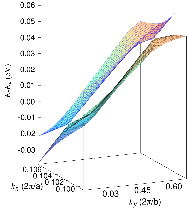
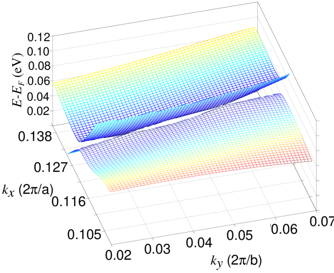
Since the calculated total energy difference between the two phases is very small, we do not expect significant changes between energy bands of different phases. Indeed, as shown in Figs. 4 and S4 sup , there are little modifications in the band structures between the two phases of MoTe2 (WTe2) except that all bands in the phase split into spin-polarized ones in the phase due to its broken inversion symmetry. However, in MoTe2, there is a small but important variation in the band structures with the transition: The partially occupied valence bands related with the interlayer antibonding states ( and ) in the -MoTe2 move down in energy (are steadily occupied) along the transition pathway to the -MoTe2 while the corresponding states in the -WTe2 does not (Figs. 4 and S4 sup ). The increase in the occupancies in the first two valence bands stabilize the antibonding states along the elongated distance of Kim et al. (2015). This is made possible because there is a net charge transfer from the intralayer bonding states around the -point to the interlayer anti-bonding states near the as shown in Fig. S4 sup . This costs energy and explains the metastability of the -MoTe2. Since those bands in WTe2 are all occupied, there is no metastable phase for the WTe2.
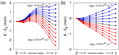
Considering the crucial role of occupancy of the interlayer bonding states near the , we expect that the external doping can control the structural phase transition. Indeed, we find that the hole (electron) doping can stabilize the () phase of both compounds as shown in Fig. 5. The amount of doping density that is necessary to invert the direction of phase transition is about 1.01020 cm-3. We note that few recent experiments Ye et al. (2012); Yu et al. (2015) can achieve such a level of doping for thin TMD flakes. It is anticipated that the - charge or hole injection can turn on and off QSH insulating phase and WSM states, respectively. We also note that only electron doping can push the to the Weyl points of WSM states because hole doping destroys the phase.
Lastly, we comment on the existence of Weyl points calculated from our atomic structures of both compounds. For -MoTe2 and -WTe2, all the bands are split into spin polarized ones thanks to the broken inversion symmetry and SOC [Figs. 4(b) and 4(d)]. As already shown by other studies Sun et al. (2015); Tamai et al. (2016), we also find eight Weyl points of -MoTe2 in the = 0 plane (see Fig. S5 sup ). Unlike the robust Weyl points in -MoTe2, the slight overestimation of and axes (by 0.5 and 1.0) in our calculation for -WTe2 [see Fig. 2(b)] merges the topological Weyl points with the opposite chiralities Soluyanov et al. (2015), highlighting their sensitivity on the detailed structure parameters. We can recover the eight Weyl points in the = 0 plane of -WTe2 under biaxial strain ( and ) of 1.5 (see Fig. S6 sup ).
In conclusion, using an advanced calculation method for the vdW interaction, we computed accurate lattice structures of MoTe2 and WTe2 and uncovered origins of their disparate structural phase transition phenomena. We showed that the slight differences in low energy states related with the interlayer bondings are shown to be pivotal in determining the symmetry of bulk crystals. Since the structural transition intertwines their QSH phase and WSM states, our results shed light onto understanding delicate interplay between topological electronic properties and crystal structures. Furthermore, we find that the electron and hole doping alter the structural phase transitions, opening a way to control the topological electronic properties of layered TMDs using available experiment techniques.
We thank Dr. Jun-Ho Lee for fruitful discussions at an early stage of this work. Y.-W.S. was supported by the National Re- search Foundation of Korea funded by the Ministry of Science, ICT and Future Planning of Korean government (QMMRC, No, R11-2008-053-01002-0). The computing resources were supported by the Center for Advanced Computation (CAC) of KIAS.
References
- Novoselov et al. (2005) K. Novoselov, D. Jiang, F. Schedin, T. Booth, V. Khotkevich, S. Morozov, and A. Geim, Proc. Natl. Acad. Sci. USA 102, 10451 (2005).
- Gupta et al. (2015) A. Gupta, T. Sakthivel, and S. Seal, Prog. Mater. Sci. 73, 44 (2015).
- Geim and Grigorieva (2013) A. K. Geim and I. V. Grigorieva, Nature (London) 499, 419 (2013).
- Soluyanov et al. (2015) A. A. Soluyanov, D. Gresch, Z. Wang, Q. Wu, M. Troyer, X. Dai, and A. Bernevig, Nature 527, 495 (2015).
- Ye et al. (2012) J. T. Ye, Y. J. Zhang, R. Akashi, M. S. Bahramy, R. Arita, and Y. Iwasa, Science 338, 1193 (2012).
- Yu et al. (2015) Y. Yu, F. Yang, X. F. Lu, Y. J. Yan, Y.-H. Cho, L. Ma, X. Niu, S. Kim, Y.-W. Son, D. Feng, S. Li, S.-W. Cheng, X. H. Chen, and Y. Zhang, Nat. Nanotech. 10, 270 (2015).
- Qian et al. (2014) X. Qian, J. Liu, L. Fu, and J. Li, Science 346, 1344 (2014).
- Kolobov and Tominaga (2016) A. V. Kolobov and J. Tominaga, Two-Dimensional Transition-Metal Dichalcogenides, Vol. 239 (Springer, Berlin, 2016).
- Mak et al. (2010) K. F. Mak, C. Lee, J. Hone, J. Shan, and T. F. Heinz, Phys. Rev. Lett. 105, 136805 (2010).
- Wang et al. (2012) Q. H. Wang, K. Kalantar-Zadeh, A. Kis, J. N. Coleman, and M. S. Strano, Nat. Nanotechnol. 7, 699 (2012).
- Mattheiss (1973) L. F. Mattheiss, Phys. Rev. B 8, 3719 (1973).
- Wilson and Yoffe (1969) J. A. Wilson and A. D. Yoffe, Adv. Phys. 18, 193 (1969).
- Keum et al. (2015) D. H. Keum, S. Cho, J. H. Kim, D.-H. Choe, H.-J. Sung, M. Kan, H. Kang, J.-Y. Hwang, S. W. Kim, H. Yang, K. J. Chang, and Y. H. Lee, Nat. Phys. 11, 482 (2015).
- Eda et al. (2012) G. Eda, T. Fujita, H. Yamaguchi, D. Voiry, M. Chen, and M. Chhowalla, ACS Nano 6, 7311 (2012).
- Brown (1966) B. E. Brown, Acta Crystallogr. 20, 268 (1966).
- Dawson and Bullet (1987) W. G. Dawson and D. W. Bullet, J. Phys. C: Sol. Stat. Phys. 20, 6159 (1987).
- Mar et al. (1992) A. Mar, S. Jobic, and J. A. Ibers, J. Am. Chem. Soc. 114, 8963 (1992).
- Sun et al. (2015) Y. Sun, S.-C. Wu, M. N. Ali, C. Felser, and B. Yan, Phys. Rev. B 92, 161107 (2015).
- Chang et al. (2016) T.-R. Chang, S.-Y. Xu, G. Chang, C.-C. Lee, S.-M. Huang, B. Wang, G. Bian, H. Zheng, D. S. Sanchez, I. Belopolski, N. Alidoust, M. Neupane, A. Bansil, H.-T. Jeng, H. Lin, and M. Z. Hasan, Nat. Commun. 7, 10639 (2016).
- Clarke et al. (1978) R. Clarke, E. Marseglia, and H. Hughes, Phil. Mag. B 38, 121 (1978).
- Kang et al. (2015) D. Kang, Y. Zhou, W. Yi, C. Yang, J. Gou, Y. Shi, S. Zhang, Z. Wang, C. Zhang, S. Jiang, A. Li, K. Yang, Q. Wu, G. Zhang, L. Sun, and Z. Zhao, Nat. Commun. 6, 7804 (2015).
- Pan et al. (2015) X.-C. Pan, X. Chen, H. Liu, Y. Feng, Z. Wei, Y. Zhou, Z. Chi, L. Pi, F. Yen, F. Song, X. Wan, Z. Yang, B. Wang, G. Wang, and Y. Zhang, Nat. Commun. 6, 7805 (2015).
- Choe et al. (2016) D.-H. Choe, H.-J. Sung, and K. J. Chang, Phys. Rev. B 93, 125109 (2016).
- Lee et al. (2015) C.-H. Lee, E. Cruz-Silva, L. Calderin, H. M. J. Nguyen, M., B. Bersch, T. E. Mallouk, and J. A. Robinson, Sci. Rep. 5, 10013 (2015).
- Zhao et al. (2015) Y. Zhao, H. Liu, J. Yan, W. An, J. Liu, X. Zhang, H. Wang, Y. Liu, H. Jiang, Q. Li, Y. Wang, X.-Z. Li, D. Mandrus, X. C. Xie, M. Pan, and J. Wang, Phys. Rev. B 92, 041104 (2015).
- Lv et al. (2015) H. Y. Lv, W. J. Lu, D. F. Shao, Y. Liu, S. G. Tan, and Y. P. Sun, Europhys. Lett. 110, 37004 (2015).
- Homes et al. (2015) C. C. Homes, M. N. Ali, and R. J. Cava, Phys. Rev. B 92, 161109 (2015).
- Liu et al. (2016) G. Liu, H. Y. Sun, J. Zhou, Q. F. Li, and X.-G. Wan, New J. Phys. 18, 033017 (2016).
- Qi et al. (2016) Y. Qi, P. G. Naumov, M. N. Ali, C. R. Rajamathi, W. Schnelle, O. Barkalov, M. Hanfland, S.-C. Wu, C. Shekhar, Y. Sun, V. Süß, M. Schmidt, U. Schwarz, E. Pippel, P. Werner, R. Hillebrand, T. Förster, E. Kampert, S. Parkin, R. J. Cava, C. Felser, B. Yan, and S. A. Medvedev, Nat. Commun. 7, 11038 (2016).
- Lu et al. (2016) P. Lu, J.-S. Kim, J. Yang, H. Gao, J. Wu, D. Shao, B. Li, D. Zhou, J. Sun, D. Akinwande, D. Xing, and J.-F. Lin, Phys. Rev. B 94, 224512 (2016).
- Wang et al. (2016) Z. Wang, D. Gresch, A. A. Soluyanov, W. Xie, S. Kushwaha, X. Dai, M. Troyer, R. J. Cava, and B. A. Bernevig, Phys. Rev. Lett. 117, 056805 (2016).
- Tamai et al. (2016) A. Tamai, Q. S. Wu, I. Cucchi, F. Y. Bruno, S. Riccò, T. K. Kim, M. Hoesch, C. Barreteau, E. Giannini, C. Besnard, A. A. Soluyanov, and F. Baumberger, Phys. Rev. X 6, 031021 (2016).
- Deng et al. (2016) K. Deng, G. Wan, P. Deng, K. Zhang, S. Ding, E. Wang, M. Yan, H. Huang, H. Zhang, Z. Xu, J. Denlinger, A. Fedorov, H. Yang, W. Duan, H. Yao, Y. Wu, S. Fan, H. Zhang, X. Chen, and S. Zhou, Nat. Phys. 12, 1105 (2016).
- Huang et al. (2016) L. Huang, T. M. McCormick, M. Ochi, Z. Zhao, M.-T. Suzuki, R. Arita, Y. Wu, D. Mou, H. Cao, J. Yan, N. Trivedi, and A. Kaminski, Nat. Mater. 15, 1155 (2016).
- Bruno et al. (2016) F. Y. Bruno, A. Tamai, Q. S. Wu, I. Cucchi, C. Barreteau, A. de la Torre, S. McKeown Walker, S. Riccò, Z. Wang, T. K. Kim, M. Hoesch, M. Shi, N. C. Plumb, E. Giannini, A. A. Soluyanov, and F. Baumberger, Phys. Rev. B 94, 121112 (2016).
- (36) See Supplemental Material at http://link.aps.org/supplemental for the details of geometrical parameters and band structures.
- Hamada (2014) I. Hamada, Phys. Rev. B 89, 121103 (2014).
- Blöchl (1994) P. E. Blöchl, Phys. Rev. B 50, 17953 (1994).
- Kresse and Hafner (1993) G. Kresse and J. Hafner, Phys. Rev. B 48, 13115 (1993).
- Kresse and Furthmüller (1996) G. Kresse and Furthmüller, Comput. Mater. Sci. 6, 15 (1996).
- Dudarev et al. (1998) S. L. Dudarev, G. A. Botton, S. Y. Savrasov, C. J. Humphreys, and A. P. Sutton, Phys. Rev. B 57, 1505 (1998).
- Becke (1986) A. D. Becke, J. Chem. Phys. 85, 7184 (1986).
- Dion et al. (2004) M. Dion, H. Rydberg, E. Schröder, D. C. Langreth, and B. I. Lundqvist, Phys. Rev. Lett. 92, 246401 (2004).
- Dion et al. (2005) M. Dion, H. Rydberg, E. Schröder, D. C. Langreth, and B. I. Lundqvist, ibid. 95, 109902(E) (2005).
- Lee et al. (2010) K. Lee, E. D. Murray, L. Kong, B. I. Lundqvist, and D. C. Langreth, Phys. Rev. B 82, 081101 (2010).
- Björkman (2014) T. Björkman, J. Chem. Phys. 141, 074708 (2014).
- Peng et al. (2016) H. Peng, Z.-H. Yang, J. P. Perdew, and J. Sun, Phys. Rev. X 6, 041005 (2016).
- Togo and Tanaka (2015) A. Togo and I. Tanaka, Scr. Mater. 108, 1 (2015).
- Zheng et al. (2016) F. Zheng, C. Cai, S. Ge, X. Zhang, X. Liu, H. Lu, Y. Zhang, J. Qiu, T. Taniguchi, K. Watanabe, S. Jia, J. Qi, J.-H. Chen, D. Sun, and J. Feng, Adv. Mater. 28, 4845 (2016).
- Thonhauser et al. (2007) T. Thonhauser, V. R. Cooper, S. Li, A. Puzder, P. Hyldgaard, and D. C. Langreth, Phys. Rev. B 76, 125112 (2007).
- Hamada and Yanagisawa (2011) I. Hamada and S. Yanagisawa, Phys. Rev. B 84, 153104 (2011).
- Kim et al. (2015) S.-W. Kim, H.-J. Kim, F. Ming, Y. Jia, C. Zeng, J.-H. Cho, and Z. Zhang, Phys. Rev. B 91, 174434 (2015).
I Supplemental Figures and Tables
| a(Å) | b(Å) | c(Å) | ||
| -MoTe2 | ||||
| LDA | 3.440 (3.436) | 6.292 (6.300) | 13.361 (13.317) | 93.580 (93.593) |
| PBE | 3.469 (3.456) | 6.366 (6.369) | 15.636 (15.642) | 91.681 (91.965) |
| PBE+D2 | 3.496 (3.492) | 6.388 (6.394) | 13.742 (13.712) | 93.472 (93.478) |
| PBE+D3 | 3.470 (3.467) | 6.359 (6.366) | 13.599 (13.541) | 93.501 (93.550) |
| vdW-DF | 3.580 (3.562) | 6.442 (6.444) | 15.023 (15.116) | 90.962 (91.446) |
| vdW-DF2 | 3.667 (3.655) | 6.543 (6.540) | 14.887 (14.934) | 91.650 (91.640) |
| optB88-vdW | 3.531 (3.525) | 6.360 (6.361) | 14.158 (14.146) | 92.719 (92.312) |
| rev-vdW-DF2 | 3.498 (3.495) | 6.331 (6.337) | 13.868 (13.819) | 93.369 (93.423) |
| Experiment111Reference Tamai et al. (2016), X-ray diffraction study (250 K) | 3.479 | 6.332 | 13.832 | 93.830 |
| Experiment222Reference Keum et al. (2015), X-ray diffraction study | 3.475 | 6.3274 | 13.8100 | 93.887 |
| -MoTe2 | ||||
| LDA | 3.443 (3.440) | 6.289 (6.296) | 13.341 (13.302) | |
| PBE | 3.471 (3.457) | 6.364 (6.368) | 15.410 (15.569) | |
| PBE+D2 | 3.501 (3.497) | 6.378 (6.384) | 13.710 (13.680) | |
| PBE+D3 | 3.472 (3.470) | 6.356 (6.362) | 13.583 (13.555) | |
| vdW-DF | 3.580 (3.563) | 6.442 (6.443) | 15.022 (15.115) | |
| vdW-DF2 | 3.668 (3.655) | 6.543 (6.539) | 14.879 (14.920) | |
| optB88-vdW | 3.532 (3.527) | 6.356 (6.359) | 14.151 (14.131) | |
| rev-vdW-DF2 | 3.497 (3.495) | 6.327 (6.333) | 13.878 (13.828) | |
| Experiment333Reference Tamai et al. (2016), X-ray diffraction study (100 K) | 3.468 | 6.310 | 13.861 | |
| Experiment444Reference Wang et al. (2016), X-ray diffraction study (100 K) | 3.4582 | 6.3043 | 13.859 |
| a(Å) | b(Å) | c(Å) | ||
| -WTe2 | ||||
| LDA | 3.453 (3.445) | 6.210 (6.214) | 13.810 (13.809) | 92.217 (92.287) |
| PBE | 3.507 (3.494) | 6.312 (6.314) | 15.647 (15.800) | 91.426 (91.360) |
| PBE+D2 | 3.543 (3.533) | 6.227 (6.231) | 13.764 (13.772) | 91.094 (91.128) |
| PBE+D3 | 3.479 (3.464) | 6.282 (6.283) | 14.029 (14.104) | 92.004 (91.870) |
| vdW-DF | 3.597 (3.584) | 6.392 (6.392) | 15.188 (15.256) | 90.828 (91.138) |
| vdW-DF2 | 3.681 (3.665) | 6.484 (6.482) | 15.042 (15.101) | 91.267 (90.663) |
| optB88-vdW | 3.545 (3.533) | 6.310 (6.310) | 14.363 (14.406) | 90.601 (90.394) |
| rev-vdW-DF2 | 3.508 (3.496) | 6.278 (6.279) | 14.173 (14.221) | 92.052 (92.086) |
| -WTe2 | ||||
| LDA | 3.454 (3.445) | 6.208 (6.211) | 13.818 (13.832) | |
| PBE | 3.507 (3.495) | 6.311 (6.314) | 15.698 (15.672) | |
| PBE+D2 | 3.544 (3.534) | 6.225 (6.230) | 13.761 (13.767) | |
| PBE+D3 | 3.479 (3.463) | 6.279 (6.282) | 14.042 (14.143) | |
| vdW-DF | 3.597 (3.585) | 6.392 (6.391) | 15.162 (15.232) | |
| vdW-DF2 | 3.681 (3.665) | 6.484 (6.482) | 15.023 (15.103) | |
| optB88-vdW | 3.545 (3.533) | 6.309 (6.310) | 14.363 (14.419) | |
| rev-vdW-DF2 | 3.509 (3.498) | 6.276 (6.278) | 14.171 (14.217) | |
| Experiment555Reference Brown (1966), X-ray diffraction study | 3.496 | 6.282 | 14.07 | |
| Experiment666Reference Mar et al. (1992), X-ray diffraction study (113 K) | 3.477 | 6.249 | 14.018 | |
| Experiment777Reference Pan et al. (2015), X-ray diffraction study (296 K) | 3.486 | 6.265 | 14.038 |
![[Uncaptioned image]](/html/1702.04509/assets/x12.png) |
|||||||
| MoTe2 | WTe2 | ||||||
| This work | Experiment | This work | Experiment | ||||
| -phase | -phase | -phase 888Reference Brown (1966) | -phase 999Reference Qi et al. (2016) | -phase | -phase | -phase 101010Reference Mar et al. (1992) | |
| M1M | 2.874 (2.875) | 2.871 (2.872) | 2.890 | 2.898 | 2.838 (2.835) | 2.837 (2.834) | 2.849 |
| M2M | 2.872 (2.873) | 2.871 (2.872) | 2.901 | 2.898 | 2.837 (2.835) | 2.837 (2.834) | 2.849 |
| M1Te1 | 2.811 (2.809) | 2.813 (2.808) | 2.786 | 2.806 | 2.824 (2.825) | 2.825 (2.825) | 2.800 |
| M1Te2 | 2.712 (2.711) | 2.719 (2.710) | 2.701 | 2.715 | 2.732 (2.732) | 2.731 (2.732) | 2.712 |
| MTe2 | 2.711 (2.710) | 2.709 (2.711) | 2.706 | 2.702 | 2.725 (2.722) | 2.726 (2.723) | 2.698 |
| MTe1 | 2.826 (2.825) | 2.825 (2.824) | 2.818 | 2.814 | 2.835 (2.834) | 2.834 (2.833) | 2.803 |
| M2Te | 2.710 (2.709) | 2.713 (2.708) | 2.691 | 2.705 | 2.725 (2.721) | 2.724 (2.721) | 2.699 |
| M2Te | 2.825 (2.824) | 2.825 (2.824) | 2.801 | 2.817 | 2.834 (2.833) | 2.834 (2.833) | 2.802 |
| MTe | 2.812 (2.811) | 2.810 (2.811) | 2.789 | 2.806 | 2.825 (2.826) | 2.825 (2.826) | 2.798 |
| MTe | 2.717 (2.715) | 2.712 (2.717) | 2.711 | 2.705 | 2.735 (2.734) | 2.735 (2.735) | 2.705 |
| 4.889 (4.874) | 5.360 (5.336) | 4.846 | 5.435 | 5.068 (5.077) | 5.339 (5.349) | 5.397 | |
| 3.854 (3.837) | 3.860 (3.842) | 3.862 | 3.869 | 3.945 (3.958) | 3.943 (3.955) | 3.911 | |
| 5.402 (5.396) | 4.947 (4.948) | 5.443 | 4.845 | 5.379 (5.392) | 5.111 (5.122) | 4.937 | |
| 4.889 (4.874) | 4.947 (4.948) | 4.846 | 4.845 | 5.068 (5.077) | 5.111 (5.122) | 4.937 | |
| 3.854 (3.837) | 3.860 (3.842) | 3.862 | 3.869 | 3.945 (3.958) | 3.943 (3.955) | 3.911 | |
| 5.402 (5.396) | 5.360 (5.336) | 5.443 | 5.435 | 5.379 (5.393) | 5.339 (5.349) | 5.397 | |