Tunable Magnetic Domains and Depth Resolved Microstructure in Gd-Fe Thin Films
Abstract
This paper reports the tunability of magnetic domains and its correlation with depth-resolved microstructure in 100 nm thick Gd-Fe films after rapid thermal processing. The as-deposited films are amorphous in nature and display elongated periodic stripe domains, signifying the development of perpendicular magnetic anisotropy. Rapid thermal processing at for different time intervals viz., 5, 10, 15 and 20 minutes induces the crystallization of Fe over the amorphous Gd-Fe matrix and the presence of wider reaction zone has been evidenced at the film-substrate interface. While the magnetization measurements reveal a spin re-orientation transition along the plane of the film surface, the stripe domains are no longer observed for the rapid thermal processed films. 3D micromagnetic simulations have been performed to complement the experimental findings. The consideration of in-plane tilt of anisotropy axis along with anisotropy reduction successfully demonstrate the experimentally observed changes in magnetic properties and domain structure.
I Introduction
Magnetic thin films have ushered in a new era in magnetic and magneto-optical recording technology. With the rapid research progress on magnetic materials with perpendicular magnetic anisotropy (PMA), high density data storage () is being attempted. Higher magnetic anisotropy makes the system magnetically stable by minimizing the loss of information due to thermal fluctuation of spins, which is technically known as super-paramagnetism. However higher PMA is associated with higher coercivity. This offers a new challenge for writing the media within the limited field of the existing write heads. To circumvent the problem, heat assisted magnetic recording has been investigated, where the magnetic anisotropy is tailored to be locally weak by laser heating to switch the media with a lower external magnetic field. However, the implementation of this method in a portable device is not very straightforward. So, the search for different methods of anisotropy tuning by external perturbations has gained an active interest in contemporary research.
Gd-Fe is a popular material system due to its interesting property of tunable PMA in amorphous as-deposited condition. It has been the centre of attraction of the research community around the globe since last few decades due to its applicability in magneto optical recording. The reason behind the evolution of PMA and reverse spin re-orientation transition (SRT) with respect to film thickness and temperature is still debated. From the existing literature, the contribution of the magnetic dipolar interaction behind the determination of PMA can be evidenced MTC_JAP_79 . The role of structural parameters and their correlations to the magnetic properties have been discussed there. The surface SRT in Gd films on Fe in presence of magnetic fields was elaborately explained by Camley exploiting mean field theory and atomistic model CRE_PRB_1987 . The phase transition to a twisted spin state for anti-ferromagnetically coupled Gd and Fe sublattices at higher field has also been demonstrated by the same researcher CRE_PRB_1988 ; CRE_PRB_1989 . The generic sources of PMA in amorphous rare earth-transition metal (RE-TM) alloy systems have been pointed out in the light of fundamental electro-magnetic theory FMM_PRL_91 . The experimental studies confirm that the sources are material specific and vary with deposition process parameters GRC_JVST_78 . From the point of view of application in magneto-optical recording with different RE-TM alloys, an excellent review has been provided by Mieklejohn MWH_IEEE_1986 , followed by Hansen et al. on magneto-optical properties of Gd, Tb, Fe, Co based binary RE-TM alloys HCM_JAP_1989 .
The interest shifted towards the domain imaging in Gd-Fe alloy or in Gd/Fe multilayer system to a great extent in the beginning of 21st century. The high resolution domain imaging techniques along with the study of material specific magnetic properties have been developed with high intensity synchrotron X-ray. Eimüller et al. utilized magnetic transmission X-ray microscopy technique with X-ray magnetic circular dichroism for the quantitative domain analysis in perpendicularly magnetized Gd/Fe multilayer EKF_JAP_2000 . A considerable piece of research has been performed by Miguel and colleagues for the development of X-ray resonant magnetic scattering to study the domain structure and their dynamics in Gd-Fe thin films MPT_PRB_2006 ; Miguel_Thesis . Utilizing the soft ferrimagnetic nature of Gd-Fe, detailed study of exchange bias at the soft-hard ferrimagnetic interfaces has been carried out by Mangin et al. MMS_PRB_2003 ; MHH_PRB_2006 . In the most recent scenario, the RE-TM alloy thin films have gained interest in the field of ultrafast magnetization dynamics due to the different temporal response of the respective sub-lattices RSE_SPIN_15 . Gd/Fe multilayer system has also been used for advanced dichroic coherent imaging techniques TMD_PNAS_2011 .
On the basis of the aforesaid existing research, we found that a systematic study on magnetic domains and their modification in Gd-Fe thin films has not been attempted yet. Konings et al. showed the anisotropy engineering in Gd-Fe thin films by locking the domains into the pinning cites, created by focused ion beam patterning KML_JAP_2005 . But, the correlation with the structural properties seems to be missing. However, tailoring of magnetic anisotropy in TbFeCo thin films by rapid thermal annealing has been reported by Umadevi et al. UBC_JAC_2016 . Lack of information on the magnetic microstructure and its correlation with the magnetic properties paved the motivation of our study. Here, we report the impact of rapid thermal processing (RTP) on structural, micro-structural and magnetic properties of electron beam (e-beam) evaporated Gd-Fe thin films. Emphasis has been given towards different microscopy techniques and complementary methods to understand the magnetic microstructure in correlation with depth resolved microstructural changes. The experimental results are complemented with 3D-micromagnetic simulation to observe the consequences of anisotropy modification in magnetic thin films.
II Experimental Detail
100 nm Gd-Fe films were deposited by e-beam evaporation (Make: VST Israel) at room temperature on Si substrates under background pressure of torr. The deposition rate was optimized to be employing an alloy target with composition. The substrate has been rotated with a constant speed of 10 rpm to ensure uniformity in thickness. A 3 nm thin layer of Cr was deposited as capping layer to protect the films from oxidation. The thickness values mentioned here are recorded using the quartz crystal monitor associated to the deposition unit. RTP experiments have been performed at under high vacuum ( torr) for different time intervals viz., 5, 10, 15, 20 min with a RTP furnace (Make: Milman Thin Film Pvt. Ltd., India), where the ramp rate of heating was optimized at . The structural information was obtained by grazing incidence X-ray diffraction (GIXRD, Make: Bruker) using Cu radiation at an angle of incidence . The microstructure of the films along the cross-section and the film-substrate interface have been characterized by cross-sectional transmission electron microscope (XTEM), using FEI, Tecnai G2 F30, S-Twin microscope operating at 300 kV. Field emission scanning electron microscope (FESEM) equipped with energy dispersive X-ray spectroscopy (EDS, Make: Carl Zeiss) was used to observe the surface morphology along with the estimation of overall composition. The depth resolved study of composition was performed by Rutherford backscatterd spectrometry (RBS) technique using carbon () beam of energy 6991 keV, derived from a 3 MV tandetron accelerator (HVEE, Europa). The RBS measurements were carried out in a vacuum of torr and the backscatterd particles were detected at an angle of using passivated implanted planar silicon (PIPS) detector. The room temperature magnetization measurements have been carried out with vibrating sample magnetometer (VSM) (Make: ADE Technologies, USA, model EV7 VSM). Atomic force microscopy (AFM) and magnetic force microscopy (MFM, Model: Bruker Dimension Icon) were performed simultaneously by using CoCr coated antimony doped Si tip at room temperature without any external magnetic field.
III Results and Discussions
The e-beam evaporated 100 nm thick Gd-Fe film shows a smooth surface with no identifiable topographic features as in Fig. 1(a). The overall composition (atomic %) of the film has been found to be using EDS, associated with FESEM. The composition has been checked at different places of the film and seen to be similar which indicates the homogeneity in composition for the films. The amorphous nature of the as-prepared film has been confirmed by the selected area electron diffraction (SAED) pattern, derived from the XTEM image, as shown in Fig. 1(b). The film-substrate interface is sharp, devoid of any diffusion or intermixing. The EDS depth profile has been shown in Fig. 1(d), obtained across line 1 in the cross-sectional high-angle annular dark-field scanning transmission electron microscopy (HAADF-STEM) image (Fig. 1(c)) and the elemental composition is estimated to be along the cross-section. The EDS spectrum from area 2 (in Fig. 1(c)) has also been depicted in Fig. 1(e). No other source of contamination has been evidenced from the EDS spectrum, except the presence of oxygen. For the as-prepared sample, the presence of oxygen has been observed with increasing time, but the magnetic property does not change considerably.
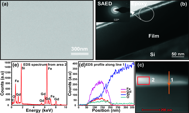
Fig. 2(a) and (b) exhibit the AFM and MFM images of the as-prepared film respectively, which indicate that the magnetic phase is free from topographic influences. MFM reveals elongated, periodic stripe domain pattern with high magnetic phase contrast. The domains are essentially the self organization of magnetization into alternating up-down magnetized areas with bright-dark contrasts. They are formed due to the competition between the exchange and anisotropy energies which favor a single domain state with magnetization perpendicular to the film plane, with long ranged demagnetizing field that favors the creation of in-plane (IP) domain walls by breaking the system into multi-domain state. The domain periodicity has been calculated from the 2D isotropic power spectral density (PSD) profile as in Fig. 2(c), estimated from the Fourier transform of the MFM image. This allows us to obtain the domain periodicity (twice the domain size) and their relative weight BMR_PRB_2007 . The peak of the PSD curve points out the wavelength of the most predominant feature in the image BLW_APL_2011 . The PSD is fitted with a Lorentzian to point out the mean value and standard deviation which account for the domain periodicity and the associated error bar respectively. The domain size turned out to be around 122 () nm by inverting the frequency of the 1st order peak. The presence of higher order peak signifies the long range correlation of the domains. Similar kind of domains in as-prepared Gd-Fe films has also been reported MPT_PRB_2006 . But, the magnetic properties are sensitive to the processing conditions BCR_TSF_2015 ; UCB_JMMM_2016 such as deposition temperature, pressure, time and internal stress as well.
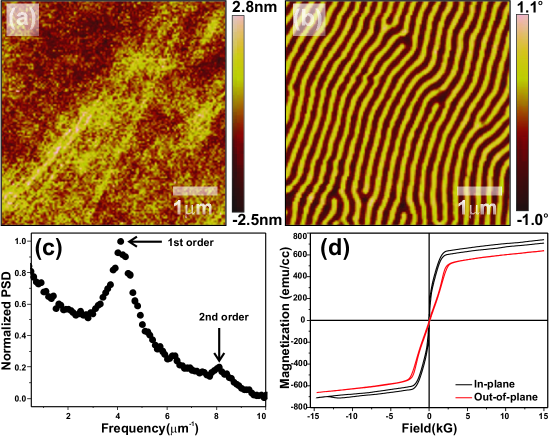
We have reported the evolution of meandering stripe domains in Gd-Fe thin films and the enhancement of perpendicular contrast as a function of film thickness by means of MFM and micromagetic simulation TAM_AIP_2017 . This kind of sub-200 nm sized domains are usually the signature of the development of weak PMA in thin films and results in a slanted hysteresis loop with almost zero remanence when measured along the out-of-plane (OOP) direction, as shown in Fig. 2(d). Similar feature of domains and hysteresis loop have also been reported for Co/Pt multilayer TAM_JMMM_2016 ; TAM_AIP_2016 and also in Gd-Fe thin films KML_JAP_2005 , where the presence of PMA has been claimed for all the cases. While the coercivity for the IP (51 Gauss) and OOP (43 Gauss) loops are comparable, the remanence is more for the IP loop as observed from Fig. 2(d).
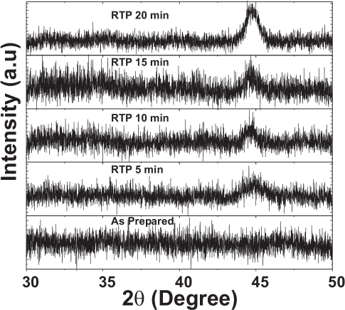
As our interest involves tailoring magnetic domains in Gd-Fe thin films, so we have performed RTP at for different time intervals viz. 5, 10, 15 and 20 min which results in a global change in material properties, unlike local modifications by laser LMV_SCI_14 ; TAM_JMMM_2016 or focused ion beam irradiation MMK_PRB_2012 ; KML_JAP_2005 or recent trend of voltage controlled magnetism SCL_PMC_2017 . While the as-prepared film shows amorphous nature, RTP induces crystallinity in the films, degree of which increases upon increasing processing time, as observed from the GIXRD data, shown in Fig. 3. The appearance of the peak at corresponds to the highest intensity peak of Fe from (110) plane (JCPDS card number: 00-006-0696). This designates the nucleation of crystalline Fe over the amorphous Gd-Fe matrix.
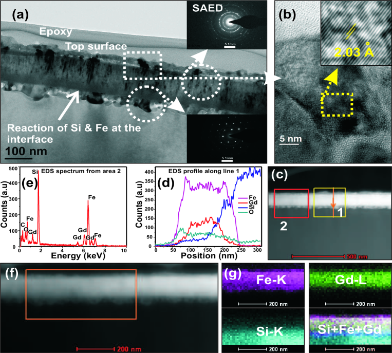
Further, this has been verified by XTEM images, performed on the film after RTP for 20 min (Fig. 4(a)) where the crystallinity is maximum. A clear indication about the presence of Fe near the top and bottom surface has been evidenced from the EDS line profile (Fig. 4(d)) of the cross-sectional HAADF-STEM image in Fig. 4(c). The composition is estimated to be along the depth. The top surface shows formation of nm-sized Fe crystallite, which is evident from the SAED pattern (inset of Fig. 4(a)). The d-spacings calculated from the diameter of the rings match with the reflections of Fe phase. The presence of spots confirms that the Fe nanocrystals are distributed over the amorphous phase of Gd-Fe. Furthermore, one of the crystalline Fe particles at the top surface has been shown in the high resolution TEM (HRTEM) image of Fig. 4(b). The lattice spacing is estimated to be 2.03 Å from the inverse Fourier filtered transform (IFFT) image derived from the area under the yellow dotted box in the HRTEM image and shown as the inset of Fig. 4(b). The value of the lattice spacing matches with (110) inter planar spacing of Fe as per the mentioned JCPDS file. Similar observation of the crystallization of FeCo alloy over amorphous TbFeCo matrix has been reported UBC_JAC_2016 . On top of that, elemental mapping (shown in Fig. 4(g))has been performed using HAADF-STEM-EDS technique along the area shown in Fig. 4(f). This verifies the presence of Fe and Gd over the considered area.
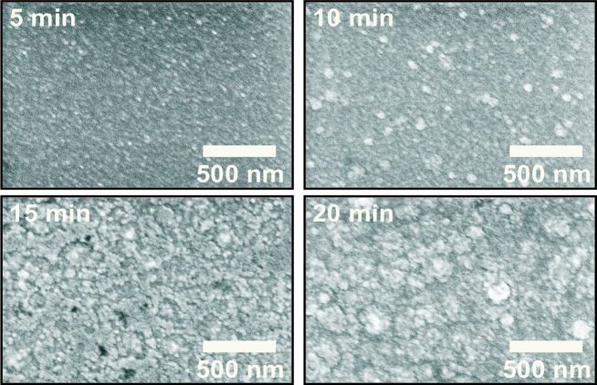
While the as-prepared film shows a feature-less smooth surface (Fig. 1(a)), the presence of island-like granular microstructure has been evidenced in the FESEM surface micrographs, as shown in Fig. 5. It can be qualitatively observed that the grains are randomly distributed over the surface and the grain size increases with the increase in RTP time. At 20 min RTP time, the size becomes maximum with highest irregularity in the distribution. The measurement of the overall composition by EDS showed a very little increment of the rare-earth metal upon increasing the RTP time and this is listed in Table 1.
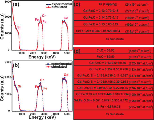
Further, the depth-resolved composition analysis has been carried out with RBS technique. The experimental and the simulated RBS spectra along with the simulation model have been shown in Fig. 6. The overall composition for the as-prepared film has been estimated to be , from the area under the experimental curve in Fig. 6(a). This is in well agreement with the EDS data. The best-fitted model of the experimental data for the as-deposited film has been shown in Fig. 6(c), which shows the inhomogeneous distribution of Gd and Fe across the cross-section of the film. The total thickness of the film, estimated from RBS also matches within the error bar of around 10% with respect to the thickness, recorded by the quartz crystal monitor. Now, the complexity arises after performing RTP. The experimental curve in Fig. 6(b) shows the RBS spectra for the film with processing time of 10 min. Calculation of the area under the curve unfurls that the overall composition remains almost unchanged after RTP, which has also been evident from the EDS data, recorded in table 1. The real picture of the depth-resolved composition variation can be understood from the best-fitted model, shown in Fig. 6(d). The integrity of Cr capping layer is commendable as it does not show any diffusion even after RTP. The most important feature is the nucleation of Fe, predominantly taking place near the top surface, elucidated from the RBS study. This is also in concurrence with the XTEM results, shown in Fig. 4(a). The reason behind the nucleation of Fe below the Cr layer could be probably due to the fact that Cr acts as nucleation center for the formation of Fe nano-crystal. This can be attributed to the closeness of the crystal structure and lattice parameter of Fe and Cr in comparison with Gd-Fe and Fe. On the other hand, the diffusion of Si has been evident near to the film-substrate interface which increases the probability for the formation of stable iron-silicide alloy at the interface. Moreover, the diffusion aided kinetics makes the reaction zone wider with the increase in RTP time UBC_JAC_2016 . Thus, the nucleation of Fe near the top surface and the formation of wider reaction zone at the film substrate interface results in the ingression of Gd and hence the presence of amorphous Gd-Fe alloy has been evidenced only in few intermediate layers. The results of RBS experiments are found to be in good agreement with the XTEM results (Fig. 4), where we get an extra information about the crystallization of Fe.
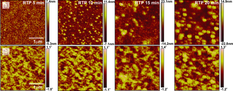
To probe the topography microscopically with higher resolution, AFM measurement has been carried out for all the films and are shown in the series of Fig. 7(a). Similar findings of increasing nano-crystalline grain growth has also been noticed with increasing RTP time. To get quantitative information from the AFM images, root mean square roughness (), grain diameter and the most probable threshold height () of the topographic features have been estimated and mentioned in Table 1. It has been observed that the increases monotonically with RTP time and reaches almost 4.25 times when RTP is performed for 20 min compared to that for the duration of 5 min. Due to the increasing RTP time, the crystalline grain diameter increases, but the size distribution gets broader (as the error is very high) for 20 min sample. This can be attributed to the increase in non-uniformity in the distribution of the crystallites over the film surface which has also been qualitatively understood from the FESEM images (Fig. 5). From the point of view of scanning probe microscopy, is an important criterion which designates the average height of the topographic feature with respect to the maximum height in the depth histogram analysis. The turns out to be maximum for the film with processing time of 15 min and again drops down for the film processed for 20 min. Comparatively higher value of the full width half maxima (FWHM) essentially proves again the non-uniform growth of the crystallites for the films with maximum processing time.
| RTP Time | Composition | Grain size ( error) | ( FWHM) | |
|---|---|---|---|---|
| (min) | (atomic %) | (nm) | (nm) | (nm) |
| 5 min | 2.0 | 140.4 (21.6) | 21.3 (3.2) | |
| 10 min | 2.5 | 138.4 (34.3) | 43.3 (3.4) | |
| 15 min | 4.8 | 173.5 (74.4) | 107.2 (7.2) | |
| 20 min | 8.3 | 289.0 (205.8) | 49.9 (15.1) |
Magnetic microstructure of the films has been imaged with MFM using a magnetized tip with a tip lift height of 50 nm from the film surface and the images are shown in Fig. 7(b). The area of scanning for the AFM and MFM images are same which helps to correlate the magnetic microstructure with the topographic feature. While the as-prepared film displays elongated stripe domains (Fig. 2(b)), the film with processing time of 5 min does not show any identifiable domain pattern. Two different magnetic contrasts appear in the form of irregular patches which essentially means that the PMA of the sample gets weaker and the formation of stripe domains is no longer energetically favorable. This may take place due to the modification of magnetic anisotropy after the RTP treatment. Hence, the magnetic phase contrast is expected to be weaker for the films with higher RTP time. We are unable to visualize this from the MFM images because the topographic features dominate over the magnetic phase. Starting from the sample with RTP time of 10 min, the of the crystallites (Table 1) becomes comparable to the lift height of the MFM tip. As a result, short ranged Van der Waals force wins over the long ranged magnetic force and topography dominated mixed phase is obtained. MFM has also been performed with higher lift heights (not shown here), but the weaker magnetic signal with strong topography results in noise in the images.
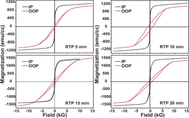
Fig. 8 represents the hysteresis loops for the films after RTP, measured along the IP and OOP geometry. The extracted magnetic properties are summarized in Table 2. It can be observed that the remanence and saturation magnetization () shows increasing trend with increasing RTP time for both the IP and OOP mode. But the specific value of the IP remanence is much greater than that in OOP mode. The increase in squareness (ratio of remanence to saturation magnetization) for the IP loops with RTP time suggests that RTP favors the magnetization to lie in the plane of the film surface, unlike in the case of the as-prepared film. Umadevi et al. UBC_JAC_2016 calculated the tilt angle of hard Tb-Fe-Co with increasing annealing time by using a formula mentioned in the reference CMF_JPD_2013 employing cosine inverse of the ratio of the remanent magnetization for the film after RTP to that of the as-prepared film. This calculation may show some meaningful result for the case of materials with strong PMA as in the case of Tb-Fe-Co, where the as-prepared film shows almost square hysteresis loop. Gd-Fe with comparably weak PMA, the way of calculation of tilt angle by similar method does not hold good. We need to understand the anisotropy modification in terms of increase in IP remanence and squareness compared to the OOP mode. On top of that, the OOP saturation field is almost three times the IP saturation field, which indicates that the IP direction becomes the preferential orientation of magnetization after RTP.
| RTP Time | IP (OOP) | IP (OOP) | IP (OOP) | IP (OOP) |
|---|---|---|---|---|
| (min) | (emu/cc) | (Gauss) | (emu/cc) | (Gauss) |
| 5 | 462 (70) | 97 (118) | 1007 (862) | 2138 (6585) |
| 10 | 559 (171) | 92 (938) | 1138 (1002) | 3283 (7445) |
| 15 | 579 (89) | 152 (474) | 1260 (1404) | 3292 (9988) |
| 20 | 562 (102) | 146 (609) | 1414 (1293) | 3345 (10020) |
It is well known that, the magnetic moment of Fe decreases when alloyed with rare-earth materials because of the crystal field effect. It has been reported that the magnetic moment of Fe in is estimated to be around (by Mössbauer studies), whereas the magnetic moment of free Fe is AMM_HI_2008 . Thus the nucleation of free Fe makes the of the processed films higher in comparison to the as-prepared film. Now, and effective anisotropy are related as:
| (1) |
where is the uniaxial anisotropy and is the magnetic permeability in free space. Hence, it is clear from the equation that increase in makes the effective perpendicular anisotropy lower. On top of that, Fe shows only in-plane anisotropy except for the case of controlled monolayer growth. Thus the observed magnetization behavior can be attributed to the Fe crystallization in the amorphous Gd-Fe matrix, which is responsible for the SRT from OOP to IP direction after RTP. However, the coercivity value is observed to be more in the OOP mode and varies somewhat randomly which can be corroborated to the increase in pinning sites along vertical direction due to the increased of the nano-crystallites.
In the light of the magnetic microstructure and magnetization measurements, it is evident that the magnetic anisotropy is getting modified due to RTP. But the experimental limitation hindered us to image the magnetic domain structure independently, without topographic influence. This has been complemented by 3D micromagnetic simulation, which directly shows the variation of magnetic domains as a function of anisotropy value as well as its IP tilt along the plane. The simulations of magnetic domains are carried out by OOMMF software OOMMF which performs the minimization of the total magnetic energy of the system, starting from a random state with uniform vertical () magnetization. The input parameters used for the simulations have been taken from literature MPT_PRB_2006 which include = , = and the exchange stiffness constant () = . The volume of each cell is taken to be , which is smaller than the exchange length () of the material. The effect of finite temperature has not been considered in the simulations.
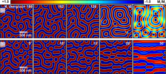
The first image of Fig. 9(a) shows the domain structure ( component of the magnetization vector) for a 100 nm thick Gd-Fe film, specified by the aforementioned input parameters. The two different contrasts (red and blue) in the image represent oppositely magnetized alternating up-down domains having magnetization parallel or anti-parallel to the surface normal. The total area of simulation () is much greater than the characteristic feature size of the domains, so the effect of truncation can be neglected. The domain in the first image of Fig. 9(a) shows a perfect demagnetized state with connected stripes and that can be considered to be comparable to the domain pattern for the as-prepared film as shown in Fig. 2(b). Line scans over the different areas of the domains indicate the average domain size to be around 107 ( 5) nm, which is comparable to the domain size obtained from the experiment. On top of that, the domain wall width ( component) turned out to be 26 ( 2) nm which matches very close to the theoretical value of 28 nm (). In order to study the effect of anisotropy in OOP to IP transition of the magnetization, we have systematically decreased the anisotropy value at an interval of 10% of the original value, mentioned earlier. The variation of domain size and domain wall width as a function of anisotropy value has been depicted in Fig. 10(a).
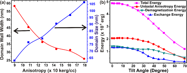
The simulated domain size decreases with decreasing the anisotropy and simultaneously the domain wall width increases. Finally, at (50% less compared to the original ), IP components come into the picture and as a result of that the elongated stripe pattern tries to shrink to a closed circular-like domains to minimize the magnetostatic energy. The comparable values of domain size and domain wall width at the same anisotropy value (Fig. 10(a)) also signifies a strong competition between the IP and OOP components of the magnetization. Similar observations on domain pattern were also reported for Co/Pt multilayer in response to ultrafast laser pulse and was also verified with micromagnetic simulations TAM_JMMM_2016 . The series of images in Fig. 9(b) shows the effect of anisotropy tilt along the plane. The first image in Fig. 9(b) series shows the domain configuration at tilt angle with respect to the fundamental one, shown in the first image of Fig. 9(a). With increasing tilt angle, the domain structure is getting modified and the random stripe domain pattern is converted to irregular discrete bubbles and patches with a preferential orientation along the longitudinal direction. This effect is very clear from the domain image with tilt angle of and more. Moreover, the contrast variation in the normalized images confirms the reduction in PMA and the resulting anisotropy does not energetically favor the formation of elongated periodic stripe domains which has also been evidenced from the experimental results. Recently we have reported a systematic transformation of magnetic domains from a meandering stripe state to elongated stripes with preferred orientation which further gets converted to magnetic patches (no-stripe state) with the increase in RTP temperature TAM_JMMM_2018 . While the irregular domain pattern with different color contrast hinders to estimate the domain size properly, the energetics of the system (Fig. 10(b)) clearly throw light towards the micromagnetic phenomena. The monotonic decrease in total energy of the system is followed by the decrease in other magnetic energies, namely uniaxial anisotropy energy (), exchange energy () and demagnetization energy () with increasing tilt angle. But the maximum variation of is calculated to be 75% whereas the other two energies show a negligible variation up to the tilt angle of . This may be considered as the threshold tilt angle in this material system to offer a SRT after which IP component of magnetization becomes dominant. As a result, and drops down to 84% and 62% respectively. Thus, our simulation results correlate the effect of magnetization tilt in magnetic microstructure as well as the energetics of the system.
IV Conclusion
Detailed study on structure, microstructure and magnetic properties have been performed on e-beam evaporated 100 nm Gd-Fe films, subjected to RTP for different time intervals. The as-deposited films are amorphous and display elongated stripe domains with higher magnetic phase contrast which symbolizes the development of PMA in the material. RTP treatment at for different time intervals induces the nucleation of Fe nanocrystals over the amorphous Gd-Fe matrix. The detailed structural study by XTEM reveals the presence of nanocrystalline Fe on the top surface and diffusion of Si at the film-substrate interface, quantification of which has been provided by RBS. FESEM surface micrographs and AFM show the irregular distribution of island-like grains on the surface, characteristic size of which increases with increasing RTP time. The magnetization studies explained that the films underwent a SRT with magnetization lying in the plane of the film surface upon different time interval of RTP, which could be probably due to the crystallization of Fe that gives an IP tilt to the magnetic moment. Special thrust has been given to understand the magnetic microstructure with the increase in RTP time. The decrease in magnetic contrast and simultaneous growth of topographic feature limit us to get a topography free magnetic contrast by MFM. To unravel the modification of domain structure, 3D micromagnetic simulations have been carried out which successfully explain the change in the domain pattern, their size, orientation and micromagnetic energetics of the system under the modification of anisotropy value and its direction.
Acknowledgment
The complete work has been carried out under the scope of the project DMRL/O/CARS-17, issued by DRDO, India.
References
- (1) T. Mizoguchi, G. S. Cargill, Magnetic anisotropy from dipolar interactions in amorphous ferrimagnetic alloys, J. Appl. Phys. 50 (1979) 3570.
- (2) R. E. Camley, Surface spin reorientation in thin Gd films on Fe in an applied magnetic field, Phys. Rev. B 35 (7) (1987) 3608.
- (3) R. E. Camley, D. R. Tilley, Phase transitions in magnetic superlattices, Phys. Rev. B 37 (7) (1988) 3413.
- (4) R. E. Camley, Properties of magnetic superlattices with antiferromagnetic interfacial coupling: magnetization, susceptibility, and compensation points, Phys. Rev. B 39 (16) (1989) 12316.
- (5) H. Fu, M. Mansuripur, P. Meystre, Generic source of perpendicular magnetic anisotropy in amorphous rare-earth-transition-metal films, Phys. Rev. Lett. 66 (8) (1991) 1086.
- (6) R. J. Gambino, J. J. Cuomo, Selective resputtering induced anisotropy in amorphous films, J. Vac. Sci. Tech. 15 (1978) 296.
- (7) W. H. Meiklejohn, Magnetooptics: a thermomagnetic recording technology, Proc. IEEE 74 (11), (1986) 1570.
- (8) P. Hansen, C. Clausen, G. Much, M. Rosenkranz, K. Witter, Magnetic and magneto-optical properties of rare-earth transition-metal alloys containing Gd, Tb, Fe, Co, J. Appl. Phys. 66 (1989) 756.
- (9) T. Eimüller, R. Kalchgruber, P. Fischer, G. Schütz, P. Guttmann, G. Schmahl, M. Köhler, K. Prügl, M. Scholz, F. Bammes, G. Bayreuther, Quantitative imaging of magnetization reversal in FeGd multilayers by magnetic transmission x-ray microscopy, J. Appl. Phys. 87 (9) (2000) 6478.
- (10) J. Miguel, J. F. Peters, O. M. Toulemonde, S. S. Dhesi, N. B. Brookes, J. B. Goedkoop, X-ray resonant magnetic scattering study of magnetic stripe domains in -GdFe thin films, Phys. Rev. B 74 (2006) 094437.
- (11) Miguel, J. Ph.D thesis, “Static and dynamic X-ray resonant magnetic scattering studies on magnetic domains”, University of Amsterdam (2005), https://iop.fnwi.uva.nl/cmp//scientific_output/phd_theses.html.
- (12) S. Mangin, F. Montaigne, A. Schuhl, Interface domain wall and exchange bias phenomena in ferrimagnetic/ferrimagnetic bilayers, Phys. Rev. B 68 (2003) 140404(R).
- (13) S. Mangin, T. Hauet, Y. Henry, F. Montaigne, E. E. Fullerton, Influence of lateral domains and interface domain walls on exchange-bias phenomena in GdFe / TbFe bilayers, Phys. Rev. B 74 (2006) 024414.
- (14) I. Radu, C. Stamm, A. Eschenlohr, F. Radu, R. Abrudan, K. Vahaplar, T. Kachel, N. Pontius, R. Mitzner, K. Holldack, A. Föhlisch, T. A. Ostler, J. H. Mentink, R. F. L. Evans, R. W. Chantrell, A. Sukamoto, A. Itoh, A. Kirilyuk, A. V. Kimel, T. Raising, Ultrafast and distinct spin dynamics in magnetic alloys, Spin 5(3) (2015) 1550004.
- (15) A. Tripathi, J. Mohanty, S. H. Dietze, O. G. Shpyrko, E. Shipton, E. E. Fullerton, S. S. Kim, I. Mcnulty, Dichroic coherent diffractive imaging, Proc. Nat. Acad. Sci. 108 (33) (2011) 13393.
- (16) S. Konings, J. Miguel, J. Luigjes, H. Schlatter, H. Luigjes, J. Goedkoop, V. Gadgil, Lock in of magnetic stripe domains to pinning lattices produced by focused ion-beam patterning, J. Appl. Phys. 98 (2005) 054306.
- (17) K. Umadevi, S. Bysakh, J. Arout Chelvane, S. V. Kamat, V. Jayalakshmi, Tailoring magnetic anisotropy in Tb-Fe-Co thin films by rapid thermal annealing, J. Alloy. Comp. 663 (2016) 430.
- (18) V. Baltz, A. Marty, B. Rodmacq, B. Dieny, Magnetic domain replication in interacting bilayers with out-of-plane anisotropy: application to Co/Pt multilayers, Phys. Rev. B 75 (2007) 014406.
- (19) S. R. Bakaul, W. Lin, T. Wu, Evolution of magnetic bubble domains in manganite films, Appl. Phys. Lett. 99 (2011) 042503.
- (20) H. Basumatary, J. Arout Chelvane, D. V. Sridhar Rao, S. V. Kamat, R. Ranjan, Effect of sputtering parameters on the structure, microstructure and magnetic properties of Tb-Fe films, Thin Sol. Film 583 (2015) 1.
- (21) K. Umadevi, J. Arout Chelvane, H. Basumatary, M. Ramudu, S. V. Kamat, V. Jayalakshmi, Role of processing parameters on the morphology and magnetic properties of Tb-Fe-Co thin films, J. Magn. Magn. Mater. 418 (2016) 163.
- (22) A. Talapatra, J. Arout Chelvane, J. Mohanty, Microscopic understanding of domain formation in Gd-Fe thin films, AIP Conf. Proc. 1832 (2017) 130044.
- (23) A. Talapatra, J. Mohanty, Laser induced local modification of magnetic domain in Co/Pt multilayer, J. Magn. Magn. Mater. 418 (2016) 224.
- (24) A. Talapatra, J. Mohanty, Magnetic domain and domain wall in Co/Pt multilayer, AIP Conf. Proc. 1731 (2016) 130027.
- (25) C-H. Lambert, S. Mangin, B. S. D. Ch. S. Varaprasad, Y. K. Takahashi, M. Hehn, M. Cinchetti, G. Malinowski, K. Hono, Y. Fainman, M. Aeschlimann, E. E. Fullerton, All-optical control of ferromagnetic thin films and nanostructures, Science 345 (2014) 1337.
- (26) A. Maziewski, P. Mazalski, Z. Kurant, M. O. Liedke, J. McCord, J. Fassbender, J. Ferré, A. Mougin, A. Wawro, L. T. Baczewski, A. Rogalev, F. Wilhelm, T. Gemming, Tailoring of magnetism in Co/Pt/Co ultrathin films by ion irradiation, Phys. Rev. B 85 (2012) 054427.
- (27) C. Song, B. Cui, F. Li, X. Zhou, F. Pan, Recent progress in voltage control of magnetism: materials, mechanisms, and performance, Prog. Mater. Sci. 87 (2017) 33.
- (28) S. Chung, S. M. Mohseni, V. Fallahi, T. N. Anh Nguyen, N. Benatmane, R. K. Dumas, J. Åkerman, Tunable spin configuration in [Co/Ni]-NiFe spring magnets, J. Phys. D: Appl. Phys. 46 (2013) 125004.
- (29) J. Arout Chelvane, G. Markandeyulu, M. Manivel Raja, Magnetic properties and Mössbauer studies in , Hyperfine Interact. 184 (2008) 27.
- (30) M. Donahue, D. G. Porter, OOMMF user’s guide, version 1.0, Intergency Report NISTIR 6376, Nat. Inst. of Standard and Tech. Gaithersburg, MD, http://math.nist.gov/oommf.
- (31) A. Talapatra, J. Arout Chelvane, J. Mohanty, Tuning magnetic microstructure in Gd-Fe thin films: experiment and simulation, J. Magn. Magn. Mater. 448 (2018) 360.