A photon ratchet route to high-efficiency hybrid halide perovskite intermediate band solar cells
Abstract
The spin-split indirect bandgap in hybrid-halide perovskites provides a momentum-space realisation of a photon-ratchet intermediate band. Excited electrons thermalise to recombination-protected Rashba pockets offset in momentum space, building up the charge density to have sufficient flux to the higher lying conduction band. This effect could be used to form an intrinsic intermediate band solar cell with efficiencies beyond the Shockley-Queisser limit if a selective low-electron affinity contact can be made to the higher conduction state. This concept is supported by analysis of the many-body electronic structure. Production of above-bandgap voltages under illumination would affirm the physical mechanism proposed here.
The Intermediate Band Solar Cell (IBSC)Luque and Martí (1997); Okada et al. (2015) is a photovoltaic device architecture that offers the potential to significantly exceed the Shockley-Queisser (SQ) power conversion efficiency limit. By introducing an additional intermediate band, there are three excitation processes at different wavelengths that subdivide the solar spectrum. A working realisation has so-far been prevented by the fact that any state introduced within the gap also provides a route for recombination. IBSC cells considered to date create an intermediate band by doping the crystal with defects, or by creating a quantum-dot superstructure. The high emission rate competes strongly with the absorption to the conduction band.
A necessary condition for an IBSC is that independent quasi-Fermi levels can be maintained in each of the three bands. This requires that electrons cannot transport between the bands, either directly (phonon mediated) or via a continuum of electronic states in the contacts.
If the device is to exceed the SQ limit, the charge density in the intermediate state must build sufficiently for balanced absorption to the conduction band. A long-lived intermediate state has been identified as a key requirement for a working IBSC. This is challenging with a single intermediate band, since spontaneous emission back down to the valence band also increases with the occupation of the intermediate band. Recently, the photon ratchet mechanism was proposedYoshida et al. (2012), where the photoexcited intermediate band thermalises into another state, with reduced recombination rate to the ground state. This process significantly increases the lifetime of the intermediate state and provides a promising route for realising high-efficiency IBSC.
In this Letter, we propose that the spin-split indirect-gapAzarhoosh et al. (2016) in methylammonium lead halide perovskite (\ceCH3NH3PbI3) forms an intermediate band. A photon-ratchet effect is provided by carriers excited into this band, relaxing in momentum space to the Rashba pocket (see Figure 1). This mechanism is intrinsically present in the bulk material.
Electron-hole recombination to the valence band (VB) from both the intermediate band (IB) and conduction band (CB) is reduced by the slightly indirect gap originating from the mutually-orthogonal Rashba extremal points. Both the middle bands and the conduction bands are spin split due to spin-orbit coupling, but along different axes; thus none of the bands have extremal points at the same in momentum space. A quasi-equilibrium distribution of electrons give rise to a low joint density-of-states for vertical transitions. We invoked a similar mechanismAzarhoosh et al. (2016) for conduction to valence band transitions in order to explain and quantify the long charge-generated carrier recombination times in lead halide perovskites with standard device architectures.
The excitation from the VB to IB is at 1.6 eV, while the direct VB to CB excitation at 3.1 eV.Leguy et al. (2016) These states are optically bright. The photon ratchet from the IB to the CB would operate at 1.6 eV. These energies are not well matched to subdivide the solar spectrum, but they are accessible in the laboratory. To exceed the SQ limit, a smaller bandgap material is required. However, we propose lead halide perovskites as a well understood test system in which the physics can be studied, to leverage expertise in making high-quality materials and devices. A working IBSC should also be an upconverter when operating at open circuit (or equivalently, with no contacts). This will require a pure material where non-radiative recombination pathways to be sufficiently suppressed to observe light output.
The higher lying conduction band provides a high dispersion (low effective mass) band from which to extract the charge carriers. The only change in device architecture required is a low work-function electron-accepting contact (such as Ba, Ca, LiF, or fulleroid adduct), to selectively collect from the higher energy CB. With suitable contacts, the material should thus be able to generate an anomalous photovoltage, above circa. ) when pumped with incident light of 1.6 eV.
Qualitative model: There are two necessary conditions for a working IBSC: (i) the CB and IB should develop independent quasi-Fermi levels; (ii) the CB must be electrically contacted independent of the IB. We can assess whether these conditions are achievable by inspecting the electronic band structure.
Band structures are usually presented as cross-sections of the Brillouin zone, with the path chosen to follow an irreducible representation of the underlying crystal symmetry. From the Bloch theorem, these high symmetry lines form the extrema and turning points in the electronic structure, and so fully characterise the band functions. In hybrid halide perovskites, the presence of a molecule (and large dynamical flexing of the octahedral cage) breaks the local symmetry of the underlying pseudo-cubic lattice. Practically, the spin-orbit coupling (due to atoms with large nuclear charges) interacting with local crystal fields moves band extrema to off-symmetry locations. Amongst other effects, this results in the splitting of the lower conduction-band to give a spin-split indirect-gap. To guarantee that we are exploring all possible routes for recombination and thermalisation, we must integrate over the Brillouin Zone. By considering the reciprocal-space resolved difference in energy eigenstates, we can demonstrate whether the two conditions for an IBSC are met.
We use the QSGW electronic structure method as implemented in the Questaal codesQue , improving on our prior workBrivio et al. (2014) by using a larger and more converged basis on the same pseudo-cubic structure. It has been establishedChantis, van Schilfgaarde, and Kotani (2006); Krich and Halperin (2007) that QSGW yields very good Dresselhaus splitting in semiconductors, in contrast to the LDA. For convenience, the spin-orbit coupling was added only as a post-processing step: if it is included in the self energy the gap is reduced about 0.1 eVBrivio et al. (2014)). These codes allow for the calculation of a self-consistent self-energy on a regular k-point mesh, which can then be used for calculation at an arbitrary k point. This allows for sufficient finesse to locate and characterise the slightly off-symmetry extrema. Thus we consider this method to be of the highest quality available for broken-symmetry relativistic-ion semiconductors such as \ceCH3NH3PbI3.
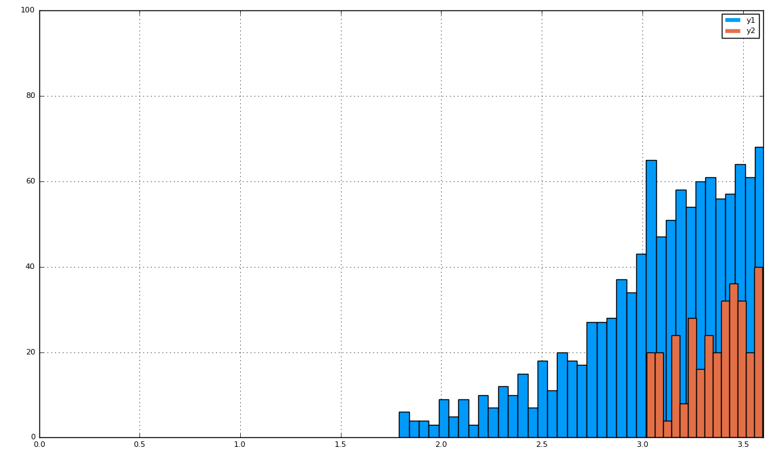
We find no connection between bands in an energy window around the photo excited charge carriers, but at very high energies above the Fermi level, the bands do come together. This suggests that distinct quasi-Fermi levels are experimentally realisable. A consideration of the joint densities of state indicate that both the VB to IB and VB to CB photoexcitation channels will be simultaneously operational (Figure 2).

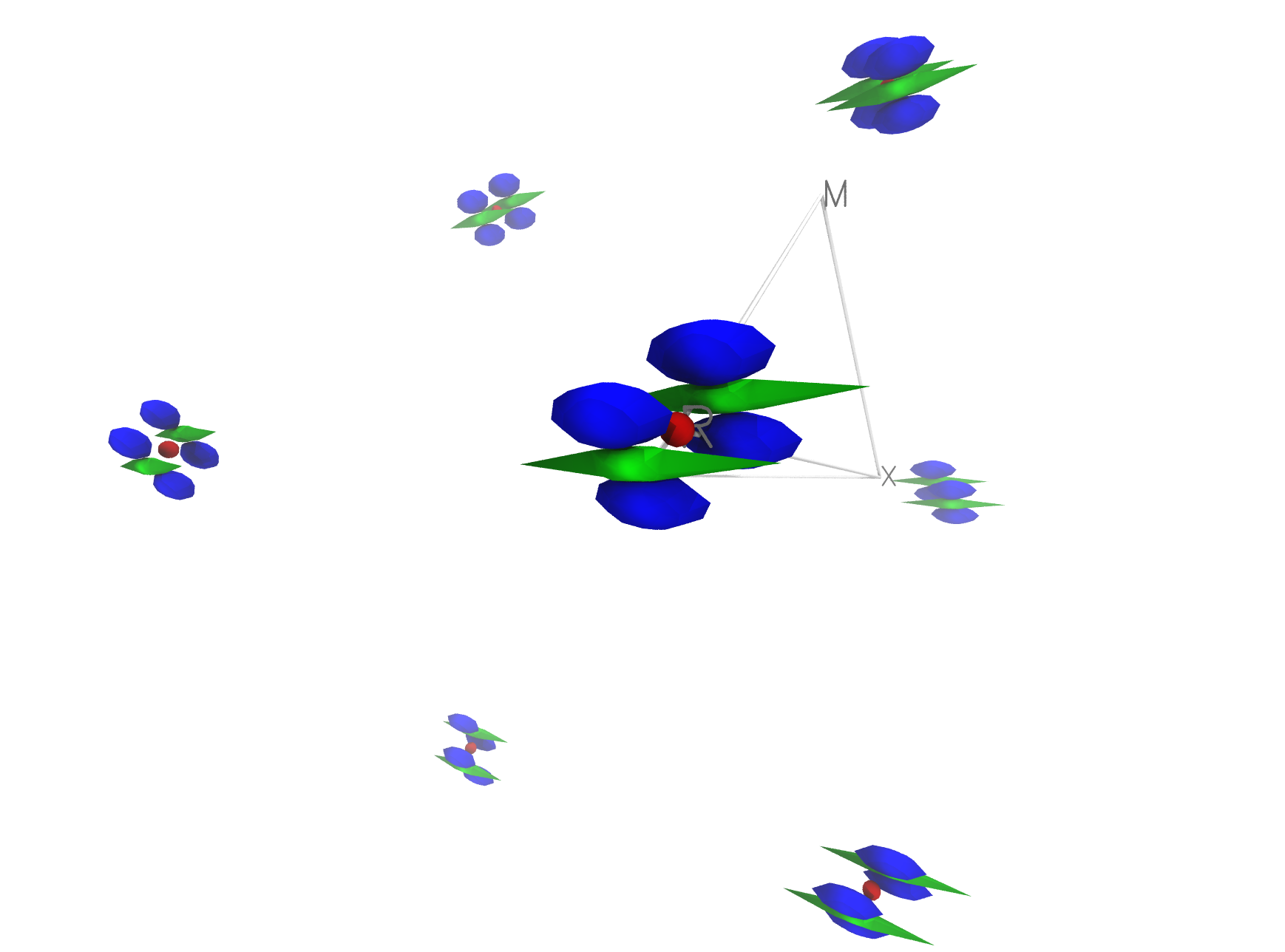
The band-edge electronic structure for hybrid perovskites is unique: there is a dispersive upper valence band (formed of I orbitals), an intermediate band (mainly hybridised Pb orbital), and the upper conduction band (two-fold degenerate, mainly hybridised Pb orbitals).
These extrema are centered around the high symmetry point in the Brillouin zone.
The spin-orbit coupling (due to large nuclear charge on Pb and I, and associated relativistic term in the Hamiltonian) interacts with the local crystal field to split the spin degeneracy, projecting differing spin electrons to antipodal locations around . This effect leads to the spin-split indirect-gap. As the orbital character is different for all three bands, we find that the reciprocal space projection is mutually orthogonal. Spin-split indirect-gaps exist between all VB, IB and CB.
| Band | |||||
|---|---|---|---|---|---|
| VB | 2 | ||||
| IB | 2 | ||||
| CB | 4 |
| Band | ||||
|---|---|---|---|---|
| VB | ||||
| IB | ||||
| CB |
In the equivalent circuit of an IBSC, the VB to IB and IB to CB transition are connected in series by the conservation of electron charge; forming equivalent circuit of a two-lead tandem solar cell. Therefore an efficient device requires the current flux between the two processes to be balanced. This depends on the details of the band structure, including the bandgap, density of states, and the strength of the optical transitions (transition matrix elements). The critical factor for hybrid perovskites, which is not present in tetrahedral semiconductors such as GaAs, is the reduced electron-hole recombination rates due to Rashba splitting. As discussed above, these will affect CB VB and IB VB transitions, due to a momentum offset between thermalised populations of electrons and holes. Our prior analysisAzarhoosh et al. (2016) has shown that the direct radiative recombination rate is reduced by a factor of 350X under one sun illumination. This will ensure significant steady state population of electrons in the IB under working conditions.
In summary, we have proposed a novel route to achieve intermediate band solar cells based on spin-split indirect-gap materials such as hybrid perovskites. According to the calculations presented herein, with suitable contacts \ceCH3NH3PbI3 should make a working device, with all transitions in the visible, and accessible in the laboratory. In order to quantitatively predict whether a device with efficiencies beyond the SQ limit is achievable will require more detailed device simulations that takes into account the unusual band physics, including the asymmetry in absorption and recombination between the three band system (VB, IB and CB).
Beyond \ceCH3NH3PbI3, in looking for spin-split materials to make high power conversion efficiency IBSC devices, we want to identify materials with a lower band-gap than the SQ matched 1.5 eV. Searches of novel materials for photovoltaics often discard such low-gap materials. An exciting prospect of using a bulk, band structure engineered, material for IBSC is the relatively low cost of making the devices, compared to engineering real-space heterojunctions.

Acknowledgement We thank Jenny Nelson and N. J. Ekins-Daukes (NED), for stimulating discussion. We acknowledge membership of the UK’s HPC Materials Chemistry Consortium, which is funded by EPSRC grant EP/F067496. J.M.F. is funded by EPSRC Grant EP/K016288/1, the KCL group acknowledges support from EPSRC Grant EP/M009602/1. A.W. acknowledges support from the Royal Society. The authors declare no competing financial interests.
References
- Luque and Martí (1997) A. Luque and A. Martí, Physical Review Letters 78, 5014 (1997).
- Okada et al. (2015) Y. Okada, N. J. Ekins-Daukes, T. Kita, R. Tamaki, M. Yoshida, A. Pusch, O. Hess, C. C. Phillips, D. J. Farrell, K. Yoshida, N. Ahsan, Y. Shoji, T. Sogabe, and J.-F. Guillemoles, Applied Physics Reviews 2, 021302 (2015).
- Yoshida et al. (2012) M. Yoshida, N. J. Ekins-Daukes, D. J. Farrell, and C. C. Phillips, Appl. Phys. Lett. 100, 263902 (2012).
- Azarhoosh et al. (2016) P. Azarhoosh, S. McKechnie, J. M. Frost, A. Walsh, and M. van Schilfgaarde, APL Mater. 4, 091501 (2016).
- Leguy et al. (2016) A. M. A. Leguy, P. Azarhoosh, M. I. Alonso, M. Campoy-Quiles, O. J. Weber, J. Yao, D. Bryant, M. T. Weller, J. Nelson, A. Walsh, M. van Schilfgaarde, and P. R. F. Barnes, Nanoscale 8, 6317 (2016).
- (6) “Questaal,” https://lordcephei.github.io/, accessed: 2016-11-22.
- Brivio et al. (2014) F. Brivio, K. T. Butler, A. Walsh, and M. van Schilfgaarde, Phys. Rev. B 89 (2014), 10.1103/physrevb.89.155204.
- Chantis, van Schilfgaarde, and Kotani (2006) A. N. Chantis, M. van Schilfgaarde, and T. Kotani, Phys. Rev. Lett. 96, 086405 (2006).
- Krich and Halperin (2007) J. J. Krich and B. I. Halperin, Phys. Rev. Lett. 98, 226802 (2007).