Fano lines in the reflection spectrum of directly coupled systems of waveguides and cavities: measurements, modeling and manipulation of the Fano asymmetry
Abstract
We measure and analyze reflection spectra of directly coupled systems of waveguides and cavities. The observed Fano lines offer insight in the reflection and coupling processes. Very different from side-coupled systems, the observed Fano line shape is not caused by the termini of the waveguide, but the coupling process between the measurement device fiber and the waveguide. Our experimental results and analytical model show that the Fano parameter that describes the Fano line shape is very sensitive to the coupling condition. A movement of the fiber well below the Rayleigh range can lead to a drastic change of the Fano line shape.
I Introduction
Photonic crystal (PhC) mitbook cavities are of tremendous interest for device applications due to their beneficial properties such as small mode volume and high quality factor () Kuramochi2006 ; Tanabe2007 ; Song2005 . Multiple-cavity systems are great platforms to study fundamental physics and build all-optical devices Yariv1999 ; Hafezi2013 ; Notomi2008 ; Xia2007 ; Hartmann2008 ; Yanik2004 . Thus, the characterization of multiple-cavity systems composed of photonic crystal cavities is of great importance. Reflection measurement is a typical way of characterizing resonant systems. From a reflection spectrum, the resonance width and frequency can be obtained. Depending on the structure of a system, resonances shown in a spectrum can be Lorentzian shape or Fano line shape Fano1961 .
The Fano line shape shows up when a narrow resonance interferes with a continuum. Depending how the continuum interacts with the resonance, a Fano line can show up various profiles Fano1961 ; Miroshnichenko2010 . In many cases, the sharp asymmetric Fano line shape is preferred to the Lorenztian shape. For example, for optical switching Fano resonances reduce the switching thresholds and give much larger switching contrast Yang2007 ; Nozaki2013 . Fano lines appear very often and are widely studied in side-coupled single and multi-cavity and waveguide systems. For side-coupled single cavity and waveguide systems, Fano lines can be created by adding extra scattering or reflecting elements in waveguides since transmission is open within the bandwidth of the waveguides Fan2002 ; Heuck2013 ; Yu2014 . For side-coupled multi-cavity and waveguide system, Fano line shapes show up naturally due to the direct and indirect cavity-cavity couplings even without extra scattering and reflecting elements lin2005 ; zhou2014 .
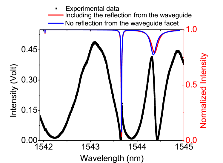
The situation is different in directly coupled single and multi-cavity and waveguide systems (Fig.1). In such systems transmission is only open at the cavity resonance, and indirect cavity-cavity couplings are absent. In case the light frequency is far off the resonance of the PhC cavity, light will be completely reflected, since the system is closed. Therefore, reflection of the facet of the PhC waveguide does not drastically change the line shape. Only in case the frequency of the incident light is close to the resonance of the PhC cavity, the reflection of the waveguide plays a role. In Fig. 2, we show the calculated spectra of direct-coupled multi-cavity and waveguide systems in two different cases, one with the consideration of the reflection of the waveguide, the other without taking into account of the reflection of the waveguide. In both cases, we see symmetric Lorentzian shapes. In contrast, we observe sharp asymmetric line shapes on top of Fabry-Pérot fringes in our experiments. Apparently, the observed strong asymmetric Fano line shape in a directly coupled systems can not be solely attributed to the termini of the waveguide.

The possibility to tune the asymmetry of the Fano line shape also arouses much interest. This tuning has been achieved by tuning the cavity resonances Fan2002 ; Xiao2009 ; Verhagen09 ; Frimmer2012 . For a given cavity, by deliberate design of the coupling to the continuum, different Fano line shapes can be obtained by fabricating different samples Chang2013 ; Yu2014 ; Zhang2016 . However, after the structure is fabricated, it is very difficult to change the Fano line shape without changing the frequency of the resonance because this requires to change the properties of the continuum or the broad resonances.
In this work, we experimentally and theoretically investigate Fano resonances in a multiple-cavity system directly coupled to a waveguide in a PhC membrane structure. We measure the Fano lines and manipulate their shape by tuning the resonances. We create an analytical model which uncovers the origin of the Fano line shape, and it accurately reproduces our experimental results. With the help of our model, we propose and experimentally demonstrate a way of directly manipulating the Fano lineshape without tuning the cavity resonances.
II Theoretical model
The schematic of the system we consider is shown in Fig. 3. We explicitly include the lensed fiber used to couple light into the waveguide. Light propagation in this system can be separated into three processes. The first process is the light coupling between the lensed fiber and the input waveguide. The second process is the light transport in the input waveguide. The last process is the light coupling between the waveguides and cavities. A correct description of the coupling process between the lensed fiber and the input waveguide is essential for the formation the Fabry-Pérot fringes in Fig. 2.
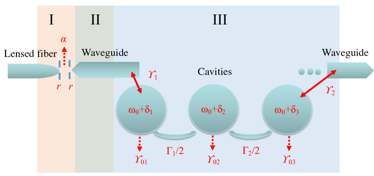
We use transfer matrices to model all these processes. The transfer matrix Hausbook ; Soukoulis connects the fields of forward and backward propagating waves from the left side to the right side,
| (1) |
Here is the forward (backward) propagating wave on the right side, is the forward (backward) propagating wave on the left side and M is the transfer matrix that links them. The matrices describe each process are discussed in the appendix.
III Experimental setup and reflection spectra
In Fig. 1 we show a representation of the sample. Our sample is a photonic crystal membrane structure made of InGaP alfredoapl2009 with a thickness of 180 nm. The lattice constant is nm, the radius of the holes is . There are two waveguides shown in the sample in Fig. 1. One is the input waveguide with the width of 1.1. The length of it is 219. The other one is the barrier waveguide, the width of it is . In the barrier waveguide, there are three mode-gap cavities Kuramochi2006 . They are created by shifting the holes around the barrier waveguide (Fig. 1). An output waveguide which is in line with the input waveguide is also in the structure. However, it is placed further away from the third cavity. A polarization maintaining lensed fiber (red cone in Fig. 1) with numerical aperture (NA) 0.55 is used to couple light from a tunable continuous wave (CW) infrared (IR) laser to the sample. A fiber circulator is used to connect the lensed fiber and laser. The third port of the fiber circulator is connected to a photodiode to measure the reflection spectra of the sample.
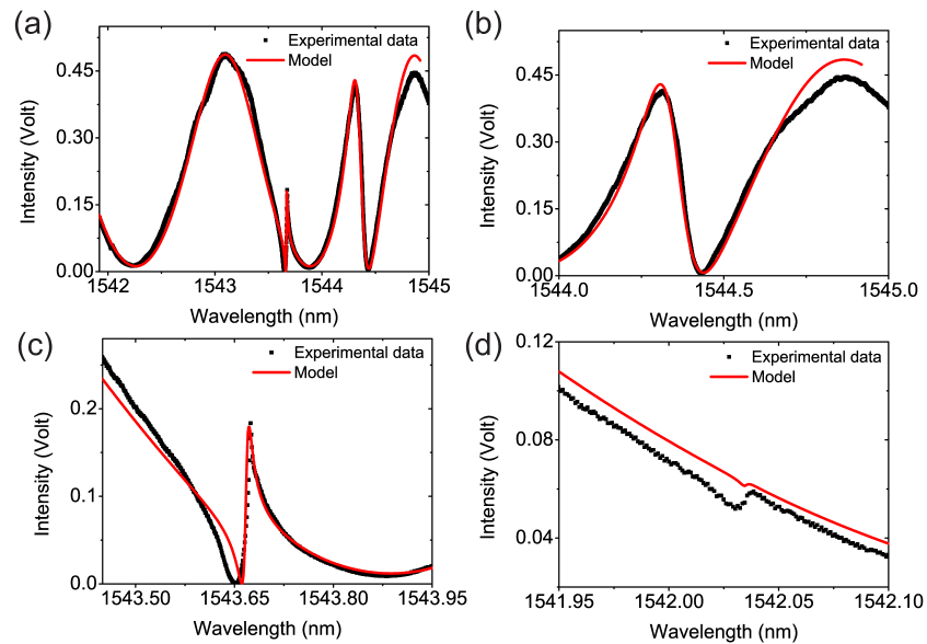
The reflection spectrum is shown in Fig. 4. In Fig. 4(a), we see that the cavity resonances form different lineshapes on top of Fabry-Pérot fringes. The first Fano resonance (Fig. 4(b)) is between 1544 nm and 1545 nm, and is a wide and deep valley with a slight asymmetry. The second Fano resonance is between 1543.5 nm and 1544 nm, it has a sharp asymmetric line shape. The peak intensity of this resonance is twice smaller than the maximum intensity of the background fringes. The third resonance (Fig. 4(c)) between 1541.95 nm and 1542.10 nm is less pronounced.
In order to cancel the disorder of the cavities Sokolov2017 , we use a CW diode laser (nm) to tune the frequencies of the cavities in the sample by laser induced heating Sokolov2015 . To control the first and third cavity simultaneously, two foci are projected on the surface of the sample by an objective with NA 0.4. These foci are generated with the help of a reflective spatial light modulator (SLM) in the pump path. A digital holographic phase pattern is written on the SLM for the generation of the foci Pasienski08 .
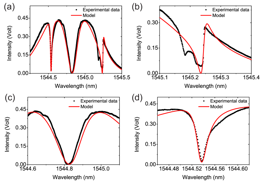
When the laser spots are focused on the cavities, their resonances are tuned to the red. Although there is no direct laser light on the second cavity, the resonance of cavity 2 also shifts due to heat diffusion. The reflection spectrum of the tuned device is shown in Fig. 5 Sokolov2017 . The power of the spots on cavity 1 and cavity 3 is 9 W and 108 W respectively. We see that in Fig. 5(a) the three resonances occur within 1 nm in the spectrum. One is with sharp asymmetric line shape. The other two have less asymmetric line shape and form two deep valleys in the spectrum. The modulation of the Fano dip shown in Fig. 6(b) is attributed to SLM noise.
IV Analysis of reflection spectra
The analysis of the reflection spectra is done by fitting experimental results with our model. We first fit the original spectrum, then the spectrum of the tuned device. The values of the parameters in our model are listed in Table 1.
| Parameter | Reference | Tuned |
| (nm) | ||
| (nm) | ||
| (nm) | ||
| (nm) | ||
| a and is 1544.790 nm. . The values of and have been obtained from our previous work Sokolov2017 . | ||
The fit of our model to the original spectrum is shown in Fig. 4. The fit agrees very well with our data for resonances 1, 2 and the background fringes. It accurately characterizes the period and visibility of the fringes. Meanwhile, it describes the line shapes, widths, heights of the peaks and depths of the trough for resonances 1 and 2. However, we cannot correctly reproduce the depth and width of resonance 3 at the same time. The probable cause for this is a direct coupling term between the waveguide and cavities 2 and 3, or a second neighboring coupling between the cavities. Such terms have been ignored in our model as they would lead to an excessive number of free parameters.
The fit of our model to the tuned reflection spectrum is shown in Fig. 5. We see that for all three resonances the fit agrees very well with experimental data. There are slight deviations on wings of the resonances between the fit and experimental data. These wings are mostly determined by the Fabry-Pérot fringes. To characterize them accurately, the accurate knowledge of the curvature of the PhC waveguide band is needed. In our model, we only use two parameters and to describe the band. This is an approximation only valid for a narrow frequency band. The values are obtained by fitting from the reference spectrum shown in Fig 4(a). Thus, the small deviation shown in the tuned spectrum which is in a different wavelength range is reasonable.
The fact that the fit from our model has an excellent agreement with the experiment shows that our model describes the physical process of the system accurately. It not only explains the physical origin of the observed Fano resonances but also provides the key parameters of the sample such as the intrinsic loss rates of the cavities. The fitting results show that the intrinsic factor is larger than . After we apply the tuning the frequency detuning between cavity 1 and 2 is reduced below their coupling rate, the same holds for cavities 2 and 3.
V Sensitivity of the Fano line shape
We can describe the lensed fiber, air gap, input waveguide and the cavities together as a special Fabry-Pérot cavity. If we ignore the reflection from the facet of the input waveguide, the first “mirror” of this Fabry-Pérot cavity is the tip of the lensed fiber, the second “mirror” of this cavity is the system of photonic crystal cavities. The length of the cavity is the total length of the air gap together with the input waveguide. The phase shift of a single round trip of this Fabry-Pérot cavity consists of two parts, the first is the phase shift from propagation and the second is the phase shift due to the reflection from the second “mirror”. The specialty of the second “mirror” is that it is very dispersive around the cavity frequencies. The Fano line shape is determined by the phase shift of the round trip. Therefore, we conclude that the Fano lineshape of the resonance can be tuned by changing the length of the air gap.
We perform an experiment to test this prediction on a new sample with the same parameters as our previous sample. Due to the inevitable disorder, the resonance positions of the cavities appear at different wavelengths. We measure reflection spectra with different sizes of the air gap. This was done by moving the sample step by step away from the lensed fiber with our precise translation stage.
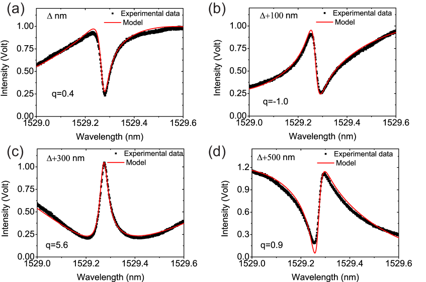
The measured reflection spectra are shown in Fig. 6. In Fig. 6(a), the reference spectrum is presented (the reference distance between the lensed fiber and sample is denoted by and is the distance where the coupling is optimized), and we see a Fano resonance is in the form of a dip with a bit asymmetry. After the reference measurement, we increase the length of the air gap with a step size of 100 nm. The spectra with air gap sizes nm, nm and nm are shown in Fig. 6(b), Fig. 6(c) and Fig. 6(d) respectively. In Fig. 6(b), we see a sharp asymmetric Fano resonance with a peak at short wavelength and a dip at a longer wavelength. In complete contrast to the reference spectrum, we see a peak with a slight asymmetry instead of a dip in Fig. 6(c). In Fig. 6(d), we again see a sharp asymmetric Fano resonance, however, it is almost a flipped version of Fig. 6(b). It has a dip at a short wavelength and peak at a longer wavelength. We also retrieve the q parameter that describes the asymmetry of Fano lines using the Fano line formula Miroshnichenko2010 . We also plot the fits from our analytical model. In the fits, all further parameters are kept the same for the results from Fig. 6(a) to Fig. 6(d) except the coupling loss, since it increases slightly as we increase the size of the air gap. The fits agree well with our experiment, which confirms that changing the air gap size causes the drastic change of the Fano line shape. The results shown in Fig. 6 confirm our prediction that the shape of a Fano resonance can be tuned by changing the size of the air gap between the sample and lensed fiber, and demonstrate that the origin of the Fano line shape is indeed the interference of the sharp resonances with the broad resonances defined by the reflection of the lensed fiber and coupling loss. The maximum distance we move the fiber to manipulate the Fano line shape is only 500 nm from the optimal coupling point. Since the Rayleigh range is 1.9 m, the coupling efficiency only experiences a very small change. On the contrary, the Fano line shape as we show in Fig. 6 experiences a drastic change.
VI Conclusion
In summary, Fano resonances in the reflection spectra of a direct-coupled waveguide-cavities system in a photonic crystal membrane structure have been experimentally and theoretically investigated. Our theoretical model has an excellent agreement with our experimental results and provides important information on the very low bare loss rate of the cavities. The origin of the Fano lineshape is the interference between the wave reflected from the lensed fiber and the wave reflected from the photonic crystal cavities. The path length difference between these waves is a round trip of the air gap size and the input waveguide. We propose and experimentally show that the Fano asymmetric parameter can be tuned drastically by only changing the air gap size between the sample and the fiber by 100 nm which is a number well below the Rayleigh range. Our model can be used to investigate other physical processes in the system, such as the dynamical tuning of the Fano asymmetry by ultra-fast switching Yuce13 ; Nozaki2010 .
Acknowledgments
The authors thank Sanli Faez, Pritam Pai and Willem L. Vos for helpful discussions and Cornelis Harteveld for technical support. This work is supported by the European Research Council project No. 279248. APM acknowledges a Vici grant from the Nederlandse Organisatie voor Wetenschappelijk Onderzoek.
Appendix A Transfer Matrices of the theoretical model
A.1 Process I: coupling between the measurement device and the waveguide
In the process of coupling between the measurement device (lensed fiber) and the waveguide, there are a few physical events we have to consider. The first is the reflection at the boundaries between the lensed fiber and air, and between air and the facet of the input waveguide. The second is the coupling loss. The third is the light propagation in air.
Reflection at the boundaries can be modeled as reflection from partially reflecting mirrors. The transfer matrix of a partially reflecting mirror has the form as Hausbook ,
| (A.1) |
where is the amplitude reflection coefficient. In the model here for simplicity, we assume it is the same for both boundaries.
The propagation of light in the air gap is modeled as,
| (A.2) |
where is the length of the air gap.
The corresponding physical process of the coupling loss can be modeled as,
| (A.3) |
where is the power loss in the coupling process.
The matrix that describes process I is the multiplication of the matrices discussed above, it is
| (A.4) |
A.2 Process II: propagation in the photonic crystal waveguide
The propagation in the photonic crystal waveguide has the same form as Eq. (3). However, the dispersion of the waveguide has to be considered. The matrix is
| (A.5) |
where the dispersive quantity is the Bloch wave vector of the wave in the waveguide and is the length of waveguide . It is known that close to the band edge, the dispersion of the photonic crystal can be expressed as Baron2015 ; Lian15 , where is the frequency of the waveguide mode, is the frequency of the band edge of the waveguide mode, and is the effective photon mass close to the band edge. As a result, we can express the Bloch wave vector as .
A.3 Process III: light coupling between the waveguides and cavities.
To derive the matrix which describes the light coupling between the waveguides and cavities, we use the temporal coupled equations. In the equations, we only consider the coupling between the first (last) cavity and input (output) waveguide, with coupling rates and respectively. We use to denote the time evolution of the field in cavity , and to denote the amplitude of the mode in waveguide . represents the input waveguide and represents the output waveguide. The ”” represents forward (backward) propagation. From coupled mode theory Haus1991 ; mitbook ; Khan1999 ; Vuckovic2005 , we use following equations to describe the dynamics of the system,
| (A.6) |
In Eq. (A.6), is the actual bare frequency of cavity which is defined as where is the intended intrinsic frequency of the cavities, and representing the frequency deviation of cavity from the actual bare resonance frequency due to fabrication disorder. is the coupling rate between cavity 1 and 2, is the coupling rate between cavity 2 and 3. We solve Eq. (A.6) in a matrix equation form in the Fourier domain, and obtain matrix which is the transfer matrix that links and . The lengthy but straightforward expression is not shown here.
The matrix that describes all the processes is . In our experiment the value of is small enough to assume that all the elements after the output waveguide decouple from the system and do not influence the reflection spectrum.
A.4 Model without the lensed fiber
In the model without the lensed fiber, . The rest process described by and remain the same.
References
- (1) J. D. Joannopoulos, S. G. Johnson, J. N. Winn, and R. D. Meade, Photonic Crystals: Molding the Flow of Light (Princeton University Press, Princeton, 2008).
- (2) E. Kuramochi, M. Notomi, S. Mitsugi, A. Shinya, T. Tanabe, and T. Watanabe, “Ultrahigh- Q photonic crystal nanocavities realized by the local width modulation of a line defect”, Appl. Phys. Lett. 88, 041112 (2006).
- (3) T. Tanabe, M. Notomi, E. Kuramochi, A. Shinya, and H. Taniyama, “Trapping and delaying photons for one nanosecond in an ultrasmall high-Q photonic-crystal nanocavity”, Nature Photonics 1, 49 (2007).
- (4) B.-S. Song, S. Noda, T. Asano, and Y. Akahane, “Ultra-high-Q photonic double-heterostructure nanocavity”, Nat. Mater. 4, 207 (2005).
- (5) A. Yariv, Y. Xu, R. K. Lee, and A. Scherer, “Coupled-resonator optical waveguide: a proposal and analysis”, Opt. Lett. 24, 711 (1999).
- (6) M. Hafezi, S. Mittal, J. Fan, A. Migdall, and J. M. Taylor, “Imaging topological edge states in silicon photonics”, Nat. Photonics 7, 1001 (2013).
- (7) M. Notomi, E. Kuramochi, and T. Tanabe, “Large-scale arrays of ultrahigh-Q coupled nanocavities”, Nat. Photonics 2, 741 (2008).
- (8) F. Xia, L. Sekaric, and Y. Vlasov, “Ultracompact optical buffers on a silicon chip”, Nat. Photonics 1, 65 (2007).
- (9) M. J. Hartmann, F. G. S. L. Brandão, and M. B. Plenio, “Quantum many-body phenomena in coupled cavity arrays”, Laser Photon. Rev. 2, 527 (2008).
- (10) M. F. Yanik and S. Fan, “Stopping light all optically”, Phys. Rev. Lett. 92, 083901 (2004).
- (11) U. Fano, “Effects of configuration interaction on intensities and phase shifts”, Phys. Rev. 124, 1866 (1961).
- (12) A. E. Miroshnichenko, S. Flach, and Y. S. Kivshar, “Fano resonances in nanoscale structures”, Rev. Mod. Phys. 82, 2257 (2010).
- (13) Y. Yang, C. Husko, C. W. Wong, M. Yu, and D. L. Kwong, “Observation of femtojoule optical bistability involving Fano resonances in high-Q/Vm silicon photonic crystal nanocavities”, Appl. Phys. Lett. 91, 051113 (2009).
- (14) K. Nozaki, A. Shinya, S. Matsuo, T. Sato, E. Kuramochi, and M. Notomi, “Ultralow-energy and high-contrast all-optical switch involving Fano resonance based on coupled photonic crystal nanocavities”, Opt. Express 21, 11877 (2013).
- (15) S. Fan, “Sharp asymmetric line shapes in side-coupled waveguide-cavity systems”, Appl. Phys. Lett. 80, 908 (2002).
- (16) M. Heuck, P. T. Kristensen, Y. Elesin, and J. Mørk “Improved switching using Fano resonances in photonic crystal structures”, Opt. Lett. 38, 2466 (2013).
- (17) Y. Yu, M. Heuck, H. Hu, W. Xue, C. Peucheret, Y. Chen, L. K. Oxenløwe, K. Yvind, and J. Mørk, “Fano resonance control in a photonic crystal structure and its application to ultrafast switching”, Appl. Phys. Lett. 105, 061117 (2014).
- (18) L. L. Lin, Z. Y. Li ,and B. Lin, “Engineering waveguide-cavity resonant side coupling in a dynamically tunable ultracompact photonic crystal filter”, Phys. Rev. B. 72, 165330 (2005).
- (19) J. Zhou, W. Han, Y. Meng, H. Song, D. Mu, and W. Park, “Optical properties of direct and indirect coupling of cascaded cavities in resonator-waveguide systems”, J. Lightwave Technol. 23, 4104 (2014).
- (20) X. Xiao, L. He, J. Zhu, and Y. Yang, “Electromagnetically induced transparency-like effect in a single polydimethylsiloxane-coated silica microtoroid”, Appl. Phys. Lett. 94, 231115 (2009).
- (21) M. Frimmer, T. Coenen, and A. F. Koenderink, “Signature of a Fano Resonance in a Plasmonic Metamolecule’s Local Density of Optical States”, Phys. Rev. Lett. 108, 077404 (2012).
- (22) E. Verhagen, L. Kuipers, and A. Polman, “Field enhancement in metallic subwavelength aperture arrays probed by erbium upconversion luminescence”, Opt. Express. 108, 14586-14598 (2009).
- (23) W. Zhang, W. Li, and J. Yao, “Optically tunable Fano resonance in a grating-based Fabry-Perot cavity-coupled microring resonator on a silicon chip”, Opt. Lett. 94, 2474 (2016).
- (24) C. Chang and O. Solgaard, Fano resonances in integrated silicon Bragg reflectors for sensing applications, Opt. Express 22, 27209 (2013).
- (25) H. A. Haus, Waves and Fields in Optoelectronics (Prentice-Hall, New York, 1984).
- (26) Peter Markos and Costas M. Soukoulis, Wave Propagation: From Electrons to Photonic Crystals and Left-Handed Materials (Princeton University Press, Princeton, 2008).
- (27) S. Combrié, Q. V. Tran, A. De Rossi, C. Husko, and P. Colman, High quality GaInP nonlinear photonic crystals with minimized nonlinear absorption, Appl. Phys. Lett. 95, 221108 (2009).
- (28) M. Pasienski and B. DeMarco, “A high-accuracy algorithm for designing arbitrary holographic atom traps”, Opt. Express 16, 2176 (2008).
- (29) S. Sokolov, J. Lian, E. Yüce, S. Combrié, G. Lehoucq, A. De Rossi, and A. P. Mosk, “Canceling disorder-induced localization in nanophotonic cavity arrays”, Opt. Express 25, 4598 (2017)
- (30) S. Sokolov, J. Lian, E. Yüce, S. Combrié, A. De Rossi, and A. P. Mosk, “Local thermal resonance control of GaInP photonic crystal membrane cavities using ambient gas cooling”, Appl. Phys. Lett. 106, 171113 (2015).
- (31) E. Yüce, G. Ctistis, J. Claudon, E. Dupuy, R. D. Buijs, B. de Ronde, A. P. Mosk, J.-M. Gérard, and W. L. Vos, “All-optical switching of a microcavity repeated at terahertz rates”, Opt. Lett. 38, 374 (2013).
- (32) K. Nozaki, T. Tanabe, A. Shinya, S. Matsuo, T. Sato, H. Taniyama, and M. Notomi, “Sub-femtojoule all-optical switching using a photonic-crystal nanocavity”, Nat.Photonics 4, 477 (2010).
- (33) R. Faggiani, R. Baron, X. Zang, L. Lalouat, S. A. Schulz, K. Vynck, B. Regan, B. Cluzel, F. De Fornel, T. F. Krauss, and P. Lalanne, “Lower bound for the spatial extent of localized modes in photonic-crystal waveguides with small random imperfections”, Sci Rep. 6, 27037 (2016).
- (34) J. Lian, S. Sokolov, E. Yüce, S. Combrié, A. D. Rossi, and A. P. Mosk, “Dispersion of coupled mode-gap cavities”, Opt. Lett. 40, 4488 (2015).
- (35) M. J. Khan, S. Fan, P. R. Villeneuve, H. A. Haus, and J. D. Joannopoulos, “Coupling of modes analysis of resonant channel add-drop filters”, IEEE J. Quantum Electron. 35, 1322 (1999).
- (36) E. Waks and J. Vuckovic, “Coupled mode theory for photonic crystal cavity-waveguide interaction”, Optics Express. 13, 5064-5073 (2005).
- (37) H. A. Haus and W. Huang, “Coupled-mode theory”, Proc. IEEE 79, 1505 (1991).