Distortion Contribution Analysis
with the Best Linear Approximation
Abstract
A Distortion Contribution Analysis (DCA) obtains the distortion at the output of an analog electronic circuit as a sum of distortion contributions of its sub-circuits. Similar to a noise analysis, a DCA helps a designer to pinpoint the actual source of the distortion.
Classically, the DCA uses the Volterra theory to model the circuit and its sub-circuits. This DCA has been proven useful for small circuits or heavily simplified examples. In more complex circuits however, the amount of contributions increases quickly, making the interpretation of the results difficult.
In this paper, the Best Linear Approximation (BLA) is used to perform the DCA instead. The BLA represents the behaviour of a sub-circuit as a linear circuit with the unmodelled distortion represented by a noise source. Combining the BLA with a classic noise analysis yields a DCA that is simple to understand, yet capable to handle complex excitation signals and complex strongly non-linear circuits.
Index Terms:
Non-linear distortion, Distortion Contribution Analysis, Best Linear ApproximationThe decrease of supply voltages in aggressively scaled technologies results in non-linear distortion to become one of the main limiting factors for the dynamic range of analog electronic circuits. Still, the distortion is often taken into account at later stages of the design only by using a one or two-tone test. The total harmonic distortion or intermodulation distortion is then intended to describe the non-linearity of the circuitry. These numbers give an indication of the total distortion without providing an in depth insight into its origin.
The aim of the Distortion Contribution Analysis (DCA) is to split the total distortion into contributions of each sub-circuit [1]. Comparing the different contributions allows the designer to pinpoint the dominant sources of non-linear distortion and hereby effectively reduce the total distortion [2]. Note that, taken from a birds-eye view, the DCA closely resembles a noise analysis. The difference is that it is now applied to non-linear distortion sources.
The first DCA methods were based on Volterra theory [3, 1]. The method has been illustrated on small circuits and has extensively been used in both the analysis and the design of electronic circuits [1]. However, the Volterra-based DCA has some severe limitations:
-
-
Only weakly non-linear circuits can be analysed. In strongly non-linear circuits, the Volterra series obtained around the DC operating point fail to converge, which limits the use of the DCA. An extension to strongly non-linear circuits has been proposed in [4].
-
-
Only smaller circuits can be analysed. The number of Volterra distortion contributions rises quickly for larger circuits. A simple Miller op-amp, for example, yields over 700 contributions [1], making interpretation of these results more difficult if not impossible.
-
-
Only the distortion under single-tone or two-tone excitation signals is considered. Exciting a circuit with practical complex modulated excitation signals, however, has a big influence on the non-linear behaviour of the circuit and hence on the distortion [5].
More recently, the Best Linear Approximation (BLA) has been used to perform a DCA on analog electronic circuits. The idea was originally proposed in [6] and has been applied to several examples in the past [7, 8, 9, 10]. In the BLA framework, the behaviour of a non-linear system is approximated in least-squares sense by a linear system. As a consequence, the distortion introduced by the system can be represented by an additive noise source. Combining the BLA analysis with a classic noise analysis yields a DCA which solves some of the drawbacks of the classic Volterra-based implementations, at the cost of an increased simulation time. The main benefits of the method are:
-
-
Linear models are used to describe the dynamic behaviour of the sub-circuits, while the distortion in the circuit is represented by noise-like sources. The concept of linear dynamic systems and noise are familiar to all designers.
-
-
The analysis also applies to modulated excitation signals, which leads to an accurate and realistic representation of the non-linear distortion generated by the circuit in real operation.
-
-
The BLA method does not require simplified device models or the access to internal nodes of the device models.
-
-
The validity of the BLA is not restricted to weakly non-linear circuits. Strongly non-linear power amplifiers and hard saturation can still be modelled with the BLA. We rule out strongly non-linear circuits designed for frequency translation like mixers in this paper however.
All previous implementations of the BLA-based DCA use a simplified representation of the circuit, ignoring possible correlation of the distortion introduced by different stages on the one hand and input-output impedances of the circuit on the other hand[6, 11, 8, 9]. In this paper, we link the BLA-based DCA to the theoretical framework of the BLA [12, 13, 14] (Section I and II). A first contribution is to correctly take the correlation between different distortion sources present in the circuit into account. Secondly, the BLA-based DCA is extended to the use of S-parameters to represent the sub-circuits (Section III). This extension takes reverse gain and terminal impedances of the sub-circuits into account, which enables a BLA-based DCA at the transistor level. The introduction of S-parameters moves the sub-circuit representation from Single-Input Single-Output (SISO) sub-blocks to Multiple-Input Multiple-Output (MIMO) sub-blocks, which complicates the identification of the BLA. Section IV details the simulations required to estimate the BLA of the MIMO sub-circuits correctly. Finally, the BLA-based DCA is applied to a two-stage Miller op-amp, a Doherty power amplifier and a gm-C biquad to show the benefits and general applicability of the method (Section V).
I The Single Input Single Output
Best Linear Approximation

Instead of working with deterministic input signals, such as a sine wave or a two-tone, the BLA framework considers noise excitation signals with a fixed Power Spectral Density (PSD) and Probability Density Function (PDF). Examples are filtered white Gaussian noise and telecommunication signals with a specified bandwidth [15]. When the excitation signals from the specified class of signals are applied to a Period-In Same Period-Out (PISPO) non-linear system111The PISPO class of non-linear systems includes hard non-linear elements like saturation or switching, but rules out systems that generate sub-harmonics, hysteresis or behave chaotically [12]., the response of the system can be approximated in least-squares sense by the Best Linear Approximation (BLA) [12]. Consider a Single-Input Single-Output (SISO) non-linear system with input and output placed in a feedback configuration (Fig. 1). The whole system is excited by a reference signal with fixed PSD and PDF. The BLA of the system is then defined as
| (1) |
where and are the cross-power spectrum between the reference signal and the output and input respectively [12, 13]. represents the Fourier transform of and the expected value operator is taken with respect to the random reference signal .
The difference between the actual output of the non-linear system and the output predicted by the BLA is denoted by . The distortion term is zero mean, uncorrelated with the reference signal and behaves like noise [13]. In the frequency domain, the input-output relation at each excited frequency bin is written as222We use the notation of [12, 13], where frequency bins in signals are indicated with and the corresponding frequencies in a frequency response are denoted with .:
| (2) |
wherein and are the Discrete Fourier Transform (DFT) spectra of and respectively, evaluated at the frequency bin. Equation (2) is the key expression that allows to use the BLA in a DCA. It tells that the output of each sub-circuit can be written as the sum of the output of a signal-dependent linear dynamic circuit and an additive noise source representing the distortion. Calculating the frequency response function from each distortion source to the considered output of the total circuit allows to compute the different distortion contributions.
I-A Multisine Excitations
Instead of working with noisy excitation signals directly, Random Phase Multisines (RPMs) are commonly used to estimate the BLA for a Gaussian input signal. A RPM is a sum of harmonically related sine waves with a random phase:
| (3) |
where is the base frequency of the multisine. and are the amplitude and phase of the tone in the multisine. When the phases are drawn randomly from a uniform distribution , the multisine PDF converges to a Gaussian PDF when considering a large number of frequencies . The amplitude coefficients in the multisine can be chosen in a deterministic way to set the required PSD. In RF applications, the multisine only excites frequency bins around a centre frequency between a minimum frequency and a maximum frequency . , and are all set to integer multiples of the base frequency . In baseband applications, lowpass multisines are used which excite frequencies starting from DC, so is equal to there.
To separate even and odd non-linear distortion contributions in a baseband circuit, odd lowpass multisines are commonly used ( for even ). An even non-linearity always combines an even number of frequencies in the multisine, so its distortion contributions will fall on the even frequency bins. An odd non-linearity will only return contributions on odd frequency bins, so just by design of the excitation signal, the even and odd non-linear contributions generated in the circuit are split.
The odd non-linear distortion will end up on the excited frequency lines, which complicates estimating the amount of odd-order distortion between and . To overcome this issue Random-Odd RPMs are used [16]. In a random-odd RPM, one odd excited line is left out randomly out of groups of three. On these “detection lines", an estimate of the odd-non-linear distortion is easily obtained. The use of such a Random-odd RPM is illustrated in the first example.
I-B Determining the SISO BLA
We introduce the “robust method" to determine the BLA of a circuit as it allows to estimate the BLA and the distortion in the circuit with the highest accuracy [16]. different-phase multisines are applied to the system. In those different-phase multisines only the are changed in (3), the amount of tones () and the amplitude of the tones () is kept the same for each multisine. The steady-state response of the circuit to each of the different-phase multisines is then determined using a large-signal simulation333A Transient simulation, Periodic Steady-State (PSS), Harmonic Balance (HB) or Envelope simulation can all be used to determine the steady-state response to the multisine excitation.. The steady-state spectrum of the reference signal, input signal and output signal of the circuit under excitation by the different-phase multisine is labelled , and respectively.
The BLA of the system is now obtained in a two-step procedure. First, the Single-Input Multiple-Output (SIMO) BLA from the reference signal to the stacked output-input vector () is determined by averaging over the steady-state response to the different-phase multisines:
| (6) | ||||
| (9) | ||||
| (10) |
is the sample covariance matrix of , expressing the uncertainty on the estimate. indicates the Hermitian transpose. Finally, the BLA of the system operating in feedback is determined as:
| (11) |
Furthermore, the uncertainty on the BLA-estimate can be calculated as:
More details about the experiments and algorithm needed to determine the BLA are given in Section IV and in references [12, 14, 13].
The estimate of the uncertainty on the BLA is used to determine the number of phase realisations that is needed to obtain a sufficiently certain estimate of the BLA. When the uncertainty is too high for the specific application, more phase realisations are simulated and added to the set of signals until a sufficiently low uncertainty is obtained. In strongly non-linear circuits, it can take several hundreds of phase realisations to obtain a good estimate, as the standard deviation only decreases with the square-root of the number of realisations.
Example 1: BLA of a Miller op-amp in feedback
Before we use the BLA in a DCA, let us illustrate how the BLA is used to describe the behaviour of an op-amp placed in a negative feedback configuration. The op-amp under test is a two-stage Miller op-amp designed in a commercial technology with a Gain-Bandwidth product of for a load capacitance of .
The reference signals are lowpass random-odd RPMs (3) with and . The amplitude of the multisines is chosen flat as a function of frequency and such that the root mean square (rms) voltage equals .
![[Uncaptioned image]](/html/1610.08332/assets/x3.png)
The input and output voltages obtained with a Harmonic Balance (HB) simulation clearly contain non-linear distortion, as there is energy appearing at non-excited frequency lines. The even frequency bins are coloured in blue and the non-excited odd frequency bins are indicated in red.
![[Uncaptioned image]](/html/1610.08332/assets/x4.png)
It is clear that even and odd-order non-linear distortion are separated by using the odd multisines. The in-band odd non-linear distortion is visible on the detection lines.
The BLA obtained with different-phase multisines is shown below. A compression of is observed with respect to the results obtained with an AC simulation.
![[Uncaptioned image]](/html/1610.08332/assets/x5.png)
II Distortion Contribution Analysis & BLA
By fixing the input signal class (fixed PSD and fixed PDF) and working with the BLA framework, the non-linear distortion in a circuit can be treated as if it were noise. Combining the BLA with a noise analysis then allows one to determine the dominant source of non-linear distortion in a system. The basic idea is simple ([6, 17]), but a rigorous treatment of the concept has not been detailed in literature. The main difference between the noise analysis in a BLA-based DCA and the classic noise analysis is that all distortion sources are correlated. Taking this correlation into account is very important to obtain the correct result for the DCA and is one of the main contributions of this paper.
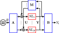
Consider SISO non-linear systems embedded in a linear feedback structure as is shown in Fig. 2. The whole system is excited by random-phase multisines with a specified PSD and PDF. Using (2), the output of the system at the bin of the DFT can be written as
| (12) |
This expression indicates that the output contains a best linear contribution to the input () and a distortion term . The goal of the DCA is to write as a sum of contributions stemming from the non-linear blocks in the circuit. has noise-like properties, as was explained in the previous section. Therefore, only the power of the output distortion, or , can be considered.
To determine the distortion contributions separately, first consider the BLAs of the different non-linear systems. All inputs and outputs of the non-linear sub-circuits are gathered frequency by frequency in column vectors and :
| (13) |
where and indicate the output and input DFT spectra of the sub-circuit respectively. The different SISO BLAs, as defined in (1), are grouped in a diagonal matrix:
| (14) |
The input-output relation of all non-linear systems can now be written simultaneously as follows:
| (15) |
Where contains the non-linear distortion introduced by the sub-systems. From here, the frequency indices and will be omitted for notational simplicity. It is shown in Appendix A that the output signal of the total system can be written as:
| (16) | ||||
Where , and are the linear blocks connected to the non-linear sub-circuits as shown in Fig. 2. is the identity matrix of size . The second part of (16) yields the expression for the output distortion as a function of the distortion in the sub-systems. Considering the power of the distortion at
| (17) |
with a row vector of length that contains the Frequency Response Function (FRF) from each distortion source to the output. The element of will be called from now on. is the covariance matrix of the distortion introduced by the non-linear sub-systems. A two-step procedure is used to obtain an estimate of , which is similar to the way we determined the BLA itself in section I [14]. First, the covariance matrix of the stacked input-output vectors is determined as in equation (10), but now and are replaced by the stacked input and output signals defined in (13). is multiplied by the number of phase realisations , as we are interested in the power of the distortion, rather than in the uncertainty on the BLA-estimate. This is now a matrix. To obtain a full-rank estimate of , the response to at least different-phase multisines must be simulated. is then calculated starting from in the following way
| (18) |
The matrix product in (17) can be re-written as:
Herein is an Hermitian matrix. The complex conjugate contributions of and will therefore combine to form a single, real-valued distortion power contribution. The expression for the distortion at the output can now be simplified as follows:
| (19) |
Equation (19) contains all the different distortion contributions: each element of the covariance matrix of the distortion sources is transferred to the output. The total distortion at the output is then the sum of all these contributions. The contributions can be sorted according to their magnitude to determine the dominant distortion contribution.
From now on, we will refer to the distortion contributions due to the diagonal elements of the distortion covariance matrix as direct distortion contributions (). The contributions due to the off-diagonal elements will be called correlation distortion contributions ().
Example 2: DCA of a non-linearity followed by its inverse
To clarify the interpretation of the different distortion contributions obtained with the BLA-based DCA, we consider the trivial example of a static non-linearity followed by its inverse. The first non-linear block is an exponential function and the second its inverse: a logarithm. The cascade of both blocks results in a perfectly linear system.
The system is excited by random-phase multisines with an which excite all frequencies up to . The rms of the multisine was set to . The steady-state spectrum for the signal , measured between the two non-linear blocks, is shown below.
![[Uncaptioned image]](/html/1610.08332/assets/x8.png)
The frequency bins excited by the multisine are shown in black, the remaining frequency lines in magenta. The measured distortion power at the internal signal is shown with the magenta line in the plot. The amount of non-linear distortion at the intermediate signal in this cascade is very high (signal to distortion ratio of ), but all the distortion is completely cancelled out by the second block, so that the input and output signals are exactly the same. We calculate the BLA of the two non-linear blocks using (9)-(11). 10000 different-phase multisines were simulated to obtain an adequately low uncertainty on the BLA-estimates in this strongly non-linear circuit.
The obtained BLAs and their uncertainty bound are shown below:
![[Uncaptioned image]](/html/1610.08332/assets/x9.png)
With these BLAs, the covariance matrix of the distortion sources can be calculated using (18). In this simple example, there are two distortion sources, one for each non-linearity. This results in a covariance matrix . The elements on the diagonal of describe the power of each of the distortion sources. The off-diagonal elements indicate the correlation between both sources. The values of the distortion covariance matrix are shown below:
![[Uncaptioned image]](/html/1610.08332/assets/x10.png)
The three distortion contributions to the output can now be calculated. The FRF from each distortion source to the output can be obtained using (16). For this example, we have:
With , and , we can calculate the distortion contributions to the output of the circuit. The direct distortion contributions due to the first stage is
The direct distortion contributions due to the second stage is
The correlation distortion contribution is given by
The obtained distortion contributions are plotted below:
![[Uncaptioned image]](/html/1610.08332/assets/x11.png)
The two direct contributions are equal in amplitude and both positive. The correlation contribution is equal to the sum of the two direct contributions, but opposite in sign. The sum of all contributions (shown in gray on the plot above) therefore lies very close to zero.
With this very simple example we have shown the effectiveness of the BLA-based DCA to predict the distortion contributions of a strongly non-linear circuit under a modulated excitation signal. Additionally, we have shown that it is important to keep the correlation distortion contributions into account to obtain a correct result.
III BLA-based DCA with S-parameters
The previous expressions can be used in a DCA on system-level simulations, where every sub-circuit is represented by a Single-Input Single-Output (SISO) system. In actual electronic circuits however, a port-based representation of the sub-blocks has to be used to represent the terminal impedances and to include the forward and reverse gain of each sub-circuit in the circuit. In the remainder of this paper, S-parameters will be used to represent the behaviour of the different circuit blocks. Similar expressions can be obtained for the Y and Z parameters, but this is considered to be outside of the scope of this paper.
The reasoning in this section is very similar to the one detailed in the previous section but, instead of working with SISO BLAs, each of the sub-circuits is described by a Multiple-Input Multiple-Output (MIMO) BLA.
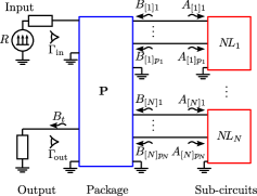
Fig. 3 shows the general circuit under test for the DCA. There are non-linear sub-circuits embedded in a package. The whole circuit is excited by different-phase multisines and the output of the circuit is terminated in a load impedance. The steady-state port voltages and currents of the sub-circuits are measured and transformed into waves using the classical expression [18]:
where is the port voltage and is the port current flowing into the sub-circuit port. is a user-chosen reference impedance. The and waves at the ports of the sub-circuit are gathered in vectors
The relation between and is given by the MIMO BLA :
is the vector of distortion sources. Determining the MIMO BLA is more complex than what has been done for the SIMO procedure described in Section I. The algorithm needed is described in the following section. For now, assume the MIMO BLA to be known. All the different BLAs are gathered in a block diagonal matrix, similarly to what was done in (15):
| (20) |
The total number of ports of all the sub-circuits is denoted by . The vector of distortion sources is again noise-like, so the covariance matrix is used to describe it. Determining is done in the same way as explained in Section II and equation (18).
The distortion at the output of the system is defined by considering the BLA from the reference multisine to the output wave :
| (21) |
The goal of the DCA is to split the power in as a sum of contributions from . Classic papers on wave-based circuit and noise analysis have dealt with this problem already ([19, 20]) and describe how to determine a row vector that is used to refer to the output wave (See appendix B).
| (22) |
This expression can be re-written in a similar way as in (19) to obtain a list of direct distortion contributions and correlation distortion contributions.
III-A Dealing with the combinatorial explosion
In circuits, each port of each sub-circuit will create several distortion contributions: a single direct contribution and some correlation contributions. The number of contributions can therefore rise quickly, especially in fully differential, complex, circuits. In a circuit with ports, there are distortion contributions to the output.
If the amount of contributions is too large to be easily tractable and interpretable, the different contributions of a single sub-circuit can be combined into a single contribution by simply summing the contributions of each of the ports of one sub-circuit. The co-variances can also be combined in the same way. Combining the contributions of each stage reduces the amount of contributions for sub-circuits to . If this amount of contributions is still too large for an easy interpretation of the results, the contributions of several sub-circuits can be combined into one contribution of a larger sub-circuit. It is a clear advantage that the BLA-based DCA can easily be applied hierarchically as this allows to zoom in selectively on the most contributing parts of the circuit, while leaving the other sub-circuits aggregated at a higher level of abstraction.
IV Estimating the MIMO BLA of sub-circuits
In the previous section, it was assumed that the Best Linear Approximation (BLA) of the sub-circuits was known. Determining the BLA is the most difficult and time-consuming step in the BLA-based DCA, as it requires averaging the large-signal steady-state response of the circuit over many different-phase multisines. For SISO sub-circuits, the estimation steps detailed in equations (9)-(11) can be used. In case of MIMO sub-circuits, extra excitation signals need to be added to the circuit to determine the BLA.
IV-A MIMO identification in feedback
The MIMO BLA of the sub-circuit with inputs and outputs, is defined as an extension of (11):
| (23) |
where is the MIMO BLA taken from the reference signals to the output waves of the sub-circuit. is the MIMO BLA from the reference signals to the input waves of the sub-circuit. Since must be invertible, at least independent reference signals have to be present in the circuit. Most circuits are only excited by one main reference signal, so the required extra reference signals have to be added artificially to the circuit to allow estimation of the MIMO BLA of the sub-circuits.
The extra multisines have to be very small in amplitude with respect to the large signal to avoid changing the BLA of the circuit, which is why they are called tickler multisines [11]. If the ticklers are placed on the same frequency grid as the main multisines, their response will be overwhelmed by the circuit response to the main multisines. To avoid this overlap, the frequency grid of the tickler is shifted by a frequency . This technique is called ’Zippering’ [21]. The zippered ticker multisines are defined by:
the phases of the tickler multisine () are drawn randomly from . These tickler multisines will create contributions on frequencies that are always away from the spectral lines of the main multisines, so the responses of the main and tickler multisines are easily separated by looking at the correct frequency bins. Because their amplitude is very small, the tickler signals can either be applied one-by-one, while the main multisine remains active, or applied all simultaneously since each of the ticklers can be given an independent .
To obtain the BLA with the zippered multisines, the SIMO BLA from each reference signal to the stacked output-input vector of the sub-circuit is determined first by simple averaging as in (9). The SIMO BLA from reference signal to the stacked output-input vector will be denoted , while its uncertainty is expressed by the covariance matrix . The are known at the frequencies of the spectral lines of multisines . All are then linearly interpolated to the spectral lines of the main multisines and gathered in a large matrix:
| (24) |
The BLA is now obtained using expression (23). To obtain the uncertainty on the BLA, the uncertainty on the -matrix is transformed by the following expression [14]:
where indicates the Kronecker product [22]. The covariance matrix contains the different covariance matrices of the SIMO BLAs on its diagonal:
Determining the MIMO BLA with the method described here can be very time-consuming because many large-signal simulations have to be run. A speed-up can be obtained using advanced non-parametric estimation techniques like the local polynomial method [23]. Alternatively, rational approximations can be estimated to reduce the noisiness of the obtained BLA estimates.
It is more easy to work with tickler current sources, as they can be added to a circuit’s netlist without introducing extra nodes. Choosing the best nodes to place the tickler multisines and determining the amplitude of the ticklers will usually require some user intervention. When the BLA from two reference signals to the the input and output waves of the circuit are too similar, the matrix will be badly conditioned and its inverse will be difficult to compute. To obtain a good conditioning of the , it is recommended to connect the tickler sources to nodes that are close to the ports of the circuit under test.
The amplitude of the tickler multisines should be small, but the circuit’s response to the tickler signal should lie above the numerical noise floor at the input and output waves. Setting the correct amplitude of the tickler signals is therefore done by increasing the amplitude of the tickler until its response is clearly visible in the steady-state spectra of all input and output signals of the sub-circuits.
In circuits with very small reverse gains, obtaining a good estimate of the reverse gain can be very difficult. For the small reverse gain, the small-signal behaviour of the sub-circuit is used if it cannot be estimated reliably [24].
Example 3: MIMO BLA of a class-C amplifier
To demonstrate how the MIMO BLA of a circuit is estimated, consider this simple class-C amplifier.
![[Uncaptioned image]](/html/1610.08332/assets/x13.png)
The class-C amplifier is excited by RPMs that excite frequencies in a band of around . Their rms value is . The transistor in the amplifier is placed in a common-source configuration, so it will be modelled by a two-port. There’s only one reference multisine in the circuit so a second multisine current source is added at the output ( shown in blue in the figure). The tickler multisines are shifted away from the frequency grid of the main multisine and are given an rms current of . The resulting wave, obtained with HB is shown below
![[Uncaptioned image]](/html/1610.08332/assets/x14.png)
The frequency bins of the main multisines are shown in black, while its distortion is shown with red. In between the frequency bins of the main multisines, the response to the tickler is visible. The frequency bins of the tickler are indicated with green, while all remaining bins are grey. The amplitude of the tickler was chosen such that the tickler response was clearly visible above the numeric noise floor.
The obtained BLAs and their uncertainty interval are shown below:
![[Uncaptioned image]](/html/1610.08332/assets/x15.png)
The dashed lines in the above plots are the small-signal S-parameters. The largest differences are observed on and , which is to be expected for a class-C biased transistor.
IV-B Weakly non-linear circuits
In weakly non-linear circuits, the BLA doesn’t deviate a lot from the small-signal frequency response of the circuits, so the small-signal behaviour can be used to replace the BLA. When the MIMO identification scheme is avoided, a significant reduction in simulation time for the DCA is obtained. The small-signal S-parameters can be obtained quickly in modern simulators combining several AC or S-parameter simulations.
Combining small-signal and large-signal results is trivial when the response of the circuit to the multisine excitations is obtained with HB. If the response is obtained with a time-domain simulation, the frequency warping should be taken into account properly:
-
-
A trapezoidal integration method should always be used to avoid artificial damping of the circuit poles [25].
-
-
A fixed time step should be used to allow calculating the spectrum easily with the DFT.
-
-
The remaining frequency warping introduced by going to the discrete time domain should be taken into account.
When the trapezoidal integration method is used, each frequency bin of the large-signal simulation is warped to a frequency according to the following relationship
| (25) |
It is as if the circuit is working on the frequency grid determined by . Hence, the small-signal behaviour should be determined on the frequency grid , or should be interpolated to the warped frequency grid to minimise errors.
When the BLA deviates too far from the small-signal S-parameters due to strongly non-linear behaviour of the circuit, one cannot replace the BLA by small-signal S-parameters without introducing errors. It is therefore important to assess the quality of the small-signal behaviour when using it to predict the distortion in the circuit. The perfect assessment could be obtained by comparing the small-signal behaviour to the estimated MIMO BLA of each sub-circuit, but calculating the MIMO BLA beats the purpose of using the small-signal behaviour in the first place. Instead, the BLA from the reference signal to the input and output waves ( as defined in (24)) can be compared to the frequency responses obtained with an AC simulation. When the difference between and the AC result lies significantly above the distortion level, the small-signal behaviour deviates too far from the correct BLA and should not be used in the DCA.
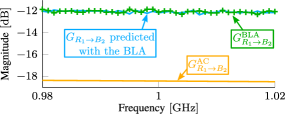
As an example, this test is applied to the class-C amplifier from before. The BLA from the main reference signal to the output wave is calculated in three different ways: First, the BLA from the reference to the output wave is calculated using the SISO techniques described in Section I. Second, the small-signal frequency response from the reference to the output wave was calculated with an AC simulation. Finally, the MIMO BLA of the transistor was used to predict the same frequency response444Appendix C explains how this is done. The three frequency responses are shown in Figure 4. The frequency response obtained with the AC simulation deviates strongly from the BLA from the reference to the output wave. When the estimated MIMO BLA is used to predict the frequency response, the correct result is obtained.
In this class-C amplifier, it is therefore not possible to use the small-signal S-parameters in the DCA, which is to be expected for such a strongly non-linear circuit. In the examples shown later, two circuits are shown where this small-signal assumption is valid.
V Examples
The BLA-based Distortion Contribution Analysis (DCA) will now be applied to several examples. First, a two-stage Miller op-amp is analysed to show the importance of the correlation between distortion sources in a real examples. With the second example, a Doherty power amplifier, the DCA is shown to work for strongly non-linear circuits as well. The weakly non-linear assumption doesn’t hold in such an amplifier, so the BLA of the sub-circuits is estimated with zippered multisines. The third and last example deals with a considerably larger circuit. The distortion contribution analysis of a a fully differential Gm-C biquad is used to illustrate how the DCA can be applied hierarchically.
V-A Miller Op-amp
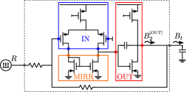
As a first example of a DCA on the circuit level, we consider a two-stage Miller-compensated op-amp designed in a commercial CMOS technology (Fig. 8). The op-amp is placed in an inverting feedback configuration with a gain of and drives a load capacitance of , resulting in a gain-bandwidth product of . The circuit is split into three sub-circuits: the input stage, which has three ports, the current mirror, and the output stage which both have two ports.
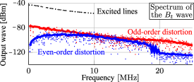
The amplifier is excited by lowpass random-odd multisines with a base frequency of and . The rms voltage of the multisines is set to . The steady-state response of the circuit to different-phase multisines is obtained by HB simulation. The obtained spectrum of the output wave is shown in Fig. 8.
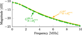
The Miller op-amp can be considered to be weakly non-linear, so the small-signal S-parameters were used to represent each sub-circuit. To test the validity of this small-signal assumption, the BLA from the reference multisine to all waves in the circuit was compared to the result obtained with an AC simulation as explained in Section (IV-B). The largest difference is observed on the frequency response from the reference to the output wave of the second stage and it is shown in Figure (8). This difference is small enough to allow using the small-signal S-parameters instead of the MIMO BLA to represent each sub-circuit.
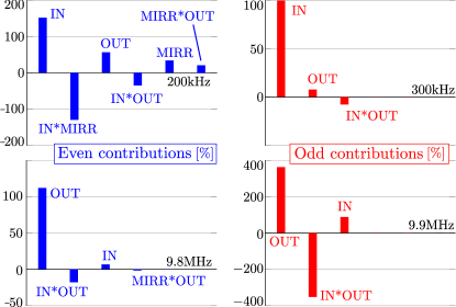
The results of the Distortion Contribution Analysis (DCA) at four different frequencies are shown in Fig. 8. The contributions are combined for each stage as was explained in Section III-A. For three sub-circuits, this results in six distortion contributions, three direct distortion contributions (one for each stage) and three correlation distortion contributions.
The even and odd distortion contributions can be split again because odd RPMs were used. At (Top left in figure 8) we obtain only even-order non-linear contributions. The input stage seems to generate the most distortion with a direct contribution which is of the total output distortion at that frequency bin, but its contribution is largely cancelled in its correlation with the current mirror, which has a contribution of of the total distortion. This leads to the output stage as the dominant source of distortion at . This shows the importance of the correlation between the distortion sources in the circuit.
In the odd-order contributions at (Top right in figure 8), the input stage is clearly the dominant generator of non-linear distortion.
The bottom series of plots in Fig. 8 shows the results at the high-frequency end of the analysed band. At , the output stage dominates the even-order contributions. At , the odd contribution of the output stage () is compensated with a co-variance with the input stage (), making the input stage the dominant source of distortion at this frequency.
With this example, we have shown that the BLA-based DCA can be used in circuit-level simulations to obtain the distortion contributions. Taking the correlation between distortion sources of different sub-circuits into account is crucial to obtain an accurate representation of the distortion in this circuit.
V-B Doherty Power Amplifier
The second example that will be considered is a Doherty power amplifier found in the example library of Keysight’s Advanced Design System (ADS). The amplifier is built with two Freescale MRF8S21100H transistors for a centre frequency of (Fig. 11). The main transistor is biased in class-AB with a quiescent current of . The auxiliary transistor is biased deep in class-C with a quiescent current of .
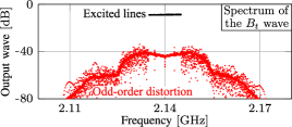
The amplifier is excited by bandpass multisines that have spectral lines in a band of around . The rms of the input multisines is . The steady-state response of the circuit to the different-phase multisine excitations is obtained by HB simulation. The output wave around the centre frequency is shown in Fig. 11.
This circuit can be considered to be strongly non-linear, especially because of the auxiliary amplifier. To obtain the BLA of the two transistors in the circuit, tickler multisines are added to the circuit at the output of the total amplifier. The added multisines are current sources which insert an rms current of on frequency bins in between the frequencies of the main multisine.
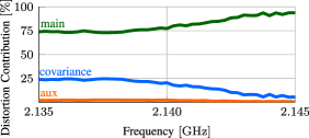
The main distortion contributor is found to be the main transistor (Fig. 11). This can be expected, as the auxiliary amplifier only kicks in for limited amounts of time in this Doherty configuration. A similar Doherty amplifier was analysed in [26] with a Volterra-based DCA under two-tone excitation555We don’t have access to the circuit simulated in [26], nor to their DCA method, so only a qualitative comparison between both methods can be obtained.. It was concluded there that the auxiliary amplifier only contributes significantly to the distortion for very high amplitudes in the two-tone. With modulated signals, like the multisines used in the BLA-based DCA, the peaks only occur from time to time, so the average contribution of the auxiliary amplifier to the total distortion is low.
The information given by the BLA-based DCA is limited for the Doherty power amplifier, because only the signals around the carrier frequency are used here. Designers are also interested in how the low-frequency signals in the bias network are up-converted in-band through the second-order non-linearities [2]. The current implementation of the DCA doesn’t split the up-converted low-frequency signals from the high-frequency odd-order non-linear distortion appearing in-band. A more advanced BLA-based DCA can be implemented using the higher-order BLAs [27]. With the higher-order BLA, one could obtain a similar result to [26], but for modulated signals, instead of two-tones.

V-C Gm-C filter
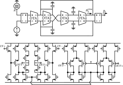
The final example is a fully differential Gm-C biquad [28] designed in the same commercial CMOS technology as the other examples (Fig. 15). Each Operational Transconductance Amplifier (OTA) in the biquad consists of an input pair and a cascode stage. The common-mode feedback in the OTA is active. The biquad is configured to create a resonant pole pair at .
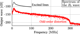
The differential mode of the biquad is excited by full lowpass RPMs (all frequency lines are excited). The multisines have and . In a resonant system like this, the frequency resolution of the multisines should be chosen to have several lines in the resonance [29]. If, for example, only a single spectral line is placed in a sharp resonance, the PDF of the internal signals will tend to that of a sine wave, instead of the wanted Gaussian PDF. The wanted noise-like properties of the internal signals in the circuit then disappear, which is unwanted if the results are to be valid for Gaussian input signals. The rms of the multisines was set to and the steady-state response of the circuit to different-phase multisines was obtained with HB. The resulting spectrum at the differential output is shown in Fig. 15. The distortion at the output lies below the signal level, so the circuit is behaving close to linear. No even-order contributions are present due to the differential nature and perfect symmetry in the simulations of the circuit. Note that the obtained odd-order distortion at the output shows a strong frequency dependence around the resonance.
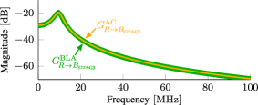
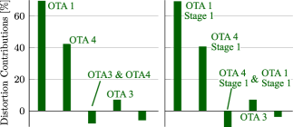
The sub-circuits in this biquad are assumed to be weakly non-linear, so the 4-port S-parameters of each OTA were used in the DCA. This small-signal assumption was verified by comparing the frequency response from the input of the total circuit to each of the waves in the circuit with the corresponding BLAs. The largest difference was observed on the frequency response from the reference to the output waves of OTA4 (shown in Figure (15)), but this difference is small enough to consider the small-signal assumption to be valid.
The first OTA is found to be the dominant source of distortion in the resonance peak of this circuit (Fig. 15, left). The fourth OTA also introduces a considerable contribution. To find out which part of the OTA is mainly responsible, the first and fourth OTA were split into two parts and the DCA was applied again. With this hierarchical application of the BLA-based DCA, it is found that the first stage of both OTAs 1 and 4 are the dominant contribution (Fig. 15 right).
With this final example, we have demonstrated how the BLA-based DCA can be used in larger circuits and how it can be used hierarchically to zoom in on certain sub-circuits to determine the actual source of non-linear distortion.
VI Conclusions
Combining the Best Linear Approximation (BLA) with a noise analysis creates a Distortion Contribution Analysis (DCA) that pin-points the sources of non-linear distortion in a circuit under excitation of complex, modulated signals. The method doesn’t require special models and can be implemented easily with the help of a few post-processing steps on top of a commercial simulator.
The BLA-based DCA works for both weakly and strongly non-linear circuits, returns a single distortion contribution for each sub-circuit and takes the correlation between the distortion introduced by the sub-circuits into account. The method can be applied hierarchically and therefore suitable to be applied to large circuits without introducing hundreds of contributions.
The method has been demonstrated on several examples and is shown to be able to provide information about the source of non-linear distortion in a two-stage op-amp, a Doherty power amplifier and a fully differential gm-C filter.
Acknowlegment
This work is sponsored by the Vrije Universiteit Brussel, dept. ELEC, Pleinlaan 2, 1050 Brussels, Belgium, Fund for Scientific Research (FWO-Vlaanderen), Institute for the Promotion of Innovation through Science and Technology in Flanders (IWT-Vlaanderen), the Flemish Government (Methusalem), the Belgian Federal Government (IUAP VII) and the Strategic Research Program of the VUB (SRP-19)
Appendix A Obtaining expression (16)
In the circuit shown in Figure 2, the following equations describe the behaviour of the input, output and feedback dynamics:
| (26) | ||||
| (27) |
The relation between and is given by the BLA
| (28) |
Plugging equation (26) into (28) and solving for , we obtain
Using this expression in (27) and grouping the terms in and yields equation (16).
Appendix B DCA with S-parameters
To calculate the contributions of the distortion sources to the output of the circuit, an algorithm similar to the one described in [20] is used. The different S-matrices of the components in the circuit shown in Fig. 3 are gathered in a matrix , while the distortion sources are gathered in a vector :
where and are the reflection factors presented to the circuit by the reference source and load respectively. is the block diagonal matrix of size which contains the BLAs of the circuits as defined in equation (20). is the vector of distortion sources of length defined in the same expression. is the S-matrix of the package defined in Figure 3 of size for a circuit with external ports.
The interconnection between the different parts of the circuit is represented by the following matrix:
The incident-waves at all ports generated by the sources in is given by the following expression
| (29) |
Since we are only interested in the wave incident to the load, just the second row of is used. Also, the first elements of can be ignored, because the first elements of are zero. This finally leads to the expression for used in equation (22)
| (30) |
Appendix C Predicting the BLA from reference to the waves in the circuit
Predicting the frequency response from the main reference signal to the input and output waves at the ports of the sub-circuits is done using the same matrix as was used in Appendix B. but now, the -vector is set to the following:
where is the chosen reference impedance and is the reflection factor presented by the reference source. All A-waves in the circuit are now predicted by (29). The frequency response from the reference voltage source to the A-waves radiating into the sub-circuits are found at . The frequency response from the reference voltage source to the B-waves at the ports of the sub-circuits are found at .
References
- [1] P. Wambacq and W. Sansen, Distortion Analysis of Analog Integrated Circuits. Kluwer, 1998.
- [2] J. P. Aikio and T. Rahkonen, “Utilization of distortion contribution analysis,” in Circuit Theory and Design (ECCTD), 2011 20th European Conference on, Aug 2011, pp. 701–704.
- [3] S. Narayanan, “Transistor distortion analysis using volterra series representation,” The Bell System Technical Journal, vol. 46, no. 5, pp. 991–1024, May 1967.
- [4] J. Aikio and T. Rahkonen, “Detailed distortion analysis technique based on simulated large-signal voltage and current spectra,” IEEE Transactions on Microwave Theory and Techniques, vol. 53, no. 10, pp. 3057–3066, Oct 2005.
- [5] L. De Locht, Y. Rolain, and G. Vandersteen, “Designing power amplifiers? use good excitation signals,” in Proceedings of the 67th ARFTG Conference, June 2006, pp. 211–213.
- [6] L. De Locht, G. Vandersteen, P. Wambacq, Y. Rolain, R. Pintelon, J. Schoukens, and S. Donnay, “Identifying the main nonlinear contributions: use of multisine excitations during circuit design,” in Proceedings of the 64th ARFTG Conference, Dec 2004, pp. 75–84.
- [7] L. Bos, G. Vandersteen, Y. Rolain, and R. Pintelon, “Analysis and modelling of mixed-data systems with frequency translation using multisine excitations,” in Proceedings of the 2008 Instrumentation and Measurement Technology Conference (IMTC 2008), may 2008, pp. 542 –546.
- [8] S. Bronckers, G. Vandersteen, J. Borremans, K. Vandermot, G. Van der Plas, and Y. Rolain, “Advanced nonlinearity analysis of a 6 GHz wideband receiver,” in Proceedings of the 2008 Instrumentation and Measurement Technology Conference (IMTC 2008), may 2008, pp. 1340 –1343.
- [9] G. Vandersteen and L. De Locht, “Qualification and quantification of the nonlinear distortions in discrete-time sigma-delta adcs,” in Proceedings of the European Conference on Circuit Theory and Design (ECCTD), Aug 2009, pp. 759–762.
- [10] A. Cooman, E. Geerardyn, G. Vandersteen, and Y. Rolain, “Determining the dominant nonlinear contributions in a multistage op-amp in a feedback configuration,” in Proceedings of the 2012 International Conference on Synthesis, Modeling, Analysis and Simulation Methods and Applications to Circuit Design (SMACD), september 2012.
- [11] L. De Locht, “Measuring, modeling and realization of high-frequency amplifiers,” Ph.D. dissertation, Vrije Universiteit Brussel (VUB), 2007.
- [12] R. Pintelon and J. Schoukens, System Identification a frequency domain approach, 2nd ed. John Wiley & Sons, Inc., 2012.
- [13] ——, “FRF measurement of nonlinear systems operating in closed loop,” IEEE Transactions on Instrumentation and Measurement, vol. 62, no. 5, pp. 1334–1345, May 2013.
- [14] R. Pintelon, G. Vandersteen, J. Schoukens, and Y. Rolain, “Improved (non-)parametric identification of dynamic systems excited by periodic signals the multivariate case,” Mechanical Systems and Signal Processing, vol. 25, pp. 2892 – 2922, 2011.
- [15] N. B. Carvalho, K. A. Remley, D. Schreurs, and K. G. Card, “Multisine signals for wireless system test and design [application notes],” IEEE Microwave Magazine, vol. 9, no. 3, pp. 122–138, June 2008.
- [16] R. Pintelon, G. Vandersteen, L. D. Locht, Y. Rolain, and J. Schoukens, “Experimental characterization of operational amplifiers: A system identification approach. part I: Theory and simulations,” IEEE Transactions on Instrumentation and Measurement, vol. 53, no. 3, pp. 854–862, June 2004.
- [17] A. Cooman, G. Vandersteen, and Y. Rolain, “Finding the dominant source of distortion in two-stage op-amps,” Analog Integrated Circuits and Signal Processing, vol. 78, no. 1, pp. 153–163, Januari 2013.
- [18] K. Kurokawa, “Power waves and the scattering matrix,” IEEE Transactions on Microwave Theory and Techniques, vol. 13, no. 2, pp. 194–202, Mar 1965.
- [19] V. Monaco and P. Tiberio, “Computer-aided analysis of microwave circuits,” Microwave Theory and Techniques, IEEE Transactions on, vol. 22, no. 3, pp. 249–263, Mar 1974.
- [20] J. A. Dobrowolski, “A cad-oriented method for noise figure computation of two-ports with any internal topology,” Microwave Theory and Techniques, IEEE Transactions on, vol. 37, no. 1, pp. 15–20, Jan 1989.
- [21] K. Vanhoenacker, T. Dobrowiecki, and J. Schoukens, “Design of multisine excitations to characterize the nonlinear distortions during frf-measurements,” in Proceedings of the 17th IEEE Instrumentation and Measurement Technology Conference (IMTC), vol. 3, 2000, pp. 1254–1259 vol.3.
- [22] J. Brewer, “Kronecker products and matrix calculus in system theory,” IEEE Transactions on Circuits and Systems, vol. 25, no. 9, pp. 772–781, Sep 1978.
- [23] R. Pintelon, J. Schoukens, G. Vandersteen, and K. Barbé, “Estimation of nonparametric noise and FRF models for multivariable systems part I: Theory,” Mechanical Systems and Signal Processing, vol. 24, no. 3, pp. 573 – 595, 2010.
- [24] A. Cooman, P. Bronders, and G. Vandersteen, “Distortion contribution analysis of strongly non-linear analog circuits,” in Proceedings of the 2016 International Conference on Synthesis, Modeling, Analysis and Simulation Methods and Applications to Circuit Design (SMACD), 2016.
- [25] K. S. Kundert, The Designer’s Guide to Spice and Spectre. Kluwer Academic Publishers, 1995.
- [26] J. P. Aikio, “Distortion contribution analysis of an LDMOS doherty power amplifier,” in Proceeding of the Workshop on Integrated Nonlinear Microwave and Millimetre-Wave Circuits (INMMIC), Sept 2012, pp. 1–3.
- [27] M. Thorsell, K. Andersson, G. Pailloncy, and Y. Rolain, “Extending the best linear approximation to characterize the nonlinear distortion in GaN HEMTs,” IEEE Transactions on Microwave Theory and Techniques, vol. 59, no. 12, pp. 3087–3094, Dec 2011.
- [28] J. E. Kardontchik, Introduction to the design of transconductor-capacitor filters. Kluwer Academic Publishers Group, 1992.
- [29] E. Geerardyn, Y. Rolain, and J. Schoukens, “Design of quasi-logarithmic multisine excitations for robust broad frequency band measurements,” IEEE Transactions on Instrumentation and Measurement, vol. 62, no. 5, pp. 1364–1372, May 2013.
![[Uncaptioned image]](/html/1610.08332/assets/28C__Users_Adam_Google_Drive_Contributies_CAS_paper_pics_biopicAdam.jpg) |
Adam Cooman (1989, Belgium) graduated as an Electrical Engineer in Electronics and Information Technology in July 2012 at Vrije Universiteit Brussel (VUB). In August 2012 he joined the department ELEC as a PhD student. His main interests are the design of analog/RF circuits and non-linear modelling. |
![[Uncaptioned image]](/html/1610.08332/assets/29C__Users_Adam_Google_Drive_Contributies_CAS_paper_pics_biopicPiet.jpg) |
Piet Bronders (1991, Fiji) graduated as an Electrical Engineer in Electronics and Information Technology in 2014 at the VUB. In October 2014 he joined the department ELEC as a PhD student. His main interest is NL RF circuit design and measurement. His current research topic is the design and modelling of RF power amplifiers. |
![[Uncaptioned image]](/html/1610.08332/assets/30C__Users_Adam_Google_Drive_Contributies_CAS_paper_pics_biopicDries.png) |
Dries Peumans (1992, Belgium) graduated as an Engineer in Electronics and Information Technology in 2015 at the VUB. Afterwards he joined the department ELEC as a PhD researcher. His research focuses on non-linear modelling and the design of analog circuits. |
![[Uncaptioned image]](/html/1610.08332/assets/31C__Users_Adam_Google_Drive_Contributies_CAS_paper_pics_biopicGerd.jpg) |
Gerd Vandersteen (1968, Belgium) received the degree in electrical engineering in 1991 and his PhD in electrical engineering in 1997, both from the VUB, Brussels, Belgium. During his postdoc, he worked at the micro-electronics research centre IMEC as Principal Scientist in the Wireless Group with the focus on modelling, measurement and simulation of electronic circuits in state-of-the-art silicon technologies. This research was in the context of a collaboration with the VUB. From 2008 on, he is working as Prof. at the VUB in the department ELEC within the context of measuring, modelling and analysis of complex linear and non-linear system. Within this context, the set of systems under consideration is extended from micro-electronic circuits towards to all kinds of electro-mechanical systems. From 2011 on, he is director of the Doctoral School of Natural Sciences and (Bioscience) Engineering (NSE) at the VUB |
![[Uncaptioned image]](/html/1610.08332/assets/32C__Users_Adam_Google_Drive_Contributies_CAS_paper_pics_biopicYves.jpg) |
Yves Rolain (1961, Belgium) received the Electrical Engineering (Burgerlijk Ingenieur) degree in July 1984, the degree of computer sciences in 1986, and the PhD degree in applied sciences in 1993, all from the VUB, Brussels, Belgium. He is currently a research professor at the VUB in the department ELEC. He became a fellow of the IEEE in 2006 and received the IEEE I&M Society award in 2005. His main interests are microwave measurements and modelling, applied digital signal processing and system identification. |