Generation of Schrödinger’s cat states in a planar semiconductor heterostructure
Abstract
We propose a nanodevice based on a typical planar semiconductor heterostructure with lateral confinement potential created by voltages applied to local gates. We show how to obtain near parabolical confinement along the nanodevice, and how to use coherent states of the harmonic oscillator for spatial separation of electron densities corresponding to opposite spin directions. In such a way, an entangled state of Schrödinger’s cat type is created. We have performed simulations of a realistic nanodevice model by numerical solving the time-dependent Schrödinger’s equation together with simultaneous tracking of the controllable confinement potential via solution of the Poisson’s equation at every time step.
pacs:
I Introduction
Control and manipulation of single electrons trapped in semiconductor nanostructures attract much attention due to potential applications in spintronics Hanson et al. (2007); Žutić et al. (2004) or quantum computing Ladd et al. (2010). This also enables us to examine numerous fundamental physical phenomena and discover a new physics, e.g. topological effects Hasan and Kane (2010); Zhang and Nori (2015) or exotic quasi-particles Fu and Kane (2008); Lutchyn et al. (2010); Klinovaja et al. (2012); Oreg et al. (2010).
An electron qubit can be represented in many different ways Owen et al. (2014). In the case of a charge qubit Bertoni et al. (2000); Hayashi et al. (2003); Petersson et al. (2010), two basis states are defined as the presence of an electron on one of two sides of a double quantum dot or wire structure. However, it is more likely that the spin degree of freedom will be used as a bit carrier in the quantum computer, i.e. spin qubitLoss and DiVincenzo (1998); Kloeffel and Loss (2013). This explains the necessity for precise electron control to perform operations on such qubits, or to couple them into registers Shulman et al. (2012); Trifunovic et al. (2012, 2013); Pal et al. (2015); Mehl and DiVincenzo (2015); Hassler et al. (2015); Szumniak et al. (2015), and transmit information between individual registers of the quantum computer Bednarek et al. (2008a); Bednarek and Szafran (2009); Bednarek et al. (2010); Bednarek and Szafran (2008). Spin-orbit interaction (SOI) of Rashba type (RSOI) Rashba (1960); Bychkov and Rashba (1984a, b); Winkler (2003), which couples the orbital and spin degrees of freedom of an electron, allows for effective manipulation of a spin qubit Nowack et al. (2007); Nadj-Perge et al. (2010, 2012); Malard et al. (2011); López et al. (2012); Ban et al. (2012); Čadež et al. (2014); Szaszkó-Bogár et al. (2015); Pawłowski et al. (2016a, 2014).
An important issue in quantum computing is the generation of entangled states. The Schrödinger’s cat state is a notable example Wineland (2013); Lau et al. (2014); Ralph et al. (2003); Liao et al. (2016). This has been successfully generated in quantum optics using coherent states Monroe et al. (1996); Leibfried et al. (2003); Myatt et al. (2000); Sackett et al. (2000); Jeong and Kim (2002). The possibility to create coherent states has also been examined in solid-state systems Owen et al. (2012, 2014); Pyshkin et al. (2016); Liao et al. (2016); Kataoka et al. (2009); Pawłowski et al. (2016b). However, creation of their combination with opposite spin, namely the Schrödinger’s cat state, poses a great challenge due to its high instability Wineland (2013); Blatt and Wineland (2008); Myatt et al. (2000); McDonnell et al. (2007).
In this paper, we propose to repeat these quantum optics experiments in a solid state system. We show the possibility for the creation of a Schrödinger’s cat state in a typical and easily obtainable semiconductor heterostructure. This is an extension to the method introduced in [Pawłowski et al., 2016b], here developed on heterostructures, which are much more easily scalable. Control over an electron is achieved all electrically by applying voltages to local gates. The spin separation of coherent states, forming in superposition the Schrödinger’s cat state, is achieved in the nanostructure with an electrically controlled Rashba spin-orbit coupling.
The paper is organized as follows. In the first part (Sec. II) of the article we employ a one-dimensional (1D) approximation with modeled potentials and the method for the generation of the Schrödinger’s cat state is discussed only qualitatively. In the latter part (Sec. III) we propose a nanodevice based on a planar semiconductor heterostructure. The design includes geometrical details and the realistic values for parameters of the materials used. Potentials are calculated using the Poisson’s equation with all important effects included. The results from this part are quantitative in nature.
II Explaining the effect with a simplified model
II.1 Simplified one-dimensional model
The Hamiltonian of a single electron trapped in a quantum wire—a 1D structure—oriented along the -axis has the following form:
| (1) |
where constitutes the potential energy of an additional confinement along the wire and describes the spin-orbit interaction. If the quantum wire axis is oriented in the crystallographic direction, the Dresselhaus interaction becomes negligible Nadj-Perge et al. (2012); Winkler (2003). Now if we apply an electric field along the -axis, an RSOI is introduced. It can be described by the following Hamiltonian:
| (2) |
with the RSOI material coefficient , the electric field perpendicular to the wire direction, and the electron momentum operator together with the the Pauli -matrix .
If the confinement potential along the wire has a parabolic shape , we can solve the eigenequation of the Hamiltonian (1) analytically in the momentum representation and then return to the position representationPawłowski et al. (2016b). The energy of the ground state is doubly degenerated with respect to spin values. The ground state wavefunction in the position representation takes the form of a Gaussian multiplied by a plane wave. Depending on the spin -projection its wavenumber is either positive or negative. The two basis functions corresponding to the ground state have the two-row spinor form
| (3) | ||||
| (4) |
with and the wavenumber .
We should note that the wavenumber does not depend on the harmonic potential curvature (frequency ). Indeed, for any confinement potential the eigenstate of (1) has the general form , where is an eigenfunction calculated without the spin-orbit interaction. SOI introduces a spin-dependent displacement in the momentum (space). Due to the degeneration, any linear combination of both basis states corresponds to the same energy. The SOI merely introduces an energy correction .
II.2 Semiconductor electron soliton – an inducton
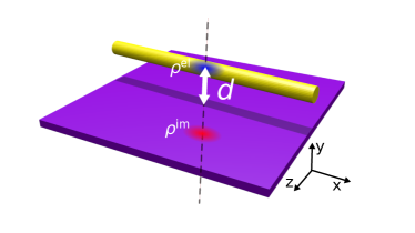
We assume that the quantum wire is aligned in parallel to a metallic gate, as shown in Fig. 1. If we trap an electron inside the wire, an opposite charge will be induced on the surface of the conductor. This effect can be described within the mean field self-consistent approximationBednarek et al. (2005). The induced charge attracts the electron and causes the mean electric field to have a component directed toward the center of the electron density, resulting in a self-focusing of the electron wavefunction. Thus, an electron soliton called an inductonBednarek et al. (2005); Bednarek and Szafran (2006) is formed. The electron becomes trapped under the gate, creating a stable Gaussian-like wavepacket of finite size, capable of moving without changing its shape. Because of such localization we can relocate the electron within the wire in a controllable manner Bednarek et al. (2008a); Bednarek and Szafran (2009); Szumniak et al. (2012). Moreover, inductons and their spins can be used as quantum bit carriers in the quantum computer Bednarek and Szafran (2006); Szumniak et al. (2015); Bednarek and Szafran (2009); Szumniak et al. (2012).
This mean field, in which the electron is located, is generated by the electron (charge) itself. Thus, the field is calculated in a self-consistent way. If the gate is an infinite conducting plate, the potential created by the induced charge can be described using the image charge method. The induced charge is replaced by an image charge which is a reflection (against the surface of the conductor) of the primary charge density from the quantum wire Bednarek et al. (2005). For a quantum wire placed at distance from the conducting plate, the potential energy created by interaction with the image charge can be expressed in the following way:
| (5) |
with the image charge density being a mirrored version of the electron charge from the quantum wire —see Fig. 1, and calculated as
| (6) |
If there is no additional external potential in (Eq. 1), only the interaction energy with the image charge is present: . Since the image charge method is applicable only for cases of an infinite interface between a dielectric medium and a metallic plate, this approach is used only for model potentials in the first part of this article (Sec. II). For actual realizations of the nanodevice (Sec. III), the potential inside the quantum wire is exactly calculated using the Poisson’s equation. This method is slightly more complex; however, it guarantees correct inclusion of the induced charge on gates of any shape or dimension Bednarek et al. (2008b).
The potential energy for the electron ground state, originating from the induced charge present on the gate parallel to the quantum wire, takes an approximately parabolic shape Bednarek et al. (2005). Therefore, if this potential energy, and the SOI generated by the electric field are taken into account, the wavefunction of the electron ground state in the wire is a Gaussian multiplied by a plane wave as in (Eqs. 3 or 4). As noted, we get such multiplied eigenfunctions for any form of the confining potential, also for the induced one .
II.3 Control of the electron motion
Let us assume that the electron spin is directed along the -axis (spin -projection ) with a nonzero electric field . In such a case the ground state wavefunction assumes the form of (Eq. 3). This is a stationary state and the wavepacket remains fixed even though the wavefunction is a Gaussian multiplied by a plane wave. This happens because motion is blocked by the SOI included in the Hamiltonian. However, if we disable the electric field abruptly (in a non-adiabatic manner), inserting , the SOI disappears and the electron starts moving in the -direction. Now the wavefunction is a gaussian multiplied by a plane wave. Such a wave packet travels at a constant speed :
| (7) |
with . Let us note that after inserting this time-dependent wavefunction (7) into the expression (6), the image charge density moves at the same speed . Inserting this into (Eq. 5) gives a time-dependent potential obeying a similar relation
Thus the induced potential follows the wave packet at the same speed. This allows both the wave packet and the potential for moving in space without changing shape. In other words, the nonlinear Schrödinger equation with the potential is Galilean invariant in sense, that if is a stationary solution, the time-dependent is also its solution.
Setting back to the previous value stops the electron again, while using a greater value for forces movement in the opposite direction. Thus, we gain a method to control the electron motion using an electric field perpendicular to the direction of motion. The time evolution of the electron packet is obtained by numerically solving the time-dependent Schrödinger equation , for the Hamiltonian (1) with variable spin-orbit part . The Schrödinger equation is solved self consistently with the induced potential, which in turn depends on the electron density . In the latter part (Sec. III) this will be replaced by self consistency with the Poisson equation.
Now we assume that the ground state is generated with . This time the wavefunction is again a Gaussian but no longer multiplied by a plane wave (). We propel the electron by setting non-zero . Fig. 2 shows an electron motion induced by changes of the electric field. The black curve denotes the value of , the blue curve denotes the expectation value of position , the solid red one denotes the expectation value of momentum and the dashed red one denotes the classical momentum calculated as a time derivative of the position multiplied by the electron mass .
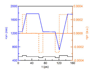
Initially, we apply no electric field () and the electron remains stable. At ps we set a positive value for , which sets the electron in motion in the direction of positive values of . At ps, we set the electric field back to zero and the electron halts. Finally at ps, the electric field is set to , which induces movement toward negative values of . Further manipulation of the electric field alters the velocity and the direction of the electron motion. We should notice that, despite the movement occurring at various velocities (corresponding to different values of the classical momentum ), the expectation value of momentum operator remains zero, which means that the wavefunction is only a Gaussian, yet not multiplied by a plane wave (). However, if the electric field is non-zero (SOI present), this state is no longer stationary. Therefore, the electron motion is initiated as a result of the change of the Hamiltonian, and not the wavefunction.
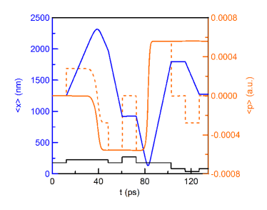
The situation changes significantly if we allow the electron to reflect off the wall of the potential formed at the wire ends. In the Fig. 3, we can track the motion of the electron in such a case with reflections occurring at ps and ps. After reflection, the electron moves with the same speed but in the opposite direction to the initial one. This indicates that the wavefunction has been effectively multiplied by a plane wave with a doubled wavenumber . The expectation value of the momentum operator is no longer zero, but still inconsistent with the classical momentum . At the moment ps, the directions of both these quantities are actually opposite to each other.
II.4 Accelerating the electron – a synchrotron
The change of the wavefunction due to reflection can be exploited for wavepacket acceleration. In Fig. 4 we see a simulation of the electron motion induced in a rectangular potential well by square pulses of the electric field. The pulses have constant amplitude and duration carefully tuned to the moment of transition of the wavepacket through the central point of the wire. With every change of direction of the electric field, the electron is being accelerated.
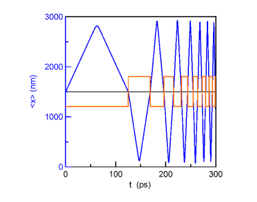
With increasing speed of the electron, the time between reflections decreases; hence, the changes of the electric field must be performed at decreasing periods of time.
This inconvenience can be mitigated by putting the electron in an external parabolic confinement potential , making . In this case, with no SOI, the ground state wavefunction of the electron assumes a Gaussian form:
| (8) |
Note that parameter is renormalized by self-interaction, while eigenfrequency remains . Multiplication of this Gaussian by a plane wave sets the electron in an oscillatory motion with an amplitude dependent on , yielding
| (9) |
Fig. 5 shows the motion of the electron initially set as the ground state of the harmonic oscillator, without SOI but multiplied by a plane wave with three different values for .
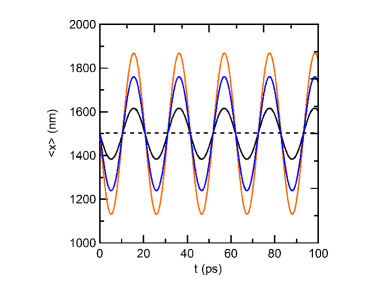
Regardless of the actual value of the wavenumber (and energy) the periods of oscillations remain the same, as for a classical particle. This effect can be used for motion synchronization.
If the electron is confined in a harmonic potential with additional spin-orbit coupling, varying sinusoidally with frequency consistent with the frequency of the harmonic potential, we can accelerate the electron to high velocities using only low gate voltages (and thus we obtain a synchrotron-like device). This can be achieved using a sinusoidally oscillating electric field applied in the area occupied by the electron. The Fig. 6 shows the motion of the wavepacket subjected to such a field. In the time interval between ps and ps the expectation value of the position (blue curve) oscillates with a linearly increasing amplitude. The energy (red curve) rises quadratically in a step-wise manner, because the wavenumber rises by the same value with each oscillation of position. These results are in analogous to the classical harmonic oscillator with resonant driving where amplitude linearly increases over time.
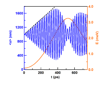
An increase in the position oscillations amplitude, and hence also in energy, requires an exactly parabolical confinement potential. Non-parabolicity constitutes a natural limit to energy growth. In the simulation shown in Fig. 6, the wavepacket is confined in a parabolic potential but the calculations are performed on a finite fragment of the quantum wire which effectively imposes infinite potential walls at both ends of the wire. As the electron approaches the wire borders, the frequency of its oscillations is no longer consistent with the frequency of the time-varying electric field inducing its movement. The amplitude of spatial oscillations of the wavepacket ceases to grow. The influence of nonparabolicity is easily visible in Fig. 6 for ps.
In all the presented simulations we assumed that initially the electron spin is parallel to the -axis. Despite the electron movement, the spin did not change, since according to the Hamiltonian (Eq. 2), movement along the -axis implies rotation of spin around the -axis. The situation would be similar if the initial spin was antiparallel to the -axis. It would only result in an opposite direction for the electron movement.
II.5 Spin density separation
Now let us assume that the spin of the electron is neither parallel nor antiparallel to the -axis, but is a linear combination of both basis vectors (Eqs. 3, 4), forming the two-row spinor:
| (10) |
As mentioned before, after the SOI is turned on, the upper and lower parts of the spinor gain opposite momenta; hence, this effect can be used for spatial spin separation.
This time, we initially set up the electron spin as an equally weighted linear combination of spins up and down. Moreover, the electron is trapped in a parabolic potential and we initialize it as the ground state of the harmonic oscillator with an assumption of no SOI (); thus, the wavefunction is of the form:
| (11) |
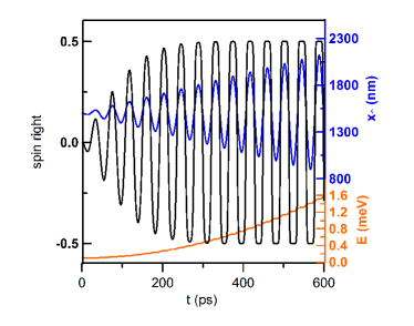
Next, we apply an electric field varying sinusoidally with the frequency tuned to the eigenfrequency of the chosen harmonic potential. Both parts of the spinor behave in different ways, such as wavefunctions of the electron with spin up and down (Eq. 3, 4). The center of mass of the entire electron does not move; however, if calculated for each spinor component respectively, they move away in an oscillatory fashion with opposite phases and growing amplitude. In Fig. 7, we see the time evolution of such a system. The expectation value of position for the spin up (blue curve) is calculated using the upper component of the spinor (Eq. 10) as
| (12) |
with being the length of the quantum wire. The oscillations of the center of mass of the electron density with spin down (not presented) are similar, but with a phase shifted by . The expectation value of the Pauli- matrix (black curve), calculated in the right half of the quantum wire, is
| (13) |
and denoted by spin right in the figures.
The expectation position of the upward spin density oscillates similar to the expectation value of position of the electron from Fig. 6. In the parabolic region of the potential, the amplitude of oscillations grows linearly with time. As the oscillations of spin up and down wavefunctions are phase-shifted by exactly , these components separate. Now let us look at the orientation of spin in the right half of the quantum wire (black curve). The amplitude stops growing as it reaches the value (or ), meaning that the entire spin in the right half is oriented upwards (downwards). For better visualization we can define the spatial -spin component density as
| (14) |
and compare it with the total electron density defined as
| (15) |
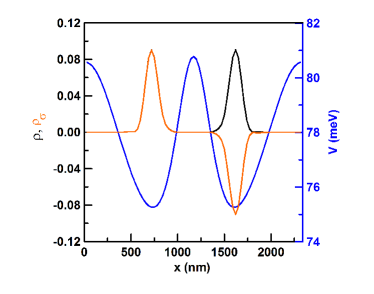
Fig. 8 shows a comparison of the spin density (red curve) and the total density (black curve) at the moment of maximal spin separation (spin in the right half reaching ).
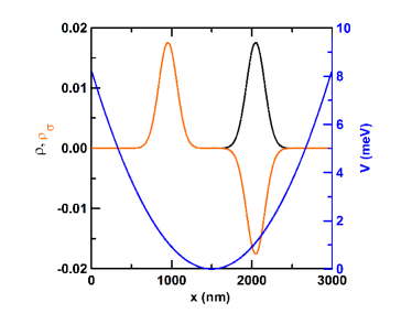
In the left part of the wire the spin density completely covers the total density, meaning that in this region the spin is oriented upwards. Consequently, the right half contains the spin oriented downwards. Now, if we put a potential barrier in the center of the quantum wire, the spin density divides into two spatially separated parts with opposite spins.
We should also notice that, as the amplitude of oscillation of the spin up position increases, the course of the spin in right half of the wire (black curve in the Fig. 7) starts to form plateaus and resemble a square wave. Therefore, time intervals with separated spins (plateaus) become longer compared to the intervals of spin changes. This increases the tolerance for the moment of the potential barrier creation. Fig. 9 shows the results of a simulation, in which a potential barrier was created in the center of the potential well at about ps.
The wavefunction of the electron state shown in Fig. 8 is of Schrödinger’s cat type Monroe et al. (1996); Wineland (2013) and it can be written as with states and denoting spin orientations, and states and denoting localization of the electron, respectively, in the left and right half of the quantum wire. After separation of both parts of the spin density with a potential barrier, the parts can be relocated to arbitrary positions and the wavefunction still describes the Schrödinger’s cat state. Such a wavefunction also has another important feature, that is, it constitutes an entangled state of spin state and state localized in two different spatial regions Wineland (2013). This state has been observed experimentally in ion traps Monroe et al. (1996); Myatt et al. (2000); Turchette et al. (2000); McDonnell et al. (2007). The purpose of our study is to design a nanodevice based on a planar semiconductor heterostructure in which this effect could be observed.
In simulations presented in Figs. 2-6, we have shown movement of the electron as a whole. In this case, self-focusing was beneficial, since it stabilizes the shape of the wavepacket. Its influence was calculated with the image charge method under the assumption that distance between the quantum wire and the metallic gate was equal to nm. In the subsequent simulations (Figs. 7-9) the self-focusing effect disturbs the spin separation process and had to be eliminated. During separation both parts of opposite spins interact with each other through the induced charge. The interaction potential is nonparabolic and destroys the parabolicity of the total confinement potential effectively changing the frequency of oscillations. The self-focusing was mitigated by placing the quantum wire at a greater distance from the gate (we assumed nm). During the design stage of a real nanodevice we cannot proceed this way and self-focusing has to be compensated in a different manner.
III Nanodevice generating Schrödinger’s cat states
III.1 Nanodevice design and principles of simulation
For practical realization of the nanodevice we propose a typical gated planar semiconductor heterostructure grown in the direction, with a quantum well (QW) parallel to its surface (, plane). The Fig. 10 shows a schematic view of the proposed nanodevice.
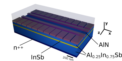
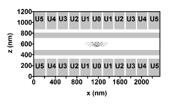
The QW is made of which has a relatively high Rashba coupling. Two blocking layers, below and above the QW, are made of ternary with , for which the bottom of the conduction band is shifted up by meV, creating potential barriers Dai et al. (2000, 1998); Gouider et al. (2010). The substrate may consist of highly doped with donors (n++). The lower blocking layer is nm thick, while the upper one is of a thickness of nm. The InSb QW inbetween is nm thick. An array of gates, as depicted in Fig. 11 ( denotes the -position of the QW), is deposited on the heterostructure. Similar, somewhat complex, gate layouts can be found in various experimental worksZajac et al. (2016); Shulman et al. (2012); Granger et al. (2015); Ward et al. (2016), being successfully deposited on a surface of a heterostructure. Moreover, the top of the structure is covered with a layer of dielectric material (AlN) of thickness nm. Finally, we put an additional layer of metal on the dielectric (not shown in the picture).
We choose InSb for the quantum well material, as it is characterized by a large value of spin-orbit coupling , which allows for effective generation of cat states in times much shorter than the coherence time of the spin-qubit. The choice of InAs with a several times smaller value of would increase several times the time of operation of the device.
If there is no electric field, the electrons fill the QW up to the Fermi level, creating a two dimensional electron gas (2DEG). Electrons trapped in the QW have two degrees of freedom in lateral directions ( and ). By applying negative voltages to gates (in relation to the substrate) we can remove the 2DEG from the quantum well leaving only one electron trapped between two long central gates (rails). The voltages applied to the rails block electron movement along the -axis. To the remaining gates, we apply voltages creating a parabolic confinement potential along the -axis.
The potential distribution in the nanodevice is calculated by solving the Poisson’s equation in a computational box surrounding the entire device. To simplify the boundary conditions setup, we covered the entire structure with a layer of metal, although it does not have any considerable impact on the operation of the nanodevice. We have chosen a computational box with dimensions nm, nm, nm as optimal. In the simulations we consider all the complexity of the structure by including the geometry details, voltages applied to the substrate and gates, the time-dependent distribution of the electron in the QW, and also the charge induced on the gates or the (conducting) substrate.
The confined electron is treated as a particle in a 2D QW with a motion frozen in the direction; hence, we assume a time-dependent Hamiltonian of the form:
| (16) |
Here denotes the effective band mass of an electron in material, and constitutes the potential felt by the electron calculated as
| (17) |
with being the total potential inside the nanodevice calculated at each time step using the generalized Poisson’s equation
| (18) |
This is solved with boundary conditions created by voltages applied to the gates. The charge distribution is calculated as in (Eq. 15), but here in three dimensions. We also need to subtract the Coulomb potential, originating directly from the electron distribution, from the total potential to avoid electron self-interaction. This is calculated as
| (19) |
Details of this method can be found in [Bednarek et al., 2008a]. The last term of (Eq. 16) constitutes the RSOI given by the following HamiltonianBychkov and Rashba (1984a, b); Winkler (2003):
| (20) |
with two-dimensional electron momentum and the Rashba coupling for materialWinkler (2003). The Pauli vector .
The value of the Rashba coupling strictly depends on quantum well material (InSb) parameters. It may also depend on the barrier material and details of the electron confinement within the heterostructure in direction. The exact coupling calculations and the validity of the used Rashba model have been included in the appendix. If the InSb layer is grown in the [111] crystallographic direction, the Dresselhaus spin-orbit interaction HamiltonianDresselhaus (1955); Hanson et al. (2007); Studer et al. (2010) can be reduced to a pure Rashba-like term: .Ye et al. (2012) Such a term adds a constant offset to the Rashba coupling and does not affect the presented spin density separation process.
We apply voltages to the gate array depicted in the Fig. 11. Initially the rails and the top gate (not visible) are set to mV. To the side gates located in the center of the structure (gates ) we apply voltages mV lower ( mV). Voltages for the remaining side gates are calculated as with mV. The zero reference voltage is applied to the doped substrate.
Now, we generate the ground state of an electron using the imaginary time evolution method Davies et al. (1980). Then, during the real time evolution of the system we change sinusoidally the voltages applied to all the gates, according to the formula
| (21) |
with mV, mV and tuned to the characteristic frequency of the obtained harmonic confinement potential. Specifically, depicts the voltage applied to the rails and the top gate. Voltages applied to the remaining (side) gates are shifted in relation to the voltage in the same way as at the beginning of the simulation. Consequently, the shape of the confinement potential along the -axis remains virtually the same (parabolic with the same curvature) for the entire simulation, even though the potential is shifted by a time-dependent value. Oscillations of the gate voltages (Eq. 21), relative to zero voltage on the substrate, cause oscillations of the electric field () perpendicular to the surface of the heterostructure, and thereby the SOI oscillates as well. Thus, we get effectively (for motion).
The electric field modulating the spin-orbit interaction is parallel to the growth direction (-axis). This combined with electron motion along the -axis gives a spin quantization axis as . Our choice of the growth direction is motivated by a widely used convention to make the direction as the spin quantization axis.
III.2 Preliminary simulations
Since the simulation within the 1D model has shown that self-focusing destroys the potential parabolicity, the first 3D simulations were performed without this effect. This can be easily done by neglecting the presence of charge in the Poisson’s equation (18). In Fig. 12, we see results of such a simulation obtained for a frequency of oscillations (Eq. 21) corresponding to the harmonic oscillator energy .
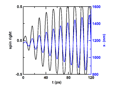
We start from the electron wavefunction with spin oriented along the -axis, i.e. an equally weighted linear combination of spin up and down components, generated as the ground state of the parabolic confinement potential. We perform simulations with a correctly tuned voltage oscillation frequency (in Eq. 21). As a result, we get expectation values of spin in the right half of the nanodevice (black curve) similar to the time courses from Fig. 7. The curve reaches the value , which indicates almost full spatial spin separation. The long plateau regions with mean that the intervals in which the spin remains separated are long enough to set an additional potential barrier between the separated spin density parts to further enhance separation.
The period of oscillations of voltages applied to the gates of the order of ps is near the limits of current technological capabilities. However, we should note that the frequency of oscillations depends on the parabolic confinement potential and can be reduced several times by lowering the control voltages by reducing the coefficient.
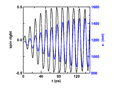
In Fig. 13, we can see another case of such simulations, but this time with the self-focusing effect included. The Poisson’s equation is solved with the same permittivity () for the entire computational box. This corresponds to a hypothetical situation in which the nanostructure is covered not with a dielectric layer but with a semiconductor layer of permittivity similar to the . This time the wavefunctions with opposite spins do not fully separate and does not reach the value of (or ) closely enough. The Poisson’s equation solution includes the self-focusing effect caused by the induced charge in both, the gates and the conducting substrate. The sources of this charge have an influence on the potential felt by the electron.
Let us look at Fig. 14.
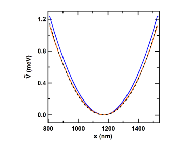
It presents how the potential energy in the QW changes with the inclusion of the self-focusing effect. The case with self-focusing (blue curve) clearly deviates from the case without self-focusing (red curve). The potential energy for the first case (blue curve) remains acceptably parabolical, but during wavefunction separation, the interaction with the induced charge weakens, since the wavepacket splits into two separated parts and the potential felt by each one changes. These changes and the resulting non-parabolicity hinder the electron acceleration. The effect of self-focusing could be mitigated by increasing the distance between the QW and the gates or the substrate.
III.3 Effect of adding a dielectric
In the proposed nanostructure (Fig. 10), the distance between the QW and the substrate is nm and for the top metallic gate nm, which are high enough for negligible self-focusing. However, to neutralize the influence of self-focusing originating from the rails and the side gates, we employ another nanodevice design. This is achieved by placing a dielectric layer on top of these gates—see Fig. 10 (but under the top gate), with permittivity lower than the permittivity of the QW material. For this purpose, we used material with permittivity (). If we simply used the image charge method for the interface of two dielectric media, the image charge induced within the material of lower permittivity would have the same (negative) sign as the primary charge (located in the material of higher permittivity). Therefore, such a dielectric addition could compensate the (positive) charge induced on the metallic gates.
We observe such an effect in simulations. In Fig. 14, the black dashed curve shows the potential energy calculated for one such case of compensation. In the device region between nm and nm in which the electron is accelerated and separated ( oscillations range—see: Fig. 13), the black curve from Fig. 14 coincides with the red one. This clearly means that self-focusing has been neutralized by defocussing due to the presence of the dielectric layer. Such a compensation also requires a careful tuning of the rail widths and the distance between them. Fig. 11 shows relatively large areas not covered with any gates. In these areas the semiconductor comes into direct contact with the dielectric.
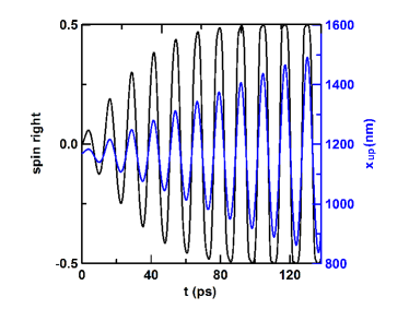
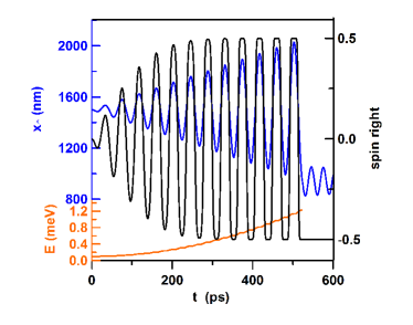
Fig. 15 shows results of the simulation with spin-dependent electron acceleration due to oscillating spin-orbit coupling in the nanostructure covered with the dielectric layer. This time the tuned voltage oscillation frequency is of . The course of the expectation value of the spin right starts to resemble ones from Figs. 7 and 12. Characteristic plateaus appear again, giving a lot of time for setting up a potential barrier between the separated parts. The most favorable moment to create such a barrier is at ps. At this moment we stop any oscillations of voltages and keep them fixed. Moreover, for the two gates marked as the voltages are decreased by mV, namely mV. This procedure elevates the potential in the center of the structure, creating a potential barrier. This effectively divides the nanodevice into two regions: left and right.
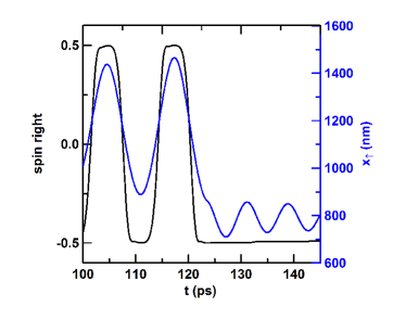
The last fragment of the simulation depicting the barrier setup moment is shown in Fig. 16. The (black curve) remains close to the value , which means that spin in the right part of the nanodevice is oriented down. The spin up position (blue curve) no longer returns to the upper part of the graph but it falls and remains down due to the repulsive influence of the barrier.
Now, the starts to oscillate in the left half of the nanodevice. These oscillations indicate that, during the separation stage, the electron did not get rid of the excess of energy. The frequency of the oscillations has also changed, since the local curvature of the confinement potential is now slightly different. The oscillations have a negative influence on the nanodevice operation, because the separated spin density part can tunnel through the barrier while colliding with it. This manifests itself via a small rise in the final part of the course (barely visible in Fig. 16).
Oscillations, however, can be easily eliminated by subsequent elevation of the barrier at the moment when the velocity of spin density parts (i.e. and ) is zero. Fig. 16 shows a good candidate for such a moment at ps. The barrier is elevated by decreasing the voltage applied to the gate by additional mV (now mV). Fig. 17 shows results of a simulation for that case, with no rise in the final part of the .
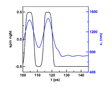
Fig. 18 shows the wavepacket and the potential barrier in the nanodevice center at the moment of maximal separation. This time we compare the spin and total electron densities calculated along the -axis but, unlike the 1D case, here also integrated along the direction. We use the following formulae:
| (22) |
| (23) |
The potential energy has two minima with a barrier between them. Both parts of the spin density are separated and oscillate closely around these minima, but the amplitude of oscillation is much smaller than in the case in which the potential barrier was elevated only once. If we raise a barrier of full height at the first time by lowering the voltages by the full mV at time , the amplitude of the oscillations will be significantly higher.
We mention that our proposal is robust against decoherence effects. The presented operation times on the electron spin are about ps for the complete electron spin density separation—see e.g. Figs. 12 or 15, and are much shorter than the electron spin coherence times in InSb material.van den Berg et al. (2013) These operation times might be further improved (reduced) by increasing the frequency .
Detection of the obtained Schrödinger’s cat states could be based on measuring a fraction of charge of a definite spin, so called spin-to-charge conversion, using a quantum point contact (QPC) interface.
IV Summary
We proposed a design for a nanodevice based on a typical planar semiconductor heterostructure in which it is possible to create an entangled state of Schrödinger’s cat type. This is achieved by spatial separation of the electron densities corresponding to opposite spin directions. Such a state has been generated in quantum optics Monroe et al. (1996); Leibfried et al. (2003); Myatt et al. (2000).
To create this state in our nanostructure, we need to use coherent states of the harmonic oscillator which are obtainable only for ideally parabolic confinement potentials. Generation of such a potential is one of the most important results of this paper. Nearly ideal parabolic potential along the -axis is achievable in the proposed multi-gate nanodevice (see: Figs. 10 and 11) if we neglect the interaction of the electron confined in the quantum well with the induced charge on the device gates. This interaction causes self-focusing of the electron density, making spin separation much harder. A remedy for this effect is defocussing achieved by covering the entire nanostructure with a dielectric of lower permittivity compared to the well material. We have shown that self-focusing can be effectively compensated by adding a dielectric layer with simultaneous careful adjustment of the inner gate (rails) geometry.
We have performed simulations of numerous variants of our nanodevice via solution of the time-dependent Schrödinger equation with simultaneous tracking of the potential via solution of the Poisson’s equation at every time step. As a result, we were able to take into account the geometry details, varying voltages applied to gates and changes of the electron density. Including also oscillating spin-orbit interaction, which induces the spin separation effect.
Acknowledgements.
This work has been supported by National Science Centre, Poland, under UMO-2014/13/B/ST3/04526.*
Appendix A The Rashba spin-orbit coupling in semiconductor heterostructures
Here we will briefly review valid models of the Rashba effect in III-V asymmetric semiconductor heterostructures. We will make calculations of the spin-orbit coupling for these models, and compare them showing the validity of our chosen model (Eq. 20).
Starting with the earliest works of Bychkov and RashbaBychkov and Rashba (1984a, b), where they introduce discussed models, electrons confined at the heterojunction form two-dimensional electron gas (with and degrees of freedom):
| (24) |
with two-dimensional electron momentum , and versor normal to the junction surface. The coupling strength in the Hamiltonian (24) is proportional to the external electric field (introducing asymmetry to the confinement) and some material dependent parameter , which describes material details of the junction in -direction: . Moreover in [Winkler, 2003] we find a summary of the famous discussion between AndoAndo et al. (1982) and LassnigLassnig (1985), which states that the Rashba spin-coupling in the conduction band results from the electric field in the valence band: .
In work [de Andrada e Silva et al., 1994] the authors skip the band offset at the junction assuming an infinite barrier. Therefore, when calculating the , they take the parameters of the conduction and valence bands only for the well material, using formula:
| (25) |
For the InSb band parametersVurgaftman et al. (2001) meV, meV, we get from above formula . A more complicated than (25) but also a more accurate formula [Winkler, 2003, Eq. 6.22] gives a similar value . The coupling is proportional to the external field , which in general is three-dimensional [Winkler, 2003, Eq. 6.9]. In this work we assume a similar model, by replacing in (Eq. 24), thus obtaining (Eq. 20), and taking the parameter value of .
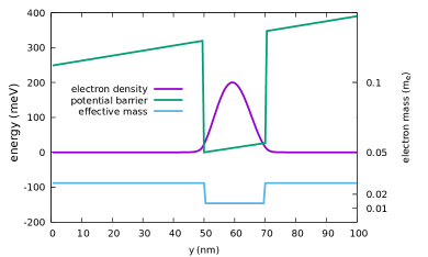
Let us now see if our modelde Andrada e Silva et al. (1994); Winkler (2003) is sufficient and compare it with the model presented in [Toloza Sandoval et al., 2011]. The latter is a refinement of [de Andrada e Silva et al., 1994] and is complete in sense, that it contains the confinement details within the heterostructure quantum well in the growth direction ()—including different material parameters on both sides of the junction (effective masses, coupling values and bands parameters). Now we assume a single electron confined in the direction within our heterostructure, i.e. in a nm width /InSb/ quantum well (with ) and the conduction band offset meV together with the external field . Such a conduction band profile for the heterostructure used in our device is shown in Fig. 19 (green curve).
Let us now assume the effective Hamiltonian in the -direction for a conduction electronToloza Sandoval et al. (2011) (nonparabolicity is negligible here) as:
| (26) |
Note that the effective mass is discontinuous here, with the value of for the InSb well, and outside in the barriers region. The band mass in heterostructure is denoted by the blue curve in Fig. 19.
For AlSb band mass is equal ,Vurgaftman et al. (2001) thus for the barrier alloy we assume . Similarly, for the AlSb material we get meV, meV and, resulting from (Eq. 25), the spin orbit coupling . The band mass and the spin-orbit coupling should be further renormalized in the barrier region. Using formulas [Eqs. 7 and 9 from Toloza Sandoval et al., 2011] we finally obtain and .
For these parameters we find eigenstates of the Hamiltonian (Eq. 26). We assume that the electron confined in the junction is in the ground state . For such a narrow quantum well ( nm) the 1st excited state is separated on the energy scale by about 120 meV. In a quantum well of height of 320 meV and width of 20 nm we have 3 bound states of energies: meV, meV and meV. For this calculated conduction electron density (magenta in Fig. 19) we can finaly calculate the average value of the Rashba coupling in the heterostructure:
| (27) |
Note that the depends on the external electric field via the Hamiltonian (26).
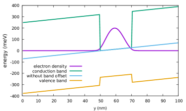
For comparison, we additionally calculate the RSOI coupling value in our heterostructure within the simple toy model .Winkler (2003) The coupling is here simply calculated as product of the (in InSb) and the average electric field within the valence band (orange curve in Fig. 20) weighted with the electron density (magenta curve) in the conduction band (green curve): . For a given the effective coupling equals . The electron density is calculated here as in Fig. 19. We compare this result with the analytical expression for [Eq. 6.33 from Winkler, 2003], with the offset in the valence band ,Vurgaftman et al. (2001) giving .
Let us now compare all the presented models as a function of the external electric field assuming values, as in our nanodevice, between and mV/nm. In Fig. 21 we plotted for: the most accurate model Toloza Sandoval et al. (2011), taking into account confinement details in direction as well as the barrier material (green curve); the simple toy model calculating a mean field in the valence band Winkler (2003) (blue curve). Both are compared with from a model that neglects details about the barrier in the junctionWinkler (2003); de Andrada e Silva et al. (1994) (magenta) and the analytic solution from a toy modelWinkler (2003) . Last two curves are independent of the electric field . Values for the toy model (blue and orange) slightly overestimate the value we assumed (magenta). Nevertheless the most accurate and complex model (green) produces results that are about 1% lower for the range of electric fields used in our device (not greater than about ).
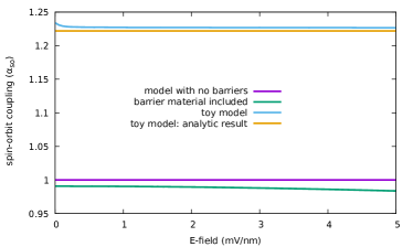
According to presented calculations we conclude that within the range of electric fields present in our device, corrections to taking into account details of confinement in the junction are negligible (of the order of 1%). Thus in our calculations we use a simpler spin-orbit coupling model, which takes into account only the QW material, for which we get the coupling constant .
References
- Hanson et al. (2007) R. Hanson, L. P. Kouwenhoven, J. R. Petta, S. Tarucha, and L. M. K. Vandersypen, Rev. Mod. Phys. 79, 1217 (2007).
- Žutić et al. (2004) I. Žutić, J. Fabian, and S. Das Sarma, Rev. Mod. Phys. 76, 323 (2004).
- Ladd et al. (2010) T. D. Ladd, F. Jelezko, R. Laflamme, Y. Nakamura, C. Monroe, and J. L. O’Brien, Nature 464, 45 (2010).
- Hasan and Kane (2010) M. Z. Hasan and C. L. Kane, Rev. Mod. Phys. 82, 3045 (2010).
- Zhang and Nori (2015) P. Zhang and F. Nori, Phys. Rev. B 92, 115303 (2015).
- Fu and Kane (2008) L. Fu and C. L. Kane, Phys. Rev. Lett. 100, 096407 (2008).
- Lutchyn et al. (2010) R. M. Lutchyn, J. D. Sau, and S. Das Sarma, Phys. Rev. Lett. 105, 077001 (2010).
- Klinovaja et al. (2012) J. Klinovaja, P. Stano, and D. Loss, Phys. Rev. Lett. 109, 236801 (2012).
- Oreg et al. (2010) Y. Oreg, G. Refael, and F. von Oppen, Phys. Rev. Lett. 105, 177002 (2010).
- Owen et al. (2014) E. T. Owen, M. C. Dean, and C. H. W. Barnes, Phys. Rev. A 89, 032305 (2014).
- Bertoni et al. (2000) A. Bertoni, P. Bordone, R. Brunetti, C. Jacoboni, and S. Reggiani, Phys. Rev. Lett. 84, 5912 (2000).
- Hayashi et al. (2003) T. Hayashi, T. Fujisawa, H. D. Cheong, Y. H. Jeong, and Y. Hirayama, Phys. Rev. Lett. 91, 226804 (2003).
- Petersson et al. (2010) K. D. Petersson, J. R. Petta, H. Lu, and A. C. Gossard, Phys. Rev. Lett. 105, 246804 (2010).
- Loss and DiVincenzo (1998) D. Loss and D. P. DiVincenzo, Phys. Rev. A 57, 120 (1998).
- Kloeffel and Loss (2013) C. Kloeffel and D. Loss, Annu. Rev. Condens. Matter Phys. 4, 51 (2013).
- Shulman et al. (2012) M. D. Shulman, O. E. Dial, S. P. Harvey, H. Bluhm, V. Umansky, and A. Yacoby, Science 336, 202 (2012).
- Trifunovic et al. (2012) L. Trifunovic, O. Dial, M. Trif, J. R. Wootton, R. Abebe, A. Yacoby, and D. Loss, Phys. Rev. X 2, 011006 (2012).
- Trifunovic et al. (2013) L. Trifunovic, F. L. Pedrocchi, and D. Loss, Phys. Rev. X 3, 041023 (2013).
- Pal et al. (2015) A. Pal, E. I. Rashba, and B. I. Halperin, Phys. Rev. B 92, 125409 (2015).
- Mehl and DiVincenzo (2015) S. Mehl and D. P. DiVincenzo, Phys. Rev. B 92, 115448 (2015).
- Hassler et al. (2015) F. Hassler, G. Catelani, and H. Bluhm, Phys. Rev. B 92, 235401 (2015).
- Szumniak et al. (2015) P. Szumniak, J. Pawłowski, S. Bednarek, and D. Loss, Phys. Rev. B 92, 035403 (2015).
- Bednarek et al. (2008a) S. Bednarek, B. Szafran, R. J. Dudek, and K. Lis, Phys. Rev. Lett. 100, 126805 (2008a).
- Bednarek and Szafran (2009) S. Bednarek and B. Szafran, Nanotechnology 20, 065402 (2009).
- Bednarek et al. (2010) S. Bednarek, P. Szumniak, and B. Szafran, Phys. Rev. B 82, 235319 (2010).
- Bednarek and Szafran (2008) S. Bednarek and B. Szafran, Phys. Rev. Lett. 101, 216805 (2008).
- Rashba (1960) E. Rashba, Sov. Phys. Solid State 2, 1109 (1960).
- Bychkov and Rashba (1984a) Y. A. Bychkov and E. Rashba, JETP lett 39, 78 (1984a).
- Bychkov and Rashba (1984b) Y. A. Bychkov and E. I. Rashba, Journal of Physics C: Solid State Physics 17, 6039 (1984b).
- Winkler (2003) R. Winkler, Spin-orbit Coupling Effects in Two-Dimensional Electron and Hole Systems (Springer-Verlag Berlin Heidelberg, 2003).
- Nowack et al. (2007) K. C. Nowack, F. H. L. Koppens, Y. V. Nazarov, and L. M. K. Vandersypen, Science 318, 1430 (2007).
- Nadj-Perge et al. (2010) S. Nadj-Perge, S. Frolov, E. Bakkers, and L. P. Kouwenhoven, Nature 468, 1084 (2010).
- Nadj-Perge et al. (2012) S. Nadj-Perge, V. S. Pribiag, J. W. G. van den Berg, K. Zuo, S. R. Plissard, E. P. A. M. Bakkers, S. M. Frolov, and L. P. Kouwenhoven, Phys. Rev. Lett. 108, 166801 (2012).
- Malard et al. (2011) M. Malard, I. Grusha, G. I. Japaridze, and H. Johannesson, Phys. Rev. B 84, 075466 (2011).
- López et al. (2012) A. López, Z. Z. Sun, and J. Schliemann, Phys. Rev. B 85, 205428 (2012).
- Ban et al. (2012) Y. Ban, X. Chen, E. Y. Sherman, and J. G. Muga, Phys. Rev. Lett. 109, 206602 (2012).
- Čadež et al. (2014) T. Čadež, J. H. Jefferson, and A. Ramšak, Phys. Rev. Lett. 112, 150402 (2014).
- Szaszkó-Bogár et al. (2015) V. Szaszkó-Bogár, F. M. Peeters, and P. Földi, Phys. Rev. B 91, 235311 (2015).
- Pawłowski et al. (2016a) J. Pawłowski, P. Szumniak, and S. Bednarek, Phys. Rev. B 93, 045309 (2016a).
- Pawłowski et al. (2014) J. Pawłowski, P. Szumniak, A. Skubis, and S. Bednarek, Journal of Physics: Condensed Matter 26, 345302 (2014).
- Wineland (2013) D. J. Wineland, Rev. Mod. Phys. 85, 1103 (2013).
- Lau et al. (2014) H. W. Lau, Z. Dutton, T. Wang, and C. Simon, Phys. Rev. Lett. 113, 090401 (2014).
- Ralph et al. (2003) T. C. Ralph, A. Gilchrist, G. J. Milburn, W. J. Munro, and S. Glancy, Phys. Rev. A 68, 042319 (2003).
- Liao et al. (2016) J.-Q. Liao, J.-F. Huang, and L. Tian, Phys. Rev. A 93, 033853 (2016).
- Monroe et al. (1996) C. Monroe, D. M. Meekhof, B. E. King, and D. J. Wineland, Science 272, 1131 (1996).
- Leibfried et al. (2003) D. Leibfried, R. Blatt, C. Monroe, and D. Wineland, Rev. Mod. Phys. 75, 281 (2003).
- Myatt et al. (2000) C. J. Myatt, B. E. King, Q. A. Turchette, C. A. Sackett, D. Kielpinski, W. M. Itano, C. Monroe, and D. J. Wineland, Nature 403, 269 (2000).
- Sackett et al. (2000) C. Sackett, D. Kielpinski, B. King, C. Langer, V. Meyer, C. Myatt, M. Rowe, Q. Turchette, W. Itano, D. Wineland, et al., Nature 404, 256 (2000).
- Jeong and Kim (2002) H. Jeong and M. S. Kim, Phys. Rev. A 65, 042305 (2002).
- Owen et al. (2012) E. T. Owen, M. C. Dean, and C. H. W. Barnes, Phys. Rev. A 85, 022319 (2012).
- Pyshkin et al. (2016) P. V. Pyshkin, E. Y. Sherman, D.-W. Luo, J. Q. You, and L.-A. Wu, Phys. Rev. B 94, 134313 (2016).
- Kataoka et al. (2009) M. Kataoka, M. R. Astley, A. L. Thorn, D. K. L. Oi, C. H. W. Barnes, C. J. B. Ford, D. Anderson, G. A. C. Jones, I. Farrer, D. A. Ritchie, and M. Pepper, Phys. Rev. Lett. 102, 156801 (2009).
- Pawłowski et al. (2016b) J. Pawłowski, P. Szumniak, and S. Bednarek, Phys. Rev. B 94, 155407 (2016b).
- Blatt and Wineland (2008) R. Blatt and D. Wineland, Nature 453, 1008 (2008).
- McDonnell et al. (2007) M. J. McDonnell, J. P. Home, D. M. Lucas, G. Imreh, B. C. Keitch, D. J. Szwer, N. R. Thomas, S. C. Webster, D. N. Stacey, and A. M. Steane, Phys. Rev. Lett. 98, 063603 (2007).
- Bednarek et al. (2005) S. Bednarek, B. Szafran, and K. Lis, Phys. Rev. B 72, 075319 (2005).
- Bednarek and Szafran (2006) S. Bednarek and B. Szafran, Phys. Rev. B 73, 155318 (2006).
- Szumniak et al. (2012) P. Szumniak, S. Bednarek, B. Partoens, and F. M. Peeters, Phys. Rev. Lett. 109, 107201 (2012).
- Bednarek et al. (2008b) S. Bednarek, K. Lis, and B. Szafran, Phys. Rev. B 77, 115320 (2008b).
- Turchette et al. (2000) Q. A. Turchette, C. J. Myatt, B. E. King, C. A. Sackett, D. Kielpinski, W. M. Itano, C. Monroe, and D. J. Wineland, Phys. Rev. A 62, 053807 (2000).
- Dai et al. (2000) N. Dai, G. A. Khodaparast, F. Brown, R. E. Doezema, S. J. Chung, and M. B. Santos, Applied Physics Letters 76, 3905 (2000).
- Dai et al. (1998) N. Dai, F. Brown, R. E. Doezema, S. J. Chung, K. J. Goldammer, and M. B. Santos, Applied Physics Letters 73, 3132 (1998).
- Gouider et al. (2010) F. Gouider, Y. B. Vasilyev, M. Bugár, J. Könemann, P. D. Buckle, and G. Nachtwei, Phys. Rev. B 81, 155304 (2010).
- Zajac et al. (2016) D. M. Zajac, T. M. Hazard, X. Mi, E. Nielsen, and J. R. Petta, Phys. Rev. Applied 6, 054013 (2016).
- Granger et al. (2015) G. Granger, G. C. Aers, S. A. Studenikin, A. Kam, P. Zawadzki, Z. R. Wasilewski, and A. S. Sachrajda, Phys. Rev. B 91, 115309 (2015).
- Ward et al. (2016) D. R. Ward, D. Kim, D. E. Savage, M. G. Lagally, R. H. Foote, M. Friesen, S. N. Coppersmith, and M. A. Eriksson, Npj Quantum Information 2, 16032 EP (2016), article.
- Dresselhaus (1955) G. Dresselhaus, Phys. Rev. 100, 580 (1955).
- Studer et al. (2010) M. Studer, M. P. Walser, S. Baer, H. Rusterholz, S. Schön, D. Schuh, W. Wegscheider, K. Ensslin, and G. Salis, Phys. Rev. B 82, 235320 (2010).
- Ye et al. (2012) H. Q. Ye, G. Wang, B. L. Liu, Z. W. Shi, W. X. Wang, C. Fontaine, A. Balocchi, T. Amand, D. Lagarde, P. Renucci, and X. Marie, Applied Physics Letters 101, 032104 (2012).
- Davies et al. (1980) K. Davies, H. Flocard, S. Krieger, and M. Weiss, Nuclear Physics A 342, 111 (1980).
- van den Berg et al. (2013) J. W. G. van den Berg, S. Nadj-Perge, V. S. Pribiag, S. R. Plissard, E. P. A. M. Bakkers, S. M. Frolov, and L. P. Kouwenhoven, Phys. Rev. Lett. 110, 066806 (2013).
- Ando et al. (1982) T. Ando, A. B. Fowler, and F. Stern, Rev. Mod. Phys. 54, 437 (1982).
- Lassnig (1985) R. Lassnig, Phys. Rev. B 31, 8076 (1985).
- de Andrada e Silva et al. (1994) E. A. de Andrada e Silva, G. C. La Rocca, and F. Bassani, Phys. Rev. B 50, 8523 (1994).
- Vurgaftman et al. (2001) I. Vurgaftman, J. R. Meyer, and L. R. Ram-Mohan, Journal of Applied Physics 89, 5815 (2001), http://dx.doi.org/10.1063/1.1368156 .
- Toloza Sandoval et al. (2011) M. A. Toloza Sandoval, A. Ferreira da Silva, E. A. de Andrada e Silva, and G. C. La Rocca, Phys. Rev. B 83, 235315 (2011).