Magnetic gap opening in rhombohedral-stacked multilayer graphene from first principles
Abstract
We investigate the occurrence of magnetic and charge density wave instabilities in rhombohedral-stacked multilayer (three to eight layers) graphene by first principles calculations including exact exchange. Neglecting spin-polarization, an extremely flat surface band centered at the special point of the Brillouin zone occurs at the Fermi level. Spin polarization opens a gap in the surface state by stabilizing an antiferromagnetic state. The top and the bottom surface layers are weakly ferrimagnetic in-plane (net magnetization smaller than ), and are antiferromagnetic coupled to each other. This coupling is propagated by the out-of-plane antiferromagnetic coupling between the nearest neighbors. The gap is very small in a spin-polarized generalized gradient approximation, while it is proportional to the amount of exact exchange in hybrid functionals. For trilayer rhombohedral graphene it is meV in PBE0, in agreement with the meV gap found in experiments. We study the temperature and doping dependence of the magnetic gap. At electron doping of cm-2 the gap closes. Charge density wave instabilities with periodicity do not occur.
In a solid, at low enough density, the Coulomb energy dominates the single particle energy and electronic instabilities such as magnetic phases or even Wigner crystallization become possible. A reduction of the single-particle energy, and a consequent enhancement of the electron-electron interaction, can be obtained by considering a metallic system with a very flat single-particle band-dispersion. This unfortunately does not happen in graphene where the high Fermi velocity prevents electronic instability. The situation is different, however, in weakly doped Bernal-stacked (AB) even-multilayer graphene (see Fig. 1), as the single-particle bands become massive. Indeed, a spontaneously gapped ground state is already observed in suspended bilayer Freitag et al. (2012); Jr et al. (2012) and four-layer graphene (1.5 meV gap)Grushina et al. (2015).
Even more favorable to electronic instabilities is rhombohedral-stacked (ABC) multilayer graphene. Neglecting spin polarization, tight-binding and density functional theory (DFT) calculations find bulk rhombohedral graphite to be metallic with a high Fermi velocity (see grey region in Fig. 1). On the contrary, within these approximations, rhombohedral-stacked multilayer graphene (RSMG) displays the occurrence of an extremely flat surface state at the Fermi level (see Fig. 1) located at the point of the graphene Brillouin zone (BZ) Koshino (2013); Jung and MacDonald (2013); Latil and Henrard (2006); Xiao et al. (2011); Wu (2011); Otani et al. (2010). The extension of the surface state in the BZ increases with increasing thickness and saturates at layers. Its bandwidth is at most meV for flakes of fewer than eight layers. The extremely reduced bandwidth makes RSMG one of the strongest correlated systems known nowadays and an ideal candidate for correlated states even in the absence of orbitals.
On the experimental side, only recently has it been possible to synthesize RSMG. Ouerghi et al. Pierucci et al. (2015) found five-layer RSMG on top of a cubic SiC substrate to be metallic with a very high density of states at the Fermi level, in agreement with spinless DFT predictions. More recent work on suspended ABC trilayer Lee et al. (2014) seems to suggest that a gap as large as meV occurs at the Fermi level. However, in transport measurements with singly gated devices, where the charge density and the potential difference cannot be controlled independently, the gap is much smaller Bao et al. (2011). The origin of this gap state has been suggested to be related to a magnetic state in which the external layers are antiferromagnetic coupled while the in-plane spin state is ferrimagnetic Lee et al. (2014); Throckmorton and Vafek (2012). Finally, it is worth mentioning that it has been claimed that RSMG flakes composed of 17 layers can be isolated from kish graphite Henni et al. (2016). However it is still unknown if a gap opens in these samples.

In this work, by using density functional theory calculations with several hybrid functionals we investigate the occurrence of charge and magnetic instabilities in RSMG. We also discuss the effect of doping and temperature on the interaction induced gap.
DFT calculations are performed using the CRYSTAL code Dovesi et al. (2014) with the triple--polarized Gaussian type basis sets for the C atoms Peintinger et al. (2013). The PBE0 Adamo and Barone (1999) and other hybrid functionals with several degrees of exact exchange (see Appendix A) have been used for DFT calculations. The band flatness and the extreme localization of the low energy states around the special point require an ultradense sampling with an electronic k mesh of . We used real space integration tolerances of 7-7-7-15-30, and with an energy tolerance of Ha for the total energy convergence. Fermi-Dirac smearing for the occupation of the electronic states is used for all of the calculations. The density of states is obtained with a Gaussian smearing of 0.00005 Ha. In the magnetic case, we fix the magnetic state in the first iteration of the self-consistent cycle and then we release the constraint. We choose an in-plane lattice parameter of Å, and an inter-plane distance of 3.347 Å. A vacuum of 10.04 Å is placed between the periodic images along the direction.
We consider , being the number of layers. We start the simulation from an initial magnetic state having ferromagnetic coupling in the surface layers and antiferromagnetic coupling between them. In both spin polarized PBE Perdew et al. (1996) and exact exchange functionals (HSE06, PBE0, etc.), we always converge to a magnetic state that is (1) globally, an antiferromagnetic spin state, namely for each spin up band we have a spin down band degenerate in energy but localized on different atoms; (2) ferrimagnetic within the surface layers where the two atoms have opposite spins with slightly different magnetic moment; and (3) with antiferromagnetic coupling between the top and bottom layers. The magnitude of the spin drops significantly farther away from the surface. This magnetic state is similar to the one found in bilayer and trilayer graphene in the framework of Hubbard-like models Lee et al. (2014); Throckmorton and Vafek (2012) (the so-called layered antiferromagnetic state); however, here the module of the magnetic moments in each outer surface layer is identical up to 0.001 , meaning that we are much closer to an in-plane antiferromagnetic state than a ferrimagnetic state.
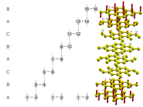
Figure 2 shows a schematic diagram of rhombohedral graphene, with arrows representing the direction of the spin for all layers up to eight layers. In rhombohedral graphene, the total number of atoms is , with each layer having two covalent bonded C atoms, only one of which is weakly bonded to the neighboring layer. The labeling of the atoms starts from the bottom layer, where atom 1 is covalent bonded to atom 2, and atom 2 is weakly bonded to atom 3 of the next layer, and the labeling follows the covalent to weak interlayer bond. The magnetic order we find is such that the odd-numbered atoms have down spin, and the even numbered atoms have up spin, with the spin magnetic moments such that . The outermost surface layers are ferrimagnetic with . In-plane and out-of-plane nearest neighbors are antiferromagnetic coupled.
Within spin-polarized PBE, the local magnetic moments are essentially zero. The increase of the exact exchange component in the functional enhances the magnetic moments. The magnetic moments in the outermost layers are larger for eight-layer thick flakes and within PBE0 they are as large as bohr magnetons in magnitude (see Table 1). The magnetic moments for other functionals are shown in Appendix A.
| N | ||||||||
|---|---|---|---|---|---|---|---|---|
| 3 | -5.28 | 4.60 | -2.73 | |||||
| 4 | -7.32 | 6.33 | -3.22 | 3.11 | ||||
| 5 | -8.56 | 7.38 | -3.62 | 3.43 | -2.60 | |||
| 6 | -9.19 | 7.90 | -3.82 | 3.58 | -2.34 | 2.29 | ||
| 7 | -9.75 | 8.40 | -4.11 | 3.84 | -2.38 | 2.30 | -1.93 | |
| 8 | -10.04 | 8.64 | -4.23 | 3.94 | -2.34 | 2.24 | -1.69 | 1.66 |
The PBE0 magnetic electronic structure for is shown in Fig. 3. Each band is doubly degenerate with spin up and down states having the same energy. Therefore globally the system is in an antiferromagnetic state. This magnetic order results in a gapped state, with the gap at the K point increasing with . The surface bands are quite flat with a small asymmetry between the and directions that increases with . This behavior is easily understood as for the surface projected bulk bands of rhombohedral graphite should be recovered (see Fig. 1). More insight into the gap opening at is obtained by analyzing the projected electronic bands on the atoms of the surface layers. The surface states are dominated by the orbitals of two C atoms. On each surface layer, only the atom having no out-of-plane neighboring atoms contributes to the surface bands (see Appendix B). For comparison, the electronic structure of metallic and paramagnetic state is given Appendix C.

We find the band gap for rhombohedral trilayer graphene to be meV with the PBE0 functional. This result is in good agreement with the experimentally reported value of meV in Ref. Lee et al. (2014). By using other functionals with different percentages of exact exchange and range separation we find smaller gaps as shown in Appendix A. As the PBE0 gap gives the best agreement with experiment we use this functional for the rest of the paper.
The change in the band gap at zero temperature for different layers is shown in Figs. 3 and 4 and Table 2. The band gap increases significantly from three to four layers, but saturates after five layers. At eight layers, the gap starts to close slowly, with increasing deviation from the flat bands, in order to reach the bulk limit Ho et al. (2016) shown in Fig. 1.

As the gap is strongly temperature dependent in experiments and closes at KLee et al. (2014), we study the antiferromagnetic gap as a function of temperature. This is done by including a Fermi-Dirac occupation of the electronic states. The temperature dependence of the gap is shown in Fig. 4. To obtain , we fit the band gap to the function,
| (1) | |||||
with the constants arranged such that the first and the second derivative of the curve is zero at the zero temperature limit. The temperature dependence of the band gap has a similar behavior to that obtained from the experiments in Ref. Lee et al. (2014). However, the thermal suppression of the gap is slower in our calculations, resulting in a larger K, as compared to the experimental value of K for trilayer graphene. We attribute the discrepancy between theory and experiments to the imperfect treatment of screening at the hybrid functional level.
Similarly to what happens for the layer dependence of the band gap with the number of layers, increases up to five layers, and then saturates and changes slowly. The values and the fit parameter of each layer are shown in Table 2 for different numbers of layers.
| N | (meV) | (K) | |
|---|---|---|---|
| 3 | 38.60 | 126.53 | 2.97 |
| 4 | 50.96 | 161.21 | 3.28 |
| 5 | 55.70 | 173.90 | 3.36 |
| 6 | 55.78 | 177.67 | 3.60 |
| 7 | 55.26 | 183.58 | 3.36 |
| 8 | 53.19 | 185.67 | 3.43 |
Contrary to the case of suspended samples, supported RSMG shows a metallic behavior Pierucci et al. (2015). A possible reason for this could be the presence of a substrate doping Lee et al. (2014). In order to verify this hypothesis, we consider n-doping of rhombohedral trilayer graphene. We use a compensating jellium background to enforce charge neutrality.
To estimate the number of electrons needed to close the gap, we have integrated the first peak of the density of states in Fig. 3. For the trilayer rhombohedral graphene an electron density of cm-2 (corresponding to electrons/cell) is needed to fill the flat conduction band region. This electron density increases to cm-2 for eight layers. The results for the rest of the layers are presented in Appendix D.
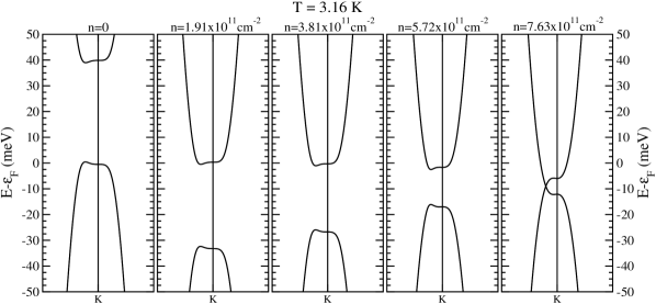
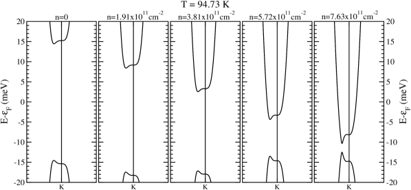
We find that doping reduces the band gap. In agreement with our estimation from the density of states, the gap ultimately closes at cm-2, to be compared to cm-2 found in experiments Lee et al. (2014). The combined effect of doping and temperature is shown in Fig. 5 (and in Appendix E). We conclude that substrate doping can be responsible of the differences between supported and suspended samples. We can also speculate that the critical doping to close the gap could grow by an order of magnitude by increasing the number of ABC stacked layers.

Up to now we consider the possibility of magnetic gap opening in RSMG. However, charge density wave instabilities could also open a gap via phonon softening. In order to validate this hypothesis, we calculate phonon frequencies at and by using the finite differences method and the spinless PBE0 functional in rhombohedral-stacked trilayer graphene. We find that the largest softening occurs at the K point of the Brillouin zone Lazzeri et al. (2008) for the in-plane phonon mode. Despite PBE0 substantially softens the phonon frequencies with respect to PBE, all the phonon modes are stable so that a structural distortion compatible with a periodicity is excluded. The magnitude of the phonon modes are also reported in Appendix F. Magnetism is then the most likely instability in RSMG.
In this paper, we have analyzed the magnetic and charge instabilities in rhombohedral stacked multilayer graphene using spin-polarized hybrid functionals. While in the absence of spin-polarization an extremely flat surface state occurs at the Fermi level, the introduction of spin polarization leads to magnetic instabilities and opening of a gap in the surface state. The state is such that the surface layers are weakly ferrimagnetic in-plane, and the top and the bottom layers are antiferromagnetic coupled, which is propagated by the out-of-plane antiferromagnetic coupling between the nearest neighboring atoms. The globally stable state is antiferromagnetic where the spin up and spin down bands are degenerate. Within PBE0 the gap is found to agree with experiments on ABC trilayer graphene. We have shown that doping suppress the gap, explaining the experimental finding that a gap occurs in trilayer ABC graphene only in suspended samples. Finally, we study the possible occurrence of charge density wave instabilities with supercell. We found that no charge density wave occurs so that the gap opening seen in experiments is only due to the magnetic coupling of the surface atoms in the multilayers. Our work demonstrate that the inclusion of exact exchange in first principles calculations and an ultradense sampling of the Brillouin zone are crucial in order to explain the magnetic and structural instabilities of rhombohedral-stacked multilayer graphene.
Acknowledgements.
This work is supported by the Graphene Flagship, and by Prace (Proposal number 2015133134). Calculations were performed at IDRIS, CINES, CEA and BSC TGCC.Appendix A Exchange and Correlation Functionals
To understand the effect of exchange and range separation in the hybrid functionals on the band gap of the system, we have tuned exchange components and range separation. The results are given in Fig. 6.
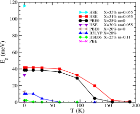
For the same range separation parameter, Å-1, the increasing percentage of exact exchange increases the band gap significantly. For the same percentage of exact exchange, increasing the range separation decreases the band gap, as can be seen when comparing the PBE0 functional to the HSE06 functional Krukau et al. (2006).
Only with PBE0 functional, we obtain a band gap similar to the experimental value.
When we change the exact exchange and range separation of the HSE functional such that the band gap is similar to that of PBE0 at zero temperature limit (X Å-1), we obtain a similar temperature dependence for both functionals.
With the B3LYP functional Vosko et al. (1980), we obtain a similar to the experimental value, however the calculated band gap at zero temperature is too small compared to the experimental result Lee et al. (2014).
| XC | X | ||||
|---|---|---|---|---|---|
| PBE | 0 | 0 | -0.0001 | 0.0001 | -0.0002 |
| HSE06 | 25 | 0.11 | -0.4589 | 0.3581 | -0.1282 |
| B3LYP | 20 | 0 | -1.4442 | 1.1316 | -0.5043 |
| PBE0 | 20 | 0 | -1.8892 | 1.5258 | -0.7099 |
| HSE | 30 | 0.055 | -5.2116 | 4.5689 | -2.6368 |
| PBE0 | 25 | 0 | -5.2831 | 4.5951 | -2.7317 |
| HSE | 31 | 0.055 | -6.5798 | 5.8432 | -3.5352 |
| HSE | 35 | 0.055 | -17.5428 | 16.2741 | -12.3476 |
The value of the band gap is directly linked to the magnitude of the spin in the surface atoms, which can be seen in Table 3. The PBE functional predicts a spinless paramagnetic state, while the introduction of the exact exchange immediately stabilizes the magnetic state. With the increase of the amount of exact exchange the magnitude of the spin on the surface atoms increases, and with the increase of the range separation the magnitude of the spin of the surface atoms decreases.
Appendix B Projected Band Structure
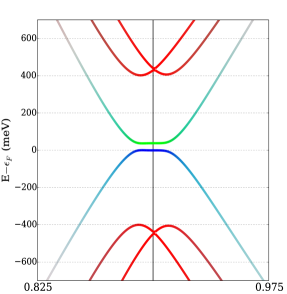
In Fig. 7, we present the electronic band structure projected onto the spin-down state of orbital. The flat bands are dominated by atom 1 (blue in the figure) and 6 (green), for the spin down bands. These are one of the atoms on each surface, and are antiferromagnetic coupled. The other atom of each surface, i.e., atoms 2 and 5 (red), contribute only to the bulk bands. The spin-up figure would look exactly the same except now blue would be atom 6 and green would be atom 1.
In order to understand the interplay between in-plane and out-of-plane magnetic couplings in determining the gap structure we performed, for three and four layers, a calculation starting from an in-plane antiferromagnetic spin order and an out-of-plane ferromagnetic order. The self-consistent cycle preserves this magnetic state; however, the resulting band structure is gapless. This reveals that the inter-layer antiferromagnetic coupling plays a crucial role in the gap opening in three- and four-layer rhombohedral graphene.
Appendix C Metallic and Paramagnetic Bands
In Fig. 8, we present the electronic band structure and the density of states of the paramagnetic state calculated with the PBE0 functional between three and eight layers.
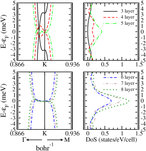
The paramagnetic electronic band calculations are performed with the same parameters as the magnetic calculations, except the initial conditions on the spin of each atom are not set and Fermi-Dirac smearing of 0.00001 Ha is used. The density of states is calculated with a Gaussian smearing of 0.00004 Ha.
The crossing points of the bands in our paramagnetic calculations are comparable to the previous results obtained for three and four layers with standard DFT calculations Latil and Henrard (2006).
As compared to the bulk bands of rhombohedral graphite with DFT Wong et al. (2011); Charlier et al. (1994); Chiu et al. (2011); Xiao et al. (2011) and tight binding Chiu et al. (2011) calculations, and to the evolution of graphene to graphite with tight binding calculation Ho et al. (2016), it is clear that these states are surface states of the few-layer rhombohedral graphene.
Appendix D Electrons on the Flat Surface Bands
In order to understand the amount of charge needed to fill the flat surface band and close the gap, we have integrated first peak of the density of states above the gap. The results for each layer are shown in Table 4.
| N | ||
|---|---|---|
| 3 | 0.00042 | 8.01 |
| 4 | 0.00116 | 22.12 |
| 5 | 0.00209 | 39.86 |
| 6 | 0.00268 | 47.30 |
| 7 | 0.00326 | 62.17 |
| 8 | 0.00355 | 67.70 |
For the trilayer rhombohedral graphene, a doping of electrons/cell is needed to fill the flat conduction band, and this is in agreement with our calculations that at electrons/cell the band gap closes, as will be discussed in the following Appendix. Note that the width of the flat region decreases with increasing doping.
Appendix E Band Gap with Changing Temperature and Doping
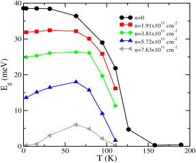
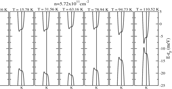
To understand the effect of the doping on the band gap, we introduced electrons/cell (corresponding to the electron density of cm-2) to the trilayer rhombohedral graphene. In Fig. 9, we present the temperature dependence of the band gap for different doping, as compared to the undoped case.
With the increasing temperature, after K the band gap decreases sharply, as expected. However, at low temperatures, the band gap first increases. In Fig. 10, we present the electronic structure at doping cm-2 for different temperatures. In addition, to understand the correlation between the increase in the gap and the spins, we present the spins of each atom at different temperatures for this doping in Table 5.
| T (K) | |||
|---|---|---|---|
| 3.16 | -1.86 | 1.62 | -1.00 |
| 15.78 | -2.06 | 1.79 | -1.10 |
| 31.56 | -2.24 | 1.95 | -1.17 |
| 63.16 | -2.46 | 2.14 | -1.29 |
| 78.94 | -2.14 | 1.86 | -1.12 |
| 94.73 | -1.25 | 1.09 | -0.65 |
| 110.52 | -0.22 | 0.19 | -0.12 |
Furthermore, we also present the electronic structure at two different temperatures K and K for different doping in Figs. 11 and 12, respectively. The closing of the band gap with increasing doping is clear from these figures. Also note that the width of the flat region decreases with increasing doping.
Appendix F Phonon Modes
| 0.0000 | 547.8938 |
| 0.0000 | 547.8938 |
| 0.0000 | 549.8043 |
| 19.0449 | 549.8138 |
| 19.0449 | 555.7702 |
| 31.5473 | 555.7702 |
| 31.5473 | 1011.7181 |
| 71.1469 | 1015.4720 |
| 120.6523 | 1015.4720 |
| 762.5849 | 1192.2007 |
| 780.7989 | 1192.2007 |
| 788.6079 | 1211.2703 |
| 1601.4634 | 1249.0268 |
| 1601.4634 | 1249.1592 |
| 1607.1849 | 1249.3243 |
| 1613.3836 | 1249.3243 |
| 1613.3836 | 1250.3788 |
We have calculated the phonon modes with the PBE0 functional using a Fermi-Dirac smearing of 0.002 Ha, electronic k mesh of , energy convergence tolerance of Ha, real space integration tolerances of 7-7-7-15-30, and a supercell to obtain the modes at both the and points.
As presented in Table 6, all the phonon modes at the and points of the Brillouin zone are positive. Therefore, we conclude that there is no charge density wave instability with periodicity to cause the opening of the band gap for this system.
The three phonon modes with a large electron-phonon coupling are at the point: two degenerate modes at 1192.2007 cm-1 and the other mode at 1211.2703 cm-1. They are softened significantly with the PBE0 functional with exact exchange, as compared to the local density approximation Yan et al. (2008); however, this softening is not enough to cause an instability. Moreover, this softening is the largest compared to other standard hybrid functionals, since the exact exchange is smaller in the B3LYP and range separation is larger in the HSE06 functional.
References
- Freitag et al. (2012) F. Freitag, J. Trbovic, M. Weiss, and C. Schönenberger, Phys. Rev. Lett. 108, 076602 (2012).
- Jr et al. (2012) J. V. Jr, L. Jing, W. Bao, Y. Lee, P. Kratz, V. Aji, M. Bockrath, C. N. Lau, C. Varma, R. Stillwell, D. Smirnov, F. Zhang, J. Jung, and A. H. MacDonald, Nat. Nano. 7, 156 (2012).
- Grushina et al. (2015) A. L. Grushina, D.-K. Ki, M. Koshino, A. A. L. Nicolet, C. Faugeras, E. McCann, M. Potemski, and A. F. Morpurgo, Nat. Comm. 6, 6419 (2015).
- Koshino (2013) M. Koshino, New Journal of Physics 15, 015010 (2013).
- Jung and MacDonald (2013) J. Jung and A. H. MacDonald, Phys. Rev. B 88, 075408 (2013).
- Latil and Henrard (2006) S. Latil and L. Henrard, Phys. Rev. Lett. 97, 036803 (2006).
- Xiao et al. (2011) R. Xiao, F. Tasnádi, K. Koepernik, J. W. F. Venderbos, M. Richter, and M. Taut, Phys. Rev. B 84, 165404 (2011).
- Wu (2011) B.-R. Wu, Applied Physics Letters 98, 263107 (2011).
- Otani et al. (2010) M. Otani, M. Koshino, Y. Takagi, and S. Okada, Phys. Rev. B 81, 161403 (2010).
- Pierucci et al. (2015) D. Pierucci, H. Sediri, M. Hajlaoui, J.-C. Girard, T. Brumme, M. Calandra, E. Velez-Fort, G. Patriarche, M. G. Silly, G. Ferro, V. Souli re, M. Marangolo, F. Sirotti, F. Mauri, and A. Ouerghi, ACS Nano 9, 5432 (2015), pMID: 25893537, http://dx.doi.org/10.1021/acsnano.5b01239 .
- Lee et al. (2014) Y. Lee, D. Tran, K. Myhro, J. Velasco, N. Gillgren, C. Lau, Y. Barlas, J. Poumirol, D. Smirnov, and F. Guinea, Nat. Comm. 5, 5656 (2014).
- Bao et al. (2011) W. Bao, L. Jing, J. V. Jr, Y. Lee, G. Liu, D. Tran, B. Standley, M. Aykol, S. B. Cronin, D. Smirnov, M. Koshino, E. McCann, M. Bockrath, and C. N. Lau, Nat. Phys. 7, 948 (2011).
- Throckmorton and Vafek (2012) R. E. Throckmorton and O. Vafek, Phys. Rev. B 86, 115447 (2012).
- Henni et al. (2016) Y. Henni, H. P. O. Collado, K. Nogajewski, M. R. Molas, G. Usaj, C. A. Balseiro, M. Orlita, M. Potemski, and C. Faugeras, Nano Letters 16, 3710 (2016), pMID: 27164265, http://dx.doi.org/10.1021/acs.nanolett.6b01041 .
- Dovesi et al. (2014) R. Dovesi, R. Orlando, A. Erba, C. M. Zicovich-Wilson, B. Civalleri, S. Casassa, L. Maschio, M. Ferrabone, M. D. L. Pierre, P. D’Arco, Y. Noël, M. Causà, M. Rérat, and B. Kirtman, Int. J. Quantum Chem. 114, 1287 (2014).
- Peintinger et al. (2013) M. F. Peintinger, D. V. Oliveira, and T. Bredow, Journal of Computational Chemistry 34, 451 (2013).
- Adamo and Barone (1999) C. Adamo and V. Barone, J. Chem. Phys. 110, 6158 (1999).
- Perdew et al. (1996) J. P. Perdew, K. Burke, and M. Ernzerhof, Phys. Rev. Lett. 77, 3865 (1996).
- Ho et al. (2016) C.-H. Ho, C.-P. Chang, and M.-F. Lin, Phys. Rev. B 93, 075437 (2016).
- Lazzeri et al. (2008) M. Lazzeri, C. Attaccalite, L. Wirtz, and F. Mauri, Phys. Rev. B 78, 081406 (2008).
- Krukau et al. (2006) A. V. Krukau, O. A. Vydrov, A. F. Izmaylov, and G. E. Scuseria, J. Chem. Phys. 125, 224106 (2006).
- Vosko et al. (1980) S. H. Vosko, L. Wilk, and M. Nusair, Can. J. Phys. 58, 1200 (1980).
- Wong et al. (2011) J.-H. Wong, B.-R. Wu, and M.-F. Lin, Computer Physics Communications 182, 77 (2011).
- Charlier et al. (1994) J.-C. Charlier, X. Gonze, and J.-P. Michenaud, Carbon 32, 289 (1994).
- Chiu et al. (2011) C.-W. Chiu, Y.-C. Huang, S.-C. Chen, M.-F. Lin, and F.-L. Shyu, Phys. Chem. Chem. Phys. 13, 6036 (2011).
- Yan et al. (2008) J.-A. Yan, W. Y. Ruan, and M. Y. Chou, Phys. Rev. B 77, 125401 (2008).