]http://scholar.harvard.edu/mariosmatthaiakis/home
]https://sst.nu.edu.kz/konstantinos-valagiannopoulos/
Epsilon-Near-Zero behavior from plasmonic Dirac point: theory and realization using two-dimensional materials
Abstract
The electromagnetic response of a two-dimensional metal embedded in a periodic array of a dielectric host can give rise to a plasmonic Dirac point that emulates Epsilon-Near-Zero (ENZ) behavior. This theoretical result is extremely sensitive to structural features like periodicity of the dielectric medium and thickness imperfections. We propose that such a device can actually be realized by using graphene as the 2D metal and materials like the layered semiconducting transition-metal dichalcogenides or hexagonal boron nitride as the dielectric host. We propose a systematic approach, in terms of design characteristics, for constructing metamaterials with linear, elliptical and hyperbolic dispersion relations which produce ENZ behavior, normal or negative diffraction.
The confinement of metallic (“free”) electrons in two-dimensional interfaces can produce powerful effects used to drive electromagnetic (EM) devices like nano-antennas with extremely short wavelength resonance Nat424_2003 ; NanoLet10_2010_antenna , meta-lenses and optical holography NatComm4_2013 ; NanoLet14_2014 ; NanoLet15_2015 , active plasmonic systems PRA89_2014 ; ieeePhot22_2015 ; ieee22_2016_costas , and sub-wavelength Bloch oscillations JOSAB27_2010 ; NatCom5_2014 . The key feature for such applications is the creation of waves propagating along a metal-dielectric interface with wavelength that is shorter than that of the incident radiation, while the waves decay exponentially in the perpendicular direction. This surface effect involves electronic motion (plasmons) coupled with electromagnetic waves (polariton) and is referred to as Surface Plasmon Polariton (SPP). By combining the properties of different materials, it is even possible to produce behavior not found under normal circumstances like negative refraction PRL109_2012 ; APL103_2013 ; PRB87_2013 ; MyJAP116_2014 ; MyNJP16_2014 ; Nat522_2015 , Epsilon-Near-Zero (ENZ) PRL97_2006 ; PRB75_2007 ; JoNano7_2013 , discrete solitons PRL99_2007 ; PRB91_2015solitons and quantum control of light NatPhys9_2013 ; NanoTech10_2015 .
The bottleneck in creating SPP devices with any desirable characteristic has been the limitations of typical three-dimensional solids in producing perfect interfaces for the confinement of electrons and the features of dielectric host. This may no longer be a critical issue. The advent of truly two-dimensional (2D) materials like graphene (a metal), transition metal dichalcogenides (TMDC’s, semiconductors) and hexagonal boron nitride (hBN, an insulator) make it possible to produce structures with atomic-level control of features in the direction perpendicular to the stacked layers ACSNano6_2012 ; ACS12_2013 ; NatCom6_2015 ; Rodrick . This is ushering a new era in manipulating the properties of plasmons and designing devices with extraordinary behavior. In particular, 2D structures support plasmons (collective excitations) which are fundamentally different from SPPs, since the charge carriers are restricted in two dimensions PRB80_2009 ; NatPhot6_2012_review . Nevertheless, 2D plasmons and SPPs share similarities in field profiles and in dispersion behavior, and could be used interchangeably for the purposes of the present discussion. Plasmons in 2D materials exhibit ultra-subwavelength behavior PRB80_2009 ; NatPhot6_2012_review ; OP22_2014 ; JAP115_2014 . Graphene is quite special, possessing exceptional optical properties due to its high quantum efficiency for light-matter interaction NatPhot6_2012_review ; Nat487_2012 . Doped graphene has been used as an effective plasmonic platform, since it supports both high- and low-energy plasmons due to inter- and intra-band transitions JModB27_2013 .
ENZ metamaterials exhibit interesting properties like EM wave propagation with no phase delay PRB75_2007 . As a consequence, the pattern of the transmitted/reflected waves can be tailored at will. Moreover, in a waveguide filled with ENZ medium all the modes propagate irrespective of how small or thin the structure is, exhibiting super-coupling effects PRL97_2006 . Much effort has been devoted toward the design of ENZ media NJOP15_2013 . Here, we propose a systematic method for constructing ENZ metamaterials by appropriate combination on 2D materials. We show analytically that multilayers of a plasmonic 2D material embedded in a dielectric host exhibit a plasmonic Dirac point (PDP), namely a point in wavenumber space where two linear coexisting dispersion curves cross each other, which, in turn, leads to an effective ENZ behavior PRB91_2015 . Specifically, EM wave propagation through layered heterostructures can be tuned dynamically by controlling the operating frequency and the doping level of the 2D metallic layers PRB87_2013 . The presence of the PDP is extremely sensitive to structural features and can only be realized by truly 2D materials, due to the flatness on the atomic-scale that 2D materials provide. To prove the feasibility of this design, we investigate numerically EM wave propagation in periodic plasmonic structures. They are consisting of 2D metallic layers lying on plane in the form of graphene arranged periodically along axis and possessing surface conductivity . The layers are embedded in a uniaxial dielectric host in the form of TMDC or hBN multilayers of thickness and with non-local relative permittivity tensor with diagonal components . We explore the resulting linear, elliptical and hyperbolic EM dispersion relations which produce ENZ effect, ordinary diffraction and negative diffraction, depending on the design features.
We solve the analytical problem under transverse magnetic (TM) polarization, with the magnetic field parallel to the direction which implies that there is no interaction of the electric field with . We consider a lossless host, namely , which is also magnetically inert (relative permeability ). For monochromatic harmonic waves in time with TM polarization, and , Maxwell equations lead to the three equations connecting the components of the and fields. For the longitudinal component PRL109_2012 ; PRL99_2007 , where is the vacuum wavenumber at frequency and is the free space impedance. Defining the vector of the transversal field components as , gives PRL99_2007
| (1) |
For EM waves propagating along the axis, namely , we obtain the eigenvalue problem for the wavenumber of the SPPs along PRL109_2012 ; PRL99_2007 . The metallic 2D planes carry a surface current , which acts as a boundary condition in the eigenvalue problem. The magnetic field must be for and for on either side of the metallic plane at , with boundary conditions and . Using the Bloch character along , due to the periodicity of the system, with Bloch wavenumber : , we arrive at the dispersion relation PRL109_2012 :
| (2) |
where expresses the anisotropy of the host medium and is the “plasmonic thickness” which determines the SPP decay length PRL109_2012 ; JAP115_2014 . For lossless 2D metallic planes, is purely imaginary and is purely real (from the assumption of ). At the center of the first Brillouin zone , the equation has a trivial solution PRL109_2012 for which corresponds to propagation of -polarized fields travelling into the host medium with refractive index without interacting with the 2D planes which are positioned along axis MyNJP16_2014 . Near the Brillouin zone center and and under the reasonable assumption of a very dense grid , we obtain and , we Taylor expand Eq. (2) to second order in :
| (3) |
From a metamaterial point of view PRB87_2013 ; MyJAP116_2014 , the entire system is treated as a homogeneous anisotropic medium with effective relative permittivities given by
| (4) |
The approximate dispersion relation Eq. (3)
is identical to that of an equivalent homogenized medium described by
Eq. (4): .
Indeed, a very dense mesh of 2D media is a prerequisite for homogenization OP22_2014 ; Photonics12_2014 ; prb90_2014 .
Eq. (4) indicates the capability to control the behavior of the overall structure along the direction:
the choice
leads to an isotropic effective medium, .
For the lossless case, , we identify three possibilities, provided
an ordinary material () is used as host:
(i) , strong SPP coupling: SPPs develop along the direction at the interface between
the conducting planes and the dielectric host.
In this case, the overall effective response of
the system becomes also plasmonic,
with Bloch plasmon polaritons waves prb90_2014 created along the direction.
The shape of the supported band on the plane is hyperbolic, since the system behaves as a hyperbolic metamaterial PRL109_2012 ; MyNJP16_2014 ; Photonics12_2014 with ,
, Fig. 1(a) .
(ii) , weak SPP coupling: since is still positive, SPPs develop along the direction
between the conducting plane and the dielectric host.
However, the effective behavior of the entire structure is not dominated by SPP coupling PRL109_2012 and the shape of the dispersion relation on the plane is an ellipse since , Fig. 1(b).
(iii) :
in this case, the 2D planes do not support plasmonic modes.
The dispersion relation on the plane is an ellipse,
as in an ordinary photonic crystal Photonics12_2014 ; APL103_2013 , with , Fig. 1(b).
When either the 2D medium ()
or the host material () are lossy,
a similar separation holds by replacing by .

The most interesting case is the linear dispersion, where is linearly dependent on and is constant for a wide range of PRL109_2012 ; Photonics12_2014 . When this condition holds, the spatial harmonics travel with the same group velocity into the effective medium PRL109_2012 ; APL103_2013 . To engineer our structure to exhibit a close-to-linear dispersion relation, we inspect the approximate version of Eq. (3): a huge coefficient for will make on the right hand side insignificant; if , the term proportional to increases without bound yielding a linear relation between and . With this choice, , and substituting in the exact dispersion relation Eq. (2), we find that becomes a saddle point for the transcendental function giving rise to the conditions for the appearance of two permitted bands, namely two lines on the plane across which . This argument connects a mathematical feature, the saddle point of the dispersion relation, with a physical feature, the crossing point of the two coexisting linear dispersion curves, the Plasmonic Dirac point PRB91_2015 as indicated in Fig. 1(c). From a macroscopic point of view, the choice makes the effective permittivity along the direction vanish, as is evident from Eq. (4). The existence of a PDP makes the effective medium behave like an ENZ material in one direction ().
The very special behavior associated with the PDP would be of restricted usefulness if its existence were sensitively depended on the the exact fulfillment of the condition Re, where losses have been taken into account (Im). For this reason, we investigate the behavior of the gap created between the two bands on the plane, when the PDP breaks down. At the center of the Brillouin zone , where the minimum gap is created PRB91_2015 ; Photonics12_2014 ; prb90_2014 , the dispersion relation Eq. (2) is: . Near the PDP, and , while ; given that and in the limit , a direct relation between and is obtained
| (5) |
In the derivation of Eq. (5), we assume that is small compared to in the vicinity of the PDP, that is, , leading to two conditions: and . Near the PDP the former condition is satisfied, since . For the imaginary part we have, which is satisfied if the system is characterized by low losses. To illustrate the situation with an example, we use the Drude model to describe the conductivity of a 2D metal, as is appropriate for doped graphene. In this case where accounts for losses. For representative values of and we obtain , which makes our assumption of low losses reasonable. Moreover, in Eq. (5) the real and imaginary parts have been decoupled, that is, the losses, corresponding to , do not affect the band-gap given by .
The choice works as a trivial solution of the dispersion equation regardless of the values of the rest of the parameters. Consequently, in the vicinity of , Eq. (5) gives the relative spread of the gap between the two bands since it implies that is also a solution of Eq. (2) at . Since the lattice of the 2D medium is electrically dense (), Eq. (5) indicates a substantial sensitivity of the PDP on the value of . As a consequence, a small error on the condition leads to a significant gap between the two bands: taking an isotropic silica glass with as host material, a deviation of order gives rise to a band gap of order for . It should be additionally stressed that only one band moves from the PDP position: for the upper point of the elliptical band remains at , whereas the hyperbolic band moves to higher values of at a rate given by Eq. (5) with the converse behavior for .
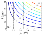
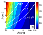
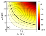
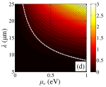
The extreme sensitivity of the PDP on the spatial period between the 2D planes makes the use of regular materials as dielectric hosts impractical, unless the dielectric host is also a 2D material with atomic scale control of the thickness and no roughness. For instance, one could build the dielectric host by stacking 2D layers of materials like hBN NanoTech10_2015 ; ACSNano6_2012 or molybdenum disulfide (MoS2) ACS12_2013 ; NatCom6_2015 ; Rodrick with essentially perfect planarity, complementing the planarity of graphene, which has been used extensively in optoelectronic and plasmonic applications NatPhot6_2012_review . The surface conductivity of an infinite graphene plane includes both intraband and interband transition contributions JModB27_2013 , with the intraband contribution dominating at THz frequencies which is approximated by the Drude model, , where is the tunable chemical potential and is the transport scattering time of the electrons NanoLet14_2014 ; PRL109_2012 ; NatPhot6_2012_review ; Photonics12_2014 . In the following, we use bulk MoS2, which at THz frequencies is assumed lossless with a diagonal permittivity tensor of elements, (out of plane) and (in plane) ACS12_2013 ; NatCom6_2015 ; Rodrick . The optical losses of graphene are taken into account using ps PRL109_2012 . In Fig. 2, we show the combinations of and the operational wavelength in free space which lead to a PDP for several values of lattice density distances in .
The ENZ behavior should be accompanied by low effective losses, otherwise the propagating field is damped fast. A crucial quantity demonstrating the efficiency of the proposed medium is the length that an EM wave can propagate into such a device without losing a significant part of its power. We find that the length before the amplitude falls to the of its maximal value, in units of the period , is given by:
| (6) |
From Eq. (6), the propagating beam travels along for more lattice periods, the less lossy the graphene sheets and the denser the lattice. The seeming contradiction of longer propagation in a denser lattice can be explained by the stronger SPP coupling for smaller periods PRL109_2012 . Using the Drude model for gives . This is shown in Fig. 2 by a contour plot as a function of free-space wavelength and cell physical size , and takes values in the range several hundreds. The loss-unaffected transmission length in terms of the number of wavelength cannot be determined explicitly by Eq. (6), because depends on . Nevertheless, an explicit expression of in terms of the number of wavelengths can be calculated, in the context of the Drude model. Eq. (6) can be re-written as indicating that is inversely proportional to and has no dependence on the doping level . The proposed design exhibits no significant losses of the propagating wave even in long structures consisting of several hundred periods. Interestingly, the best results (smallest losses) do not require large graphene doping.
To illustrate, for a reasonable distance between successive graphene planes of , the real (Fig. 2) and imaginary (Fig. 2) permittivity values that can be emulated by this specific graphene-MoS2 architecture determine the device characteristics at different frequencies () and graphene doping levels (). Positive values of are relatively moderate and occur for larger frequencies and lower doping levels of graphene; on the other hand, is relatively small in the ENZ region as indicated by a dashed line in both graphs. Such a fact renders our theoretical assumptions for lossless structures quite realistic; however, losses become larger as gets more negative. As these results show, the extreme sensitivity of the PDP on can be turned into an advantage for device fabrication: the proper combination of and can be selected to produce a device that operates at a given frequency (), as the practical limitations of layer stacking () or graphene doping () dictate.
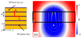
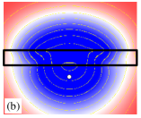
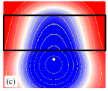
To examine the actual EM field distribution in our graphene-MoS2 configuration for each of the three characteristic cases of supported bands, we excite a finite structure consisting of 40 graphene planes and for operational wavelength in vacuum , using as a source a 2D magnetic dipole positioned close to one of its two interfaces and oriented parallel to them; this choice of source allows us to study the system’s response when exciting all the incidence angles with the same power. The spatial distribution of the magnetic field value is shown in Fig. 3 where the volume containing the graphene multilayers is denoted by a thick black frame. In all three cases, the reflections are negligible because the background region is filled with a medium of the same dielectric properties as MoS2. In Fig. 3, the system is in the critical case (), where the wave propagates through the graphene sheets without dispersion as in an ENZ medium. In Fig. 3, the interlayer distance is (strong SPP coupling regime) and the system shows negative (anomalous) diffraction with the front of the propagating wave into the multilayered structure showing a hyperbolic shape. In Fig. 3, (weak SPP coupling regime) and the EM wave shows ordinary diffraction through the graphene planes.
We acknowledge discussions with J. D. Joannopoulos, M. Soljacic, G.P. Tsironis, S. Shirodkar and P. Cazeaux, and support by EFRI 2-DARE NSF Grant 1542807 (MM), ARO MURI Award No. W911NF14-0247 (EK), the E.U. program FP7-REGPOT-2012-2013-1, grant 316165 (MM), and a SEED grant of Nazarbayev University for preliminary research (CAV). We used computational resources on the Odyssey cluster of the FAS Research Computing Group at Harvard University.
References
- (1) W. L. Barnes, A. Dereux, and T. W. Ebbesen, Nature 424, 825 (2003).
- (2) J. Dorfmüller, R. Vogelgesang, W. Khunsin, C. Rockstuhl, C. Etrich, K. Kern, Nano Lett. 10, 3596 (2010).
- (3) L. Huang et al., Nature Comm. 4, 2808 (2013).
- (4) J. Cheng, W. Li Wang, H. Mosallaei, and E. Kaxiras, Nano Lett. 14, 50 (2014).
- (5) D. Wintz, P. Genevet, A. Ambrosio, A. Woolf, and F. Capasso, Nano Lett. 15 3585 (2015).
- (6) H. Alaeian, and J. A. Dionne, Phys. Rev. A 89, 033829 (2014).
- (7) M. Mattheakis, T. Oikonomou, M. I. Molina, and G. P. Tsironis, IEEE Journal of Selected Topics in Quantum Electronics 22, 5 (2015).
- (8) C. A. Valagiannopoulos, IEEE Journal of Selected Topics in Quantum Electronics 22, 5 (2016).
- (9) T. Sfez et al., J. Opt. Soc. Am. B 27, 1617 (2010).
- (10) A. Block, C. Etrich, T. Limboeck, F. Bleckmann, E. Soergel, C. Rockstuhl, S. Linden, Nature Comm. 5, 3843 (2014).
- (11) B. Wang, X. Zhang, F. J. García-Vidal, X. Yuan, and J. Teng, Phys. Rev. Lett. 109, 073901 (2012).
- (12) Y. Liu, and X. Zhang, Appl. Phys. Lett. 103, 141101 (2013).
- (13) I. V. Iorsh, I. S. Mukhin, I. V. Shadrivov, P. A. Belov, and Y. S. Kivshar, Phys. Rev. B 87, 075416 (2013).
- (14) C. A. Valagiannopoulos, and S. A. Tretyakov, New J. of Phys. 16, 063004 (2014).
- (15) C. A. Valagiannopoulos, M. S. Mirmoosa, I. S. Nefedov, S. A. Tretyakov, and C. R. Simovski, J. Appl. Phys. 116, 163106 (2014).
- (16) A. A. High, R. C. Devlin, A. Dibos, M. Polking, D. S. Wild, J. Perczel, N. P. de Leon, M. D. Lukin, and H. Park, Nature 522, 192 (2015).
- (17) A. Alù, M. Silveirinha, A. Salandrino, and N. Engheta, Phys. Rev. B 75, 155410 (2007).
- (18) M. Silveirinha, and N. Engheta, Phys. Rev. Lett. 97, 157403 (2006).
- (19) M. A. K. Othman, C Guclu, and F. Capolino, J. of Nanophotonics 7, 073089 (2013).
- (20) Y. Liu, G. Bartal, D. A. Genov, and X. Zhang, Phys. Rev. Lett. 99, 153901 (2007).
- (21) Y. V. Bludov, D. A. Smirnova, Y. S. Kivshar, N. M. R. Peres, and M. I. Vasilevskiy, Phys. Rev. B 91, 045424 (2015).
- (22) M. S. Tame, K. R. McEnery, S. K. Özdemir, J. Lee, S. A. Maier, and M. S. Kim, Nature Physics 9, 329 (2013).
- (23) S. Dai et al., Nature NanoTech. 10, 682 (2015).
- (24) K. K. Kim, A. Hsu, X. Jia, S. M. Kim, Y. Shi, M. Dresselhaus, T. Palacios, and J. Kong, ACS Nano 6, 8583 (2012).
- (25) E. J. G. Santos, and E. Kaxiras, ACS Nano 7, 10741 (2013).
- (26) X. Chen et al., Nature Comm. 6, 6088 (2015).
- (27) R. K. Defo, S. Fang, S. N. Shirodkar, G. Tritsaris, A. Dimoulas, and E. Kaxiras, (2016) (submitted).
- (28) M. Jablan, H. Buljan, and M. Soljac̆ić, Phys. Rev. B 80, 245435 (2009).
- (29) A. N. Grigorenko, M. Polini, and K. S. Novoselov, Nature Photonics 6, 749 (2012).
- (30) R. L. Chern, and D. Han, Opt. Express 22, 4817 (2014).
- (31) B. Wang X. Zhang, K. P. Loh, and J. Teng, J. Appl. Phys. 115, 213102 (2014).
- (32) Z. Fei et. al., Nature 487, 82 (2012).
- (33) Y. V. Bludov, A. Ferreira, N. M. R. Peres, and M. I. Vasilevskiy, Int. J. Mod. Phys. B. 27, 1341001 (2013).
- (34) E. Forati, and G. W. Hanson, New J. of Phys. 15, 123027 (2013)
- (35) H. Deng, F. Ye, B. A. Malomed, X. Chen, and N. C. Panoiu, Phys. Rev. B 91, 201402(R) (2015).
- (36) A. A. Orlov, S. V. Zhukovsky, I. V. Iorsh, and P. A. Belov, Photonics and Nanostructures - Fundamentals and Applications 12, 213 (2014).
- (37) S. V. Zhukovsky, A. Andryieuski, J. E. Sipe, and A. V. Lavrinenko, Phys. Rev. B 90, 155429 (2014).