Deterministic strain-induced arrays of quantum emitters
in a two-dimensional semiconductor
Abstract
An outstanding challenge in quantum photonics is scalability, which requires positioning of single quantum emitters in a deterministic fashion. Site positioning progress has been made in established platforms including defects in diamondMeijer et al. (2005); McLellan et al. (2016) and self-assembled quantum dotsJöns et al. (2013); Yang et al. (2016), albeit often with compromised coherence and optical quality. The emergence of single quantum emitters in layered transition metal dichalcogenide semiconductorsSrivastava et al. (2015); He et al. (2015); Koperski et al. (2015); Chakraborty et al. (2015); Tonndorf et al. (2015); Kumar et al. (2015); Kern et al. (2016); Kumar et al. (2016); Palacios-Berraquero et al. (2016) offers new opportunities to construct a scalable quantum architecture. Here, using nanoscale strain engineering, we deterministically achieve a two-dimensional lattice of quantum emitters in an atomically thin semiconductor. We create point-like strain perturbations in mono- and bi-layer WSe which locally modify the band-gap, leading to efficient funnelling of excitonsFeng et al. (2012); Castellanos-Gomez et al. (2013); Li et al. (2015) towards isolated strain-tuned quantum emittersKumar et al. (2015); Kern et al. (2016) that exhibit high-purity single photon emission. These arrays of non-classical light emitters open new vistas for two-dimensional semiconductors in cavity quantum electrodynamicsVahala (2003) and integrated on-chip quantum photonicsLodahl et al. (2015).
Nanoscale strain engineering of the electronic band structure to create quantum confinement has long been pursued in bulk semiconductors. In particular, the exploitation of local elastic strain to laterally confine carriers has been achieved in epitaxially grown heterostructures such as quantum wellsKash et al. (1989); Obermüller et al. (1999); Schülein et al. (2009) or wiresGershoni et al. (1990). Unfortunately, robust strain-induced quantum confinement of carriers suitably isolated from detrimental surface states in bulk systems has not been realized due to the combination of: i) the limited elastic strain possible before plastic deformation and ii) small vertical strain propagation distances. Optically active two-dimensional (2D) semiconductors with a high elastic strain limitBertolazzi et al. (2011) offer renewed opportunities for nanoscale strain engineering of three-dimensional quantum confinement, which we pursue here.
To achieve point-like strain perturbations in atomically thin WSe, we use an all-dry transfer techniqueCastellanos-Gomez et al. (2014) to transfer mechanically exfoliated flakes onto a substrate with a square lattice ( pitch) of dielectric nanopillars. This technique takes advantage of Van der Waals’ forces to ensure the two-dimensional (2D) flake conforms to the contours of the patterned substrate and induces significant elastic strain at the locations of the nanopillarsReserbat-Plantey et al. (2014); Li et al. (2015). A WSe flake consisting of mono-layer (1L) and bi-layer (2L) regions is shown in Figs. 1a and 1b before and after transfer, respectively. In Fig. 1b the nanopillars are identified by the change in contrast: the dark points in the micrograph correspond to locations of the nanopillars. The transferred flake’s topography is characterized by atomic force microscopy (AFM), as shown in Fig. 1c-d. Scanning electron imaging of the same region (Supp. Info. Fig. S1) confirms the same physical features. Figure 1d compares the cross-section of a bare nanopillar (#0 in Fig. 1c) with an aspect ratio (height to width) of to that of a flake over a nanopillar (#7 in Fig. 1c). While the flake conforms quite closely to nanopillar #7 without significant wrinkling, at most lattice positions the flake stretches over the nanopillar analogously to a canvas over a tent-pole. In particular, randomly oriented pleats emerging from nanopillars are observed as well as ripples which in some cases extend towards neighbouring nanopillars. These features are typical of 2D flakes suspended over corrugated substrates and can be further engineeredReserbat-Plantey et al. (2014). Importantly, for the pitch array used here, the wrinkles do not mask the point-like strain perturbation created by the nanopillars.
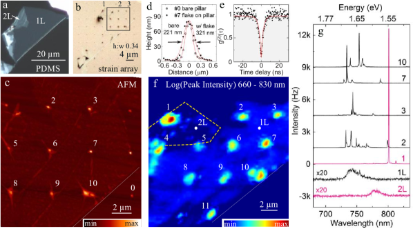
Hyperspectral confocal photoluminescence (PL) imaging is performed to fully characterize the atomically thin WSe flake and the effects of strain perturbations. Figure 1f shows a color-coded spatial map of the integrated intensity of the PL spectrum (). The PL intensity significantly increases at the locations of the nanopillars. The highly reduced PL signal in between the nanopillar sites is likely due to efficient diffusion of excitons towards the lower energy states at the strain-tuned sitesFeng et al. (2012); Castellanos-Gomez et al. (2013); Li et al. (2015). The spectra from several nanopillar sites as well as typical 1L and 2L regions between the nanopillars is exhibited in Fig. 1g. A broad defect band with weak intensity is observed in the homogeneous 1L and 2L regions (at low excitation powers the 2D excitons are not visible). On the other hand, for each spectrum obtained at a location of a nanopillar (including nanopillar #1 in the 2L region), a few discrete narrow linewidth () peaks with high intensity are typically observed. Each of these peaks signify emission from single quantum emittersSrivastava et al. (2015); He et al. (2015); Koperski et al. (2015); Chakraborty et al. (2015); Tonndorf et al. (2015); Kumar et al. (2015); Kern et al. (2016); Kumar et al. (2016); Palacios-Berraquero et al. (2016). A second-order correlation measurement is presented in Fig. 1e, where a fit to the data yields with a decay time of . This demonstrates photon antibunching and the quantum nature of the 1L discrete lines.
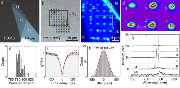
To demonstrate the universality of nanoscale strain engineering to generate strain-induced quantum emitters in atomically thin semiconductors, we create an array of pure single photon emitters in 2L WSe. Bi-layer WSe is an intriguing host for quantum emitters as it offers an additional pseudo-spin based on the layer degree of freedomJones et al. (2014). While 2L WSe is an intrinsically indirect band gap semiconductor, the indirect and direct transitions are nearly degenerate and under tensile strain the band structure can be modified such that the direct transition becomes preferredDesai et al. (2014). We exfoliate a flake with a large 2L region (see Fig. 2a) and transfer it to an array of nanopillars (with h:w ) on a Si substrate (Fig. 2b). Once again, we observe a huge increase in PL intensity at the nanopillar sites (Fig. 2c), evidencing the transition to a direct electronic gap and the exciton funnel effect due to local strain. We note there is also a small 1L and a large 3L region of the flake in Fig. 2b that cover nanopillar sites. While the 1L region shows similar properties to the flake in Fig. 1a, the 3L remains dark in PL. Crucially, bright narrow-linewidth spectral lines (Fig. 2h) are again observed at the strain-induced sites. Figure 2d shows a high-resolution spatial map of 6 nanopillars in the center of the array superimposed with the locations of the quantum emitters in Fig. 2h. A wavelength histogram ( binning) of all strain-induced emitters (53 in total) created in the 2L WSe array is shown in Fig. 2e. The histogram shows that emitters span a wavelength region from to . A Gaussian fit to the data is used to quantify the inhomogeneous distribution of the emitters, yielding full width at half maximum (FWHM). Notably, several emitters at very similar wavelengths are observed (e.g. in Fig. 2h peaks at in spectra 2 and 5; peaks at in spectra 1 and 3). The second order correlations from each individual peak measured exhibit highly pure single photon emission, e.g the single peak at from nanopillar #1 in Fig. 1g shows with a decay time of (Fig. 2f). For spectra recorded over a 20 hour period, this emitter does not blink. Figure 2g shows a histogram of the spectral jitter recorded over 20 hours (using 3 s time-bin) from the 2L emitter at nanopillar #1. The histogram is fit by a Gaussian distribution with FWHM. Further, these quantum emitter arrays are optically stable and robust, surviving multiple sample cooling and heating cycles.
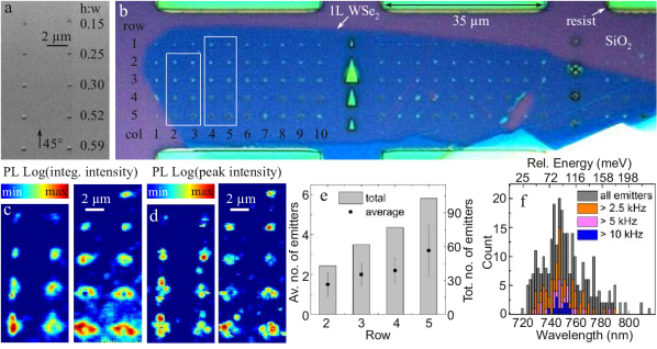
Having established a technique to successfully create robust strain-induced quantum emitters, we seek to optimize the process. We tailor the local elastic strain by varying the height to change the aspect ratio of five rows of nanopillars, from h:w 0.15 to 0.59, as shown in the scanning electron micrograph in Fig. 3a. Precise measurements of the pillar size are made by AFM (see Supp. Info. Fig. S3). Figure 3b shows an optical micrograph of a large () 1L WSe flake covering 101 nanopillars in the array. Here the pillar locations are identified by the bright points in the micrograph. Also visible in Fig. 3b in some cases for the high aspect ratio nanopillars (e.g. Row 5, Columns 3–5) is a small ring surrounding the pillar. We show in the following that in such cases the pillar has punctured the 2D flake during the transfer process. Flake puncturing is not observed for any of the low aspect ratio nanopillars in Rows 1 and 2 or with the nanopillars used in Figs. 1 and 2. Figure 3c shows a spatial map of the integrated intensity (logarithmic scale) of the entire PL spectrum () from Columns 2 – 5 (as labelled in Fig. 3b). PL maps of the entire flake with several spectra are shown in the Supplementary Information (Fig. S4). A mixture of peaks with large () fine-structure splittings (e.g. Fig. S5) and single linearly polarised peaks are observed, as reported previouslyKumar et al. (2016). The PL intensity at the nanopillars increases with increasing nanopillar aspect ratio, as expected for the diffusion of excitons towards the local regions with strain-tuned band-gaps. Further, in the cases where the flake is pierced, low intensity PL at the nanopillar center is surrounded by a ring of intense PL.
Figure 3d maps the locations of the intense, narrow linewidth peaks that signify quantum light emission in Columns 2 – 5. We determine the positioning accuracy of the strain-induced quantum emitters by comparing their location to the center of the nanopillars (see Fig. S6 for the measurement of the nanopillar centre). We observe that when the flake is pierced by a nanopillar, the emitters are found at the circumference of the nanopillar. On the other hand, the quantum emitters are created in the center of the nanopillars for flakes that conform to the substrate topography. In particular, the positioning accuracy of the emitters in Row 2 reveal high precision for positioning accuracy: , where is the average displacement of the emitter from the nanopillar center. Displacement statistics of the emitters in Rows 3 – 5 are: , , and . Row 1 did not yield sufficient emitter numbers for useful statistics. In the best case (Column 5, Row 2), the displacement is . While this accuracy is sufficient to couple to cavity or waveguide modes for cavity quantum electrodynamics experiments and integrated quantum photonics applicationsVahala (2003); Lodahl et al. (2015), further improvements for more precise and robust positioning of single emitters is likely possible with smaller diameter nanopillars that maintain an aspect ratio similar to Row 2.
Statistics of all emitters identified (285 in total) in the entire 1L WSe flake over the 101 nanopillars is shown in Fig. 3e and f. Figure 3e shows the statistics for the number of emitters per pillar. While distinct emitters are sometimes found at the nanopillar sites in Row 1 (e.g. the spectra in Fig. S4c), they tend to be difficult to distinguish from the broad background. With the increased aspect ratio of the nanopillars in Row 2, one or two distinct bright emitters are found with a yield of 85% (17 of 20 nanopillars contain pure single emitters). Rows 3 and 4 have near unity yields: 96% (45 of 47 nanopillars yield at least 1 quantum emitter). Figure 3f shows the emitter wavelength histogram. While the overall energy distribution of the single emitters is broad (spanning ), all emitters emit at lower energy than the bright 2D exciton peak in WSe (Wang et al. (2014)). The emitter wavelength histogram is also post-selected for emitter brightness (the peak intensity at saturation power) for this flake. Fitting a Gaussian distribution to the histogram gives FWHM, more than twice as large as the 2L emitters.
Layered transition metal dichalcogenide semiconductors are attractive hosts for quantum emitters due to the unique valley degree of freedom and strong spin-orbit coupling. Using nanoscale elastic strain engineering, we have achieved local modification of the electronic and optical properties to deterministically generate robust quantum emitters in this emerging quantum photonic platform. The straightforward fabrication procedure presented here is scalable and likely to be applicable to other 2D materials. Notably, we observe negligible background signal at the base of the discrete spectral lines, enabling high purity single photon emission in both 1L and 2L WSe. Compared to mono-layer WSe, the bi-layer appears additionally attractive as a host for single excitons due to a narrower inhomogenous distribution and the potential for spin-layer locking.
We thank N. Ross for assistance with electron beam lithography. This work was supported by a Royal Society University Research Fellowship, the EPSRC (grant numbers EP/I023186/1, EP/K015338/1, EP/L015110/1, and EP/M013472/1) and an ERC Starting Grant (number 307392).
References
- Meijer et al. (2005) J. Meijer, B. Burchard, M. Domhan, C. Wittmann, T. Gaebel, I. Popa, F. Jelezko, and J. Wrachtrup, Appl. Phys. Lett. 87, 261909 (2005).
- McLellan et al. (2016) C. A. McLellan, B. A. Myers, S. Kraemer, K. Ohno, D. D. Awschalom, and A. C. Bleszynski Jayich, Nano Lett. 16, 2450 (2016).
- Jöns et al. (2013) K. D. Jöns, P. Atkinson, M. Müller, M. Heldmaier, S. M. Ulrich, O. G. Schmidt, and P. Michler, Nano Lett. 13, 126 (2013).
- Yang et al. (2016) L. Yang, S. G. Carter, A. S. Bracker, M. K. Yakes, M. Kim, C. S. Kim, P. M. Vora, and D. Gammon, Appl. Phys. Lett. 108, 233102 (2016).
- Srivastava et al. (2015) A. Srivastava, M. Sidler, A. V. Allain, D. S. Lembke, A. Kis, and A. Imamoglu, Nat. Nanotechnol. 10, 491 (2015).
- He et al. (2015) Y.-M. He, G. Clark, J. R. Schaibley, Y. He, M.-C. Chen, Y.-J. Wei, X. Ding, Q. Zhang, W. Yao, C.-Y. Xu, Xiaodongand Lu, and J.-W. Pan, Nat. Nanotechnol. 10, 497 (2015).
- Koperski et al. (2015) M. Koperski, K. Nogajewski, A. Arora, J. Marcus, P. Kossacki, and M. Potemski, Nat. Nanotechnol. 10, 503 (2015).
- Chakraborty et al. (2015) C. Chakraborty, L. Kinnischtzke, K. M. Goodfellow, R. Beams, and A. N. Vamivakas, Nat. Nanotechnol. 10, 507 (2015).
- Tonndorf et al. (2015) P. Tonndorf, R. Schmidt, R. Schneider, J. Kern, M. Buscema, G. A. Steele, A. Castellanos-Gomez, H. S. van der Zant, S. Michaelis de Vasconcellos, and R. Bratschitsch, Optica 2, 347 (2015).
- Kumar et al. (2015) S. Kumar, A. Kaczmarczyk, and B. D. Gerardot, Nano Lett. 15, 7567 (2015).
- Kern et al. (2016) J. Kern, I. Niehues, P. Tonndorf, R. Schmidt, D. Wigger, R. Schneider, T. Stiehm, S. Michaelis de Vasconcellos, D. E. Reiter, T. Kuhn, and R. Bratschitsch, Adv. Mater. 28, 7101 (2016).
- Kumar et al. (2016) S. Kumar, M. Brotóns-Gisbert, R. Al-Khuzheyri, A. Branny, G. Ballesteros-Garcia, J. F. Sánchez-Royo, and B. D. Gerardot, Optica 3, 882 (2016).
- Palacios-Berraquero et al. (2016) C. Palacios-Berraquero, M. Barbone, D. M. Kara, X. Chen, I. Goykhman, D. Yoon, A. K. Ott, J. Beitner, K. Watanabe, T. Taniguchi, A. C. Ferrari, and M. Atatüre, Nat. Commun. 7, 12978 (2016).
- Feng et al. (2012) J. Feng, X. Qian, C.-W. Huang, and J. Li, Nature Photonics 6, 866 (2012).
- Castellanos-Gomez et al. (2013) A. Castellanos-Gomez, R. Roldán, E. Cappelluti, M. Buscema, F. Guinea, H. S. van der Zant, and G. A. Steele, Nano Lett. 13, 5361 (2013).
- Li et al. (2015) H. Li, A. W. Contryman, X. Qian, S. M. Ardakani, Y. Gong, X. Wang, J. M. Weisse, C. H. Lee, J. Zhao, P. M. Ajayan, J. Li, H. C. Manoharan, and X. Zheng, Nat. Commun. 6, 7381 (2015).
- Vahala (2003) K. J. Vahala, Nature 424, 839 (2003).
- Lodahl et al. (2015) P. Lodahl, S. Mahmoodian, and S. Stobbe, Rev. Mod. Phys. 87, 347 (2015).
- Kash et al. (1989) K. Kash, R. Bhat, D. D. Mahoney, P. S. D. Lin, A. Scherer, J. M. Worlock, B. P. Van der Gaag, M. Koza, and P. Grabbe, Appl. Phys. Lett. 55, 681 (1989).
- Obermüller et al. (1999) C. Obermüller, A. Deisenrieder, G. Abstreiter, K. Karrai, S. Grosse, S. Manus, J. Feldmann, H. Lipsanen, M. Sopanen, and J. Ahopelto, Appl. Phys. Lett. 74, 3200 (1999).
- Schülein et al. (2009) F. J. R. Schülein, A. Laucht, J. Riikonen, M. Mattila, M. Sopanen, H. Lipsanen, J. J. Finley, A. Wixforth, and H. J. Krenner, Appl. Phys. Lett. 95, 083122 (2009).
- Gershoni et al. (1990) D. Gershoni, J. S. Weiner, S. N. G. Chu, G. A. Baraff, J. M. Vandenberg, L. N. Pfeiffer, K. West, R. A. Logan, and T. Tanbun-Ek, Phys. Rev. Lett. 65, 1631 (1990).
- Bertolazzi et al. (2011) S. Bertolazzi, J. Brivio, and A. Kis, ACS Nano 5, 9703 (2011).
- Castellanos-Gomez et al. (2014) A. Castellanos-Gomez, M. Buscema, R. Molenaar, V. Singh, L. Janssen, H. S. J. van der Zant, and G. A. Steele, 2D Materials 1, 011002 (2014).
- Reserbat-Plantey et al. (2014) A. Reserbat-Plantey, D. Kalita, Z. Han, L. Ferlazzo, S. Autier-Laurent, K. Komatsu, C. Li, R. Weil, A. Ralko, L. Marty, S. Guéron, N. Bendiab, H. Bouchiat, and V. Bouchiat, Nano Lett. 14, 5044 (2014).
- Jones et al. (2014) A. M. Jones, H. Yu, J. S. Ross, P. Klement, N. J. Ghimire, J. Yan, D. G. Mandrus, W. Yao, and X. Xu, Nat. Phys. 10, 130 (2014).
- Desai et al. (2014) S. B. Desai, G. Seol, J. S. Kang, H. Fang, C. Battaglia, R. Kapadia, J. W. Ager, J. Guo, and A. Javey, Nano Lett. 14, 4592 (2014).
- Wang et al. (2014) G. Wang, L. Bouet, D. Lagarde, M. Vidal, A. Balocchi, T. Amand, X. Marie, and B. Urbaszek, Phys. Rev. B 90, 075413 (2014).
Supplementary material: Deterministic strain-induced arrays of quantum emitters
in a two-dimensional semiconductor
This supplementary information gives insight into detailed aspects of the results. These additional measurements allow for better understanding of the samples and quantum emitters behaviour in monolayer and bilayer WSe.
Figure S1 shows scanning electron microscope (SEM) images of a monolayer WSe transferred onto the nanopillars. The topography observed here matches that observed in the atomic force microscope (AFM) image of Fig. 1c in the main article. A magnification of the areas framed in Fig. S1a is presented in Fig. S1b, c and d. The wrinkled monolayer around nanopillar 6 is clearly visible in Fig. S1c. Figure S1d shows a bare nanopillar for comparison (identified by a white square at the bottom right of Fig. S1).
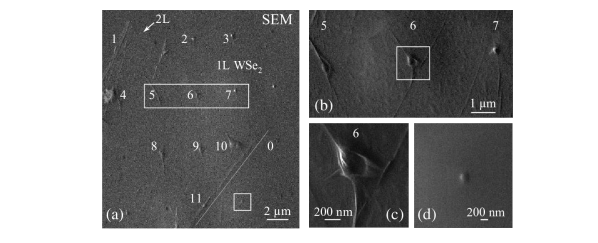
Figure S2 characterizes more precisely the 2L emitter 1 of Fig. 1 of the main article. Figure S2a shows a time-trace of the peak energy over 20 hours of measurement. The standard deviation is ), showing good emission energy stability. Figure S2b is an intensity histogram performed on the same time-trace measurement. It accounts for an excellent intensity stability with no blinking observed. The majority of intensity fluctuations are due to vibrations during the period. Finally, Figure S2 is a power dependence of the integrated photoluminescence intensity. The emitter exhibits a very clear saturation behaviour consistent with a two-level system.

Figure S3 shows the nanopillars characterization on the same sample as Fig. S4, prior to the deposition of the monolayer WSe. Figure S3a are vertical profiles of the nanopillars for each row. Figure S3b displays the dimensions and aspect ratio extracted from Fig. S3a. The width stays constant at for all rows while the height increases from to . Figure S3c is an SEM image of the sample, where the different rows of nanopillars are visible corresponding to different aspect ratios. Figure S3d is a magnification of nanopillars from rows 2, 3 and 4. The change in height is clearly visible.
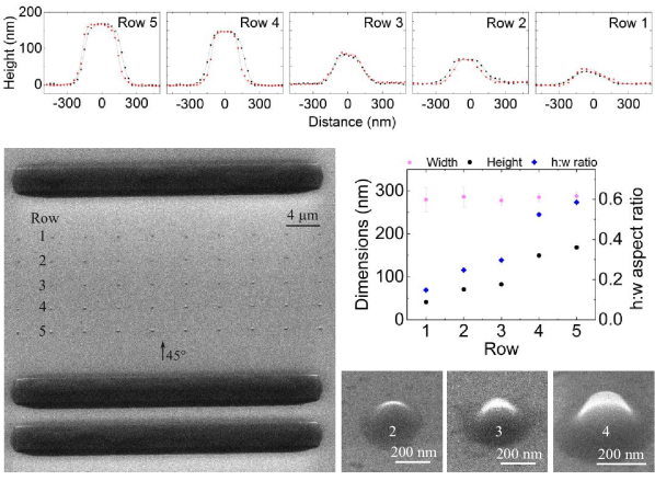
Figure S4 shows more extensive data on the monolayer WSe sample displayed in Fig. 3 of the main article. Figure S4a shows the larger view of the same optical micrograph as Fig. 3b. Figure S4b shows 4 different spatial maps stitched together displaying the integrated photoluminescence intensity on the color scale. PL intensity is systematically enhanced at the position of the nanopillars. Figure S4c shows several photoluminescence spectra for diverse quantum emitters on the position of the nanopillars.
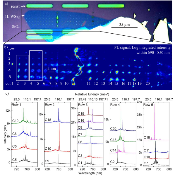
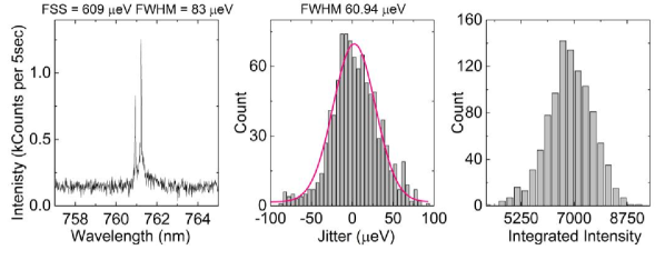
Figure S5 shows the results from a time-trace measurement from the emitter at nanopillar #2 in the 1L flake from Fig. 1 in the main text. The left panel is a PL emission spectrum presenting a fine structure-splitting of . This spectrum is part of a time-trace measurement of with time bins. The center graph is an energy histogram integrated from the time-trace. The PL peak energy fluctuates . Finally, the right panel is an intensity histogram showing the non-blinking behaviour, with a mean intensity of counts per time bin.
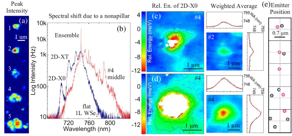
The position of the nanopillars in the hyperspectral spatial maps is not known a priori. We therefore use a spectral weighted averaging (WA) method to determine the centre position of the nanopillars.
Figure S6 illustrates this process. First, Fig. S6a shows a high definition spatial map of the spectral peak intensity. The individual emitters are resolved but the accurate position of the centre of the nanopillars is unknown. Figure S6b shows two PL spectra: one off the nanopillar and one on a nanopillar. Strain induces a global shift in the energy of the spectrum. We assume that the strain experienced by the flake is at its highest in the middle of the nanopillar. Thus, taking the mean emission energy and mapping its shift with position enables us to determine the position of the nanopillars with high accuracy. Figures S6c and d show spatial maps for the energy of the 2D exciton (2D-X0) on the left and average wavelength weighted by the intensity on the right. The weighted average is computed using:
| (1) |
where is the intensity.
The energy of the 2D exciton also shifts with strain, and has been previously used to estimate the strainKumar et al. (2015). However, only the can fully map the nanopillar in the data presented here. The white region in the middle of 2D-X0 is where the 2D-X0 intensity vanishes at higher strains. On the other hand, the profile of weighted average yields a smooth, clean contour map from which the centre of nanopillars can be accurately determined.
Figure S6e shows the assessed positions of the emitters (circle markers) compared to the position of the centre of the nanopillars in Column 5 (grey crosses) determined using the weighted average method.
