Characterization of single layer anti-reflective coatings for bolometer-based rare event searches
Abstract
Combining analysis from phonon signals and photon signals is a powerful technique for reducing backgrounds in bolometer-based rare event searches. Anti-reflective coatings can significantly increase the performance of the secondary light-sensing bolometer in these experiments. As a first step toward these improvements, coatings of SiO2, HfO2, and TiO2 on Ge and Si wafers were fabricated and characterized at room temperature and multiple angles of incidence.
keywords:
radiation detector, scintillating bolometers, double beta decay, antireflective coatings1 Introduction
Rare-event searches are being pursued to answer some of the greatest mysteries in physics at the present time, namely: the nature of dark matter through direct detection (DM) and the possible Majorana nature of the neutrino through searches for neutrinoless double-beta decay (). In these experiments, combining multiple signals is a powerful active background rejection technique. Scintillating bolometers use the combination of phonon and photon signals to discriminate between particle types. The CUPID (CUORE with Upgraded Particle IDentification) [1] and CRESST [2, 3] detectors are pursuing this technology for and DM searches respectively.
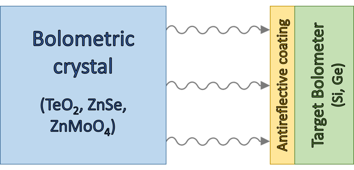
A scintillating bolometer measures a phonon signal: the change in temperature in a crystal due to the interaction of charged particles with the crystal lattice. These interactions also produce a photon signal: scintillation light which is detected by a target Ge or Si bolometer. An anti-reflective coating on the target bolometer, as shown in Figure 1, increases light collection and therefore improves the energy resolution of the light measurement. In this paper, we discuss the optimization of an anti-reflective coating for two promising scintillating crystals containing isotope: ZnSe and ZnMoO4. We also discuss optimizing the anti-reflective coating to detect Cherenkov light in non-scintillating crystals like TeO2, the current CUORE crystal.
2 Light Emission and Simulation
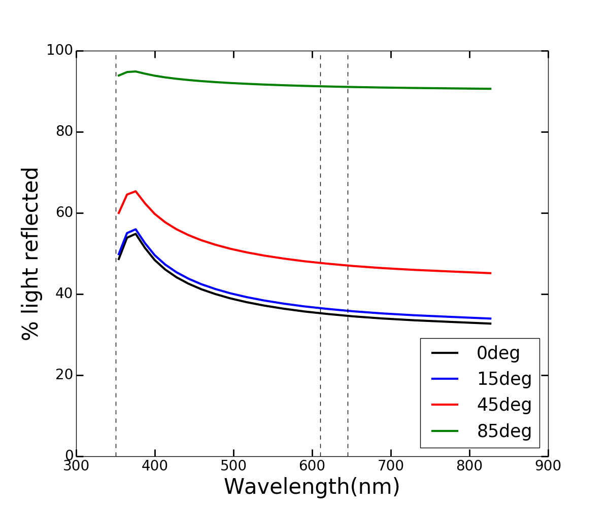
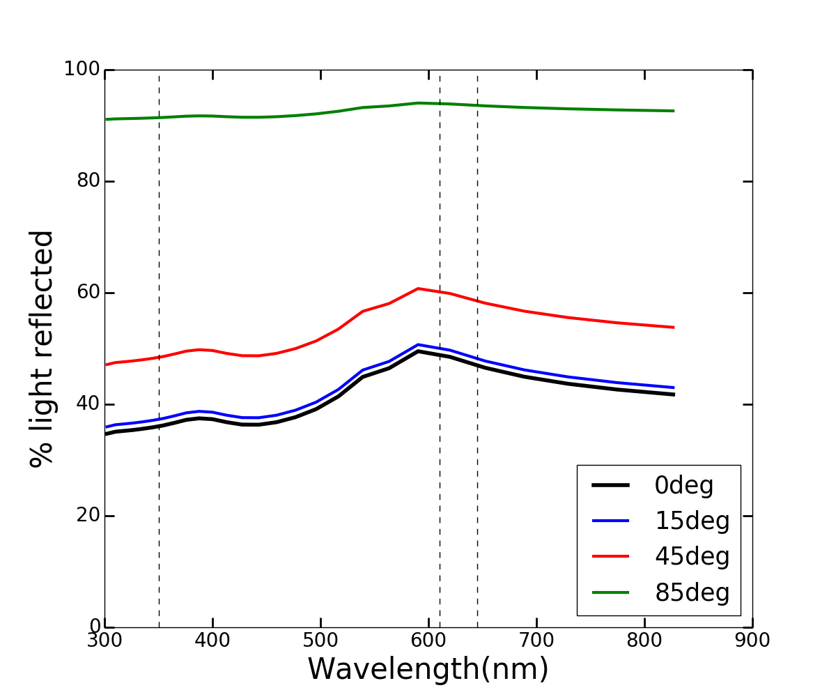
The scintillation spectra of ZnSe and ZnMoO4 are well characterized at temperatures down to 8 K. The spectra peak at 645 nm and 610 nm respectively [4]. The absorption cutoff for TeO2 is 350 nm [5], forming the effective peak of the Cherenkov spectrum. Our default target bolometer is composed of hyper-pure germanium (HPGe) thin slabs run at a standard operating temperature of 15-20 mK. We also study silicon (Si) since it has equivalent performance at these operating temperatures and is widely available. Using refractive index data from [6], we find Ge substrates reflect 50% of normal incident light while Si substrates reflect 35%; see Figure 2. The results for ZnSe scintillation at 645 nm and TeO2 Cherenkov light are similar.
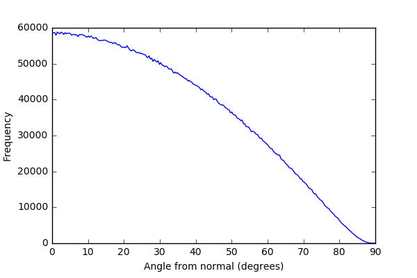
As shown in Figure 2, the angle of incidence is critical for understanding the response of the target bolometer. A GEANT4[7, 8, 9] Monte Carlo was constructed to examine the incidence angles of photons produced from beta particles distributed isotropically in position, angle, and energy throughout a ZnMoO4 bolometer. The light produced from these events was allowed to scatter within the crystal until it attenuated, escaped, or struck a target bolometer 1mm away from a single face. The relevant physical and optical properties of these materials, if not specifically included in the Geant4 NIST database, were obtained from literature[10, 11, 12]. Results are shown in Figure 3. The average angle of incidence was 32∘ with a standard deviation of 21∘. This is a sizable deviation from normal incidence, and must be considered when selecting a coating/bolometer combination. In future work, the results of these measurements for the final target bolometers can be used either as input to or a benchmark of the Monte Carlo.
3 Anti-Reflective Coatings
As seen in Figure 1, the target bolometer can be supplemented by depositing an anti-reflective coating to create a thin film structure where layers of contrasting refractive indices produce destructive interference in reflected beams and constructive interference in transmitted beams. This results in an overall increase of transmission. The performance of this structure depends heavily on the light’s incident angle, wavelength, and polarization. The reflection coefficient for unpolarized light incident on a single layer anti-reflective coating (SLAR) is written [13] as:
| (1) |
| (2) |
where the subscripts and refer to waves parallel or perpendicular to the plane of incidence and the numerical subscripts refer to the medium in which the light is traveling: 0 for the outside medium (ideally vacuum), 1 for the SLAR, and 2 for the substrate. If is the angle of incidence onto the SLAR of thickness , the phase shift is given by . The individual reflection coefficients are given by
| (3) |
and
| (4) |
where and are the real and imaginary parts, respectively, of the complex refractive index of the material and are also dependent on wavelength. The ideal coating will minimize with respect to and .
| Material | () | |
|---|---|---|
| ZnSe | 2.58 (645 nm) [14] | 22.8∘ |
| ZnMoO4 | 1.90 (655 nm)⋆ [15] | 31.7∘ |
| TeO2 | 2.25 (645 nm) [16] | 26.4∘ |
3.1 Comparison to Previous Experiment (Mancuso, Beeman, et.al.)
This work builds upon the study done by Mancuso et al. [17]. They tested SiO2 films, 70 nm thick and deposited on a Ge substrate using a sputtering technique. The films were evaluated at 10 mK. SiO2 decreased reflectivity by 18-20% [17]. In this paper, we manufacture similar coatings but characterize them at room temperature so that we can study the angular effects.
In Mancuso et.al., the scintillation light is assumed to reach the target bolometer at normal incidence. As we show in Section 2 and as they indicate in their paper, this is a crude assumption. From first principles, the refractive index in the crystals of interest, ZnSe, ZnMoO4, and TeO2, is high enough to allow total internal reflection at a relatively low angle; see Table 1. This implies that even a slight deviation from normal (in the plane of incidence) as the ray leaves the primary bolometer can cause the refracted ray to deviate significantly from normal as it strikes the target bolometer. The distance between primary and target bolometers is small enough (1 cm) that the angle of incidence on the target bolometer will range from 0∘ to roughly 88∘ in the plane of incidence (assuming a CUORE-sized 5cm5cm crystal). From Equations 1-4, it is clear that a phase difference between reflected waves from the film layer and reflected waves from the substrate layer is introduced whenever the incident angle is non-normal, leading to a substantial change in reflectivity for non-normal incidence.
3.2 Choice of Substrates
Ge is the logical choice for the target bolometer because it absorbs photons better than Si in the visible range; the absorption coefficient of Ge is roughly two orders of magnitude greater [18]. However, Si is more readily available and the manufacturing processes are extremely well understood. These include techniques that could improve anti-reflective coatings, such as micromachining and deposition masking [19]. Finally, Ge has a specific heat 4.5 times greater than that of Si [20]. Because signal amplitude is inversely proportional to the heat capacity of the device, Si detectors can be made into much larger systems without sacrificing signal quality [21]. Considering these factors, we chose to study both Ge and Si as target bolometer candidates for this work.
3.3 Choice of Coatings
For a particular substrate, the minimum possible reflectivity using a SLAR can be calculated using the curves from Equation 1. For a Ge substrate and incident 645 nm light from the ZnSe scintillation peak, the complex refractive index of Ge has components and . Assuming no losses to the thin film and normal incidence, the reflection coefficient can be decreased maximally with a coating medium with refractive index . The closest match considering available materials is TiO2; see Table 2. HfO2 is also a possibility. Performing the same calculation for a Si substrate, the minimum reflectivity is achieved for a coating with . Si3N4, HfO2, and Al2O3 (sapphire) are good matches.
| Material | n (645nm) | Source |
|---|---|---|
| Al2O3 | 1.76 | Malitson (1972) [22] |
| HfO2 | 2.10 | Wood (1990) [23] |
| Si3N4 | 2.00 | Philipp (1973) [24] |
| SiO2 | 1.48 | Gao (2013) [25] |
| TiO2 | 2.58 | Devore (1951) [26] |
A second anti-reflective layer can be used to further reduce reflectivity. The optimization proceeds similarly to above, except that, in this case, the refractive index is tuned to the first coating instead of the substrate. For example, a Ge-TiO2 target system could be improved by adding second coating with a refractive index of . GeO2 ( [27]) is not readily available, but the more common SiO2 is a good candidate. Traditionally, SiO2 has been used as a single layer coating for Si substrates because it is readily available, easily manufactured, and has better mechanical strength and adhesion under thermal cycling. In this work, we focus on single layer coatings, but future work will include two layer systems.
As previously noted, the performance of the anti-reflective coating is dependent on the angle of the incoming light. Using equation 1 for non-normal incidence, reflection curves were plotted for use in selecting SLAR candidates; these curves for SiO2 on Si and Ge substrates can be seen in Figure 4. The coating always improves the performance of the target bolometer. However, the improvement may not be sufficient to overcome the increased complexity and cost of adding the coating.
The above calculations assume all reflections are specular, the refractive index is constant throughout the thickness of the SLAR, and there are no losses in the SLAR (). The incident light is also assumed to be unpolarized. This final assumption is not valid for TeO2 due to birefringence. In this case, the refractive index varies between 1 and the true refractive index depending on the axis of propagation.
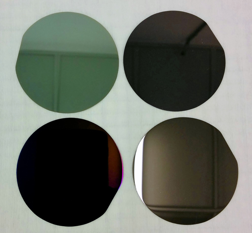
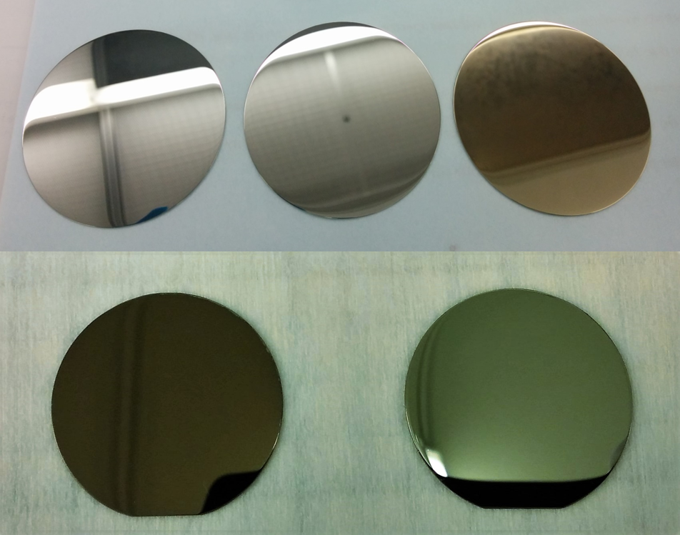
Based on their refractive index and availability, the following coatings were selected. For Ge, we study Al2O3, SiO2, TiO2, and HfO2. For Si, we study SiO2 and HfO2. Figure 5 shows the wafers produced for this study. Al2O3 is a promising candidate. We were not able to obtain the materials to deposit it on Si, so it was only used for Ge.
| Ge (1) | Ge (2) | Si | |
|---|---|---|---|
| Orientation | crystalline, <100> | crystalline <100> | crystalline, <100> |
| Thickness | 500 m | 350 m | 280 m |
| Diameter | 2 in | 1 in | 2 in |
| Doping | undoped | undoped | N Type, P Doped |
| Polish | 2SP | 1SP | 1SP |
| Resistivity | >50 cm | 30 cm | 1-100 cm (test) |
4 Other Requirements
In addition to the target bolometer’s optical properties, DM and requirements have stringent requirements on surface and bulk radioactivity contamination for detector components. A complete background model like that constructed for CUORE[28] will set these specifications for the coating and substrate. The CUPID program already has extensive experience with the procurement and handling of Ge and Si wafers. When the final candidate coating are chosen, the bulk material will need to be counted to ensure that it meets the desired specifications. Devoted tests will also be needed for understanding the coatings robustness under thermal cycling. This is all part of future work.
5 Fabrication
The 1-inch Ge wafers and 2-inch Si wafers were procured from University Wafer [29]. The 2 in Ge wafers were purchased from MTI Corporation [30]. Table 3 summarizes the properties of these wafers. The wafers were coated at the UCLA Nanoelectronics Research Facility (NRF) in a class-1000 multiuse cleanroom.
Al2O3, HfO2, TiO2 coatings
Non-silicate coatings were deposited using a Fiji thermal atomic layer deposition (ALD) system. In such a system, precursors were pulsed into an Argon atmosphere such that for each pulse a single atomic layer adhered to the surface of the wafer. Each wafer was loaded into the machine at room temperature and atmosphere, and processed at 200 ∘C and 0.02 mTorr.
Al2O3 was used as a test wafer. It is a common coating that starts from TMA (trimethylaluminum) or Al(CH3)3. For HfO2 coatings, precursors of Hf(NMe2)4 and H2O were pulsed at 0.06 sec each until the desired thickness was reached. For TiO2, coatings were processed similarly from a precursor of Tetrakis(Dimethylamido)Titanium (Ti(NMe2)4).
The ALD process was lengthy and required up to six hours to produce a single wafer. This technique has the advantage that more complex coating geometries can be achieved through nanopatterning. These geometries will be explored in future work.
SiO2 coatings
Silicate coatings were deposited using a High Deposition BMR plasma-enhanced chemical vapor deposition (PECVD). The system uses time-varying magnetic fields to generate highly dissociated plasmas of the precursor material which allows for a higher rate of deposition. Precursors of SiH4 and O2 gasses were used to create SiO2 films at rates of up to 3000 Å/min. In the case of the BMR PECVD, the input is a desired time of deposition (as opposed to a desired thickness). This led to less precision in the final thickness of the coating; however, this process was very efficient and several wafers of different thicknesses could be produced over the course of a few hours.
6 Characterization
Samples were characterized using fixed and variable angle ellipsometry. The coated substrates were subjected to unpolarized light at an angle which reflected into a detector to measure the relative amplitude and phase of s- and p-polarizations. Relative amplitudes and phases of polarizations are described as a function of wavelength and angle by two variables [13]:
| (5) |
which can be combined to measure the total ratio of polarized reflections.
| (6) |
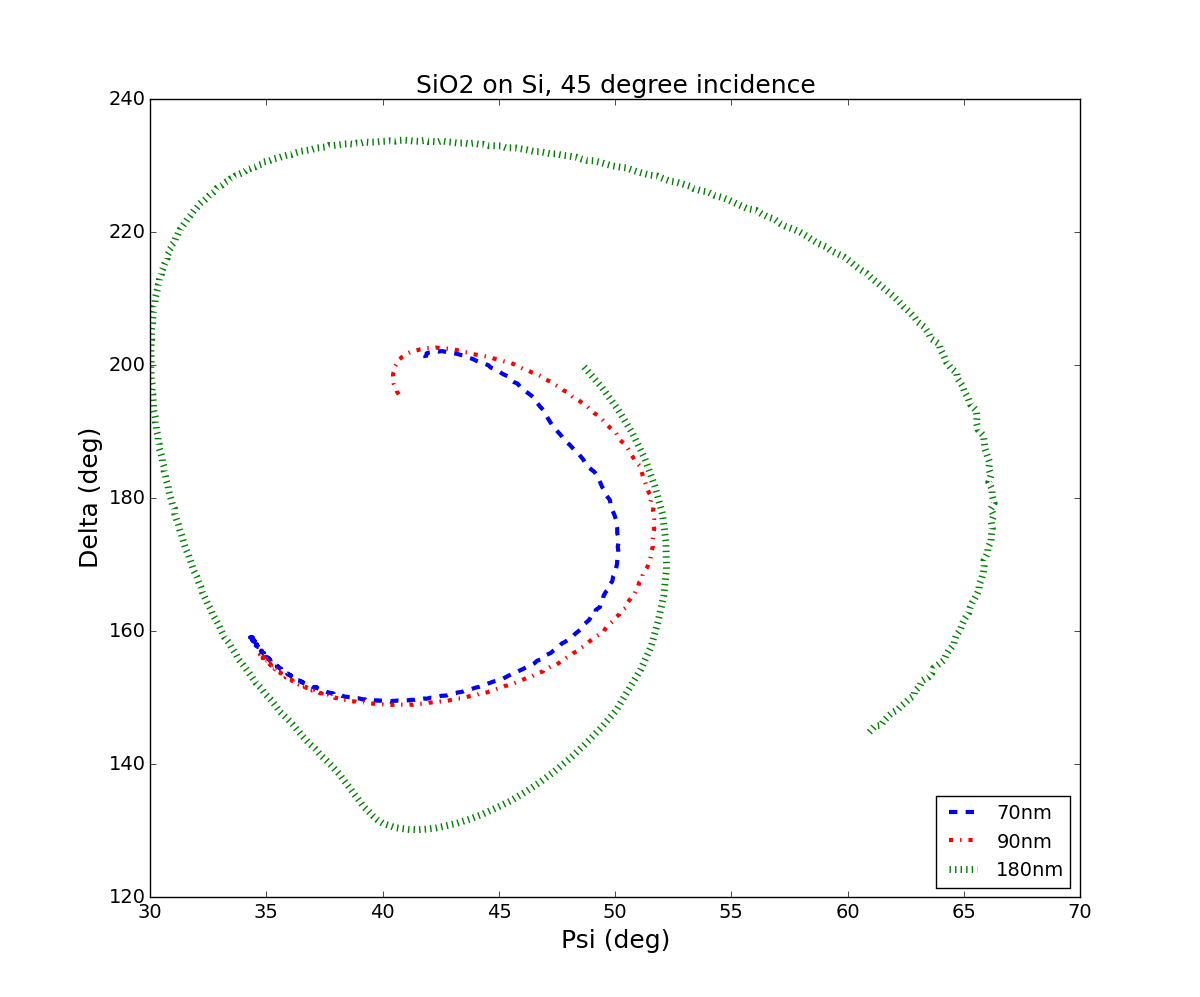
Figure 6 shows an example of representative data.
| Sample # | Substrate | Coating | Thickness (nm) (ULVAC) | Thickness (nm) (Woolam) |
|---|---|---|---|---|
| 1 | Si | SiO2 | 66.116 1.899 | 75.655 0.021 |
| 2 | Si | SiO2 | 79.627 1.245 | 90.09 0.49 |
| 3 | Si | SiO2 | 181.902 0.782 | 180.029 0.037 |
| 4 | Ge | SiO2 | – | 75.26 2.294 |
| 5 | Ge | SiO2 | – | 140.84 3.13 |
At this point, refractive index and thickness information for the coating was modeled and fit to experimental curves using equations 2-4. It was not possible to directly calculate total reflection from these measurements, but a satisfactory result was found by reusing the calculated refractive index and thickness in equations 1-4. It should be noted that the measurement error of and are systematic; calculations of film thickness and optical characteristics are model dependent.
The UCLA Nanoelectronics Research Facility ULVAC UNECS-2000 fixed angle ellipsometer was used for immediate characterization of the Si wafers. Ge is less common, so no model was available. The UCSB Nanofabrication Facility’s Woollam M2000DI VASE Spectroscopic Ellipsometer was used to fully characterize all samples at variable angles.
Film thickness and single-point were analyzed in two groups. The ULVAC companion software was used for normal incidence, and the Woollam ellipsometer’s companion software CompleteEase was used for variable angle incidence. The results are shown in Table 4. SiO2 coatings were assumed to follow Cauchy’s equation:
| (7) |
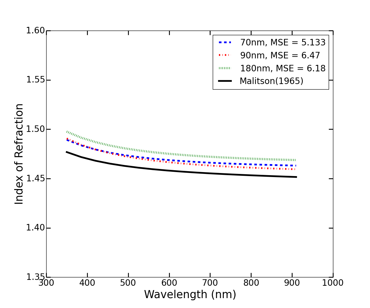
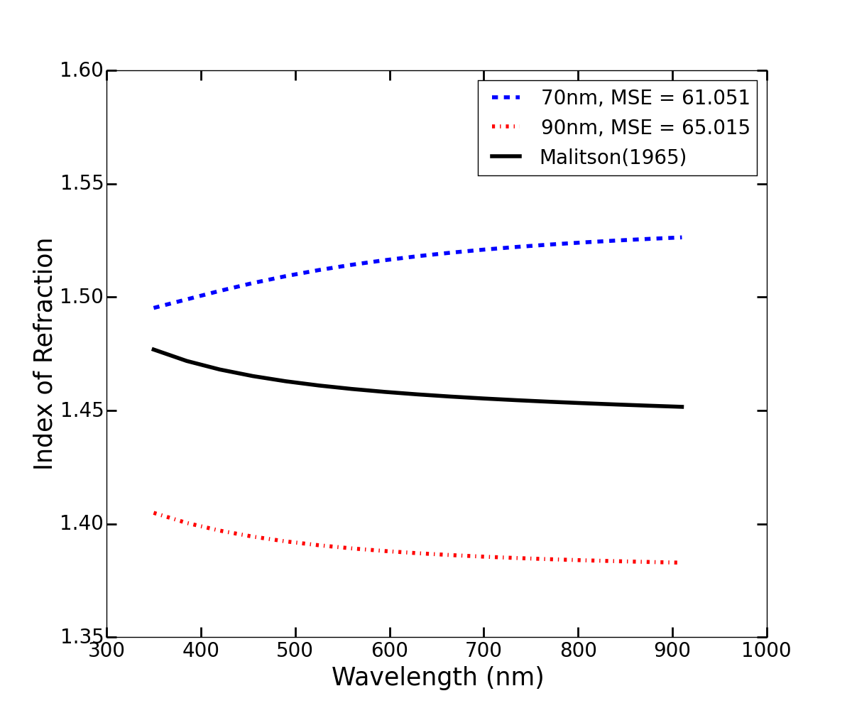
The resultant fits for SiO2 on Si and Ge are shown in Figure 7. The goodness of fit of these curves is demonstrated by the root mean squared error, defined as:
| (8) |
where subscripts and refer to measured and modeled parameters, respectively, and
| number of wavelengths | ||||
The error in the parameters , and that is introduced by the measurements is estimated to be typically 0.001, leading to the extra multiplicative factor of "1000". From equation 8, this implied that a fit with an MSE on the order of unity was considered in "perfect agreement" with the data. Values less than 100 were accepted for our purposes (as suggested by [31]). Fits for HfO2 and TiO2 samples had MSE values greater than 100, and were rejected. This method of testing goodness of fit is done automatically through the CompleteEase software. We found that non-standard coatings require specific calibrations of the ellipsometer. In the future, this will be done in order to characterize the total reflectivity and transmissivity of additional SLAR
7 Predicted Reflectance
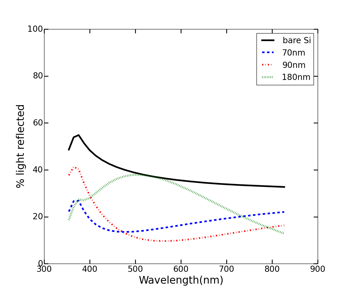
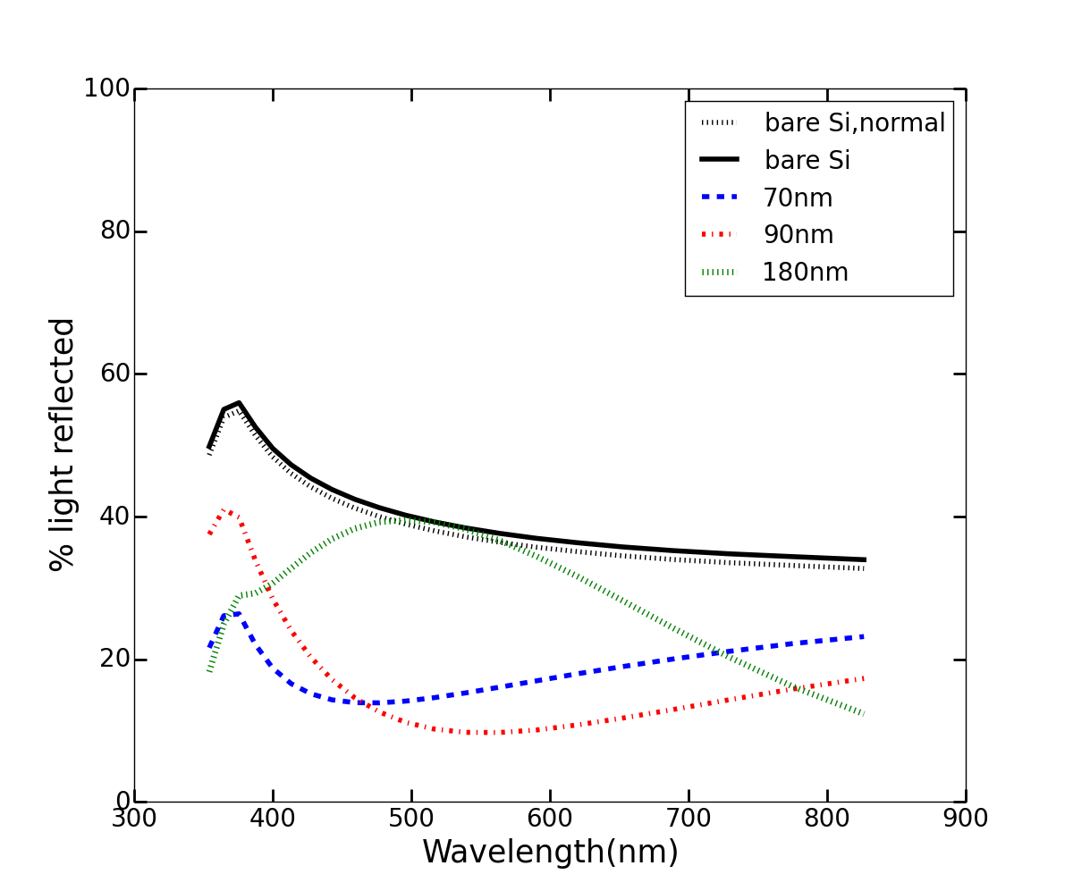
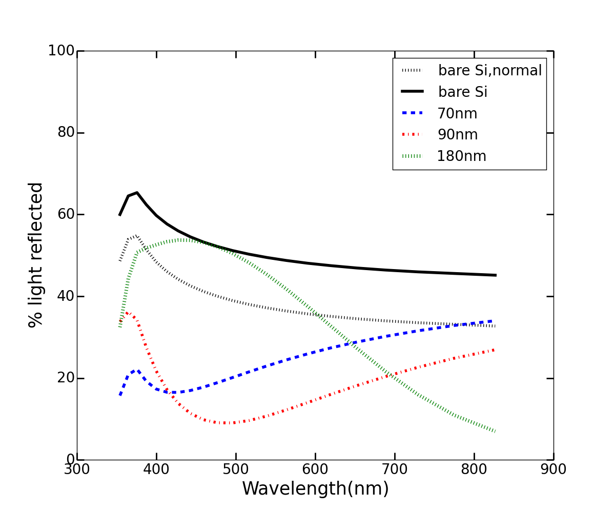
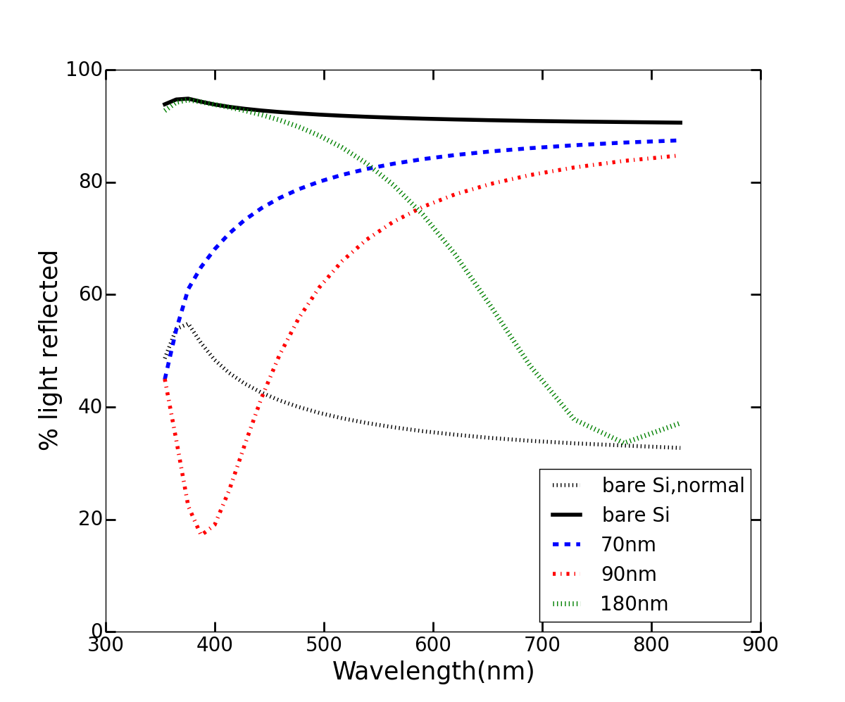
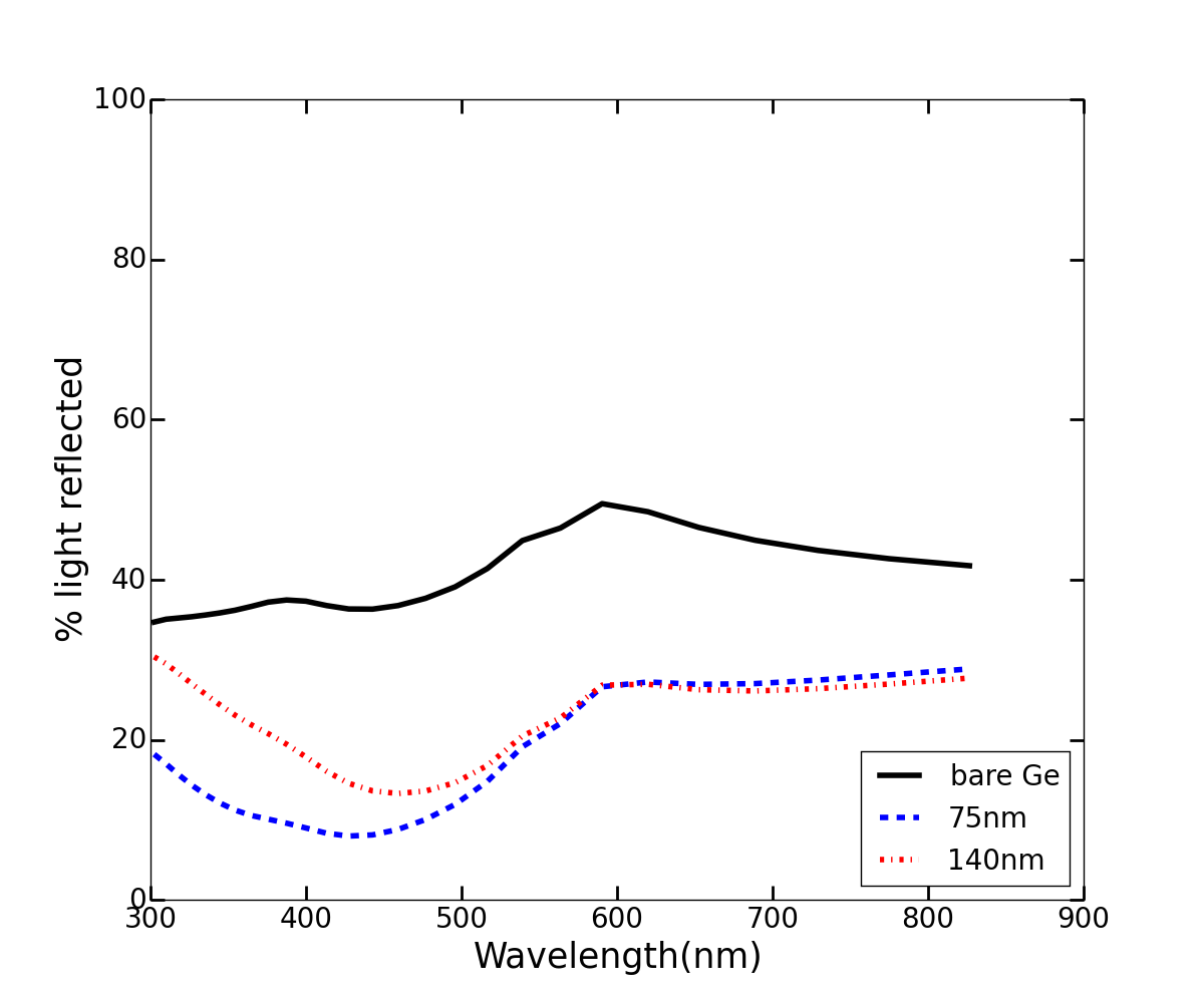
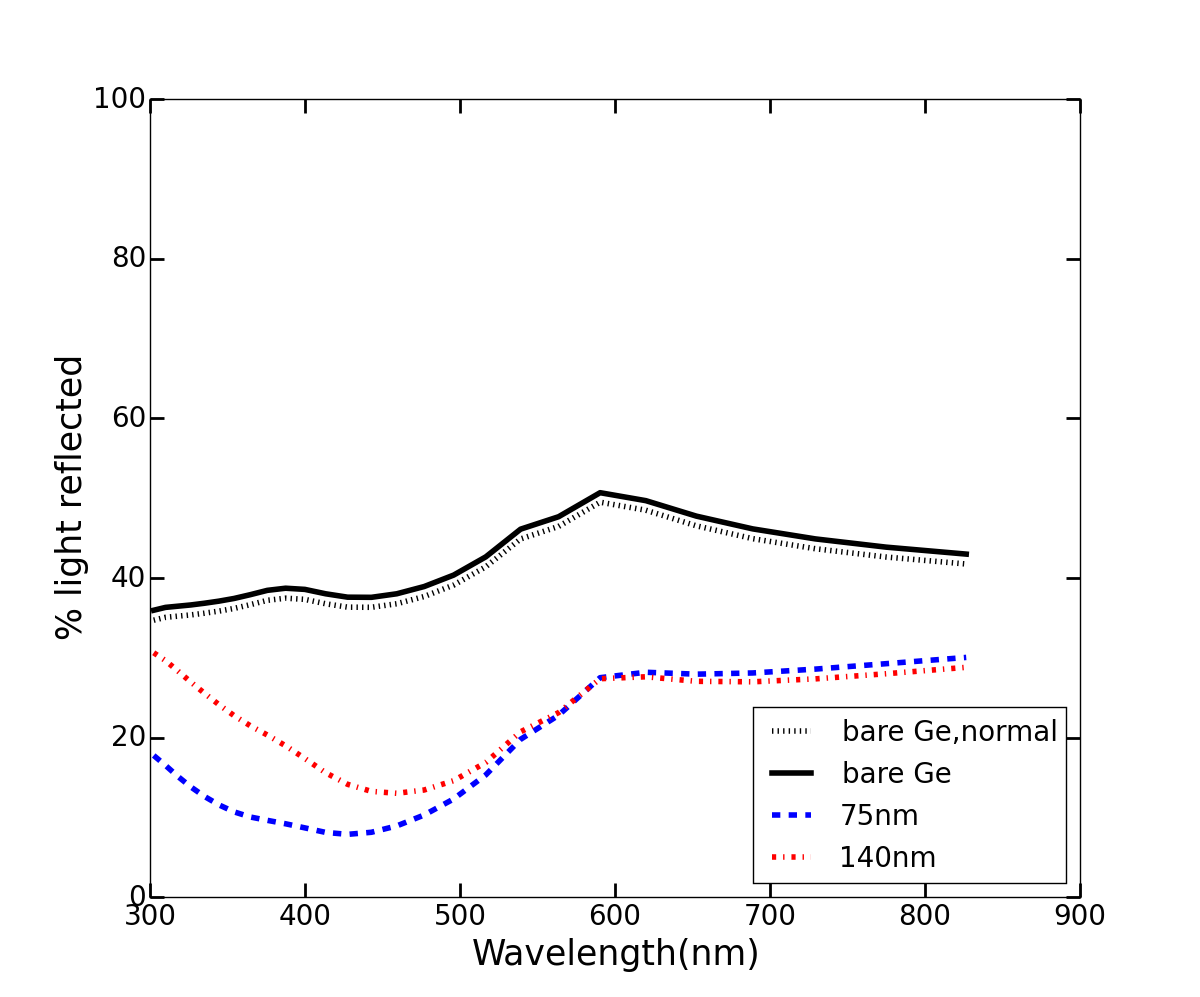
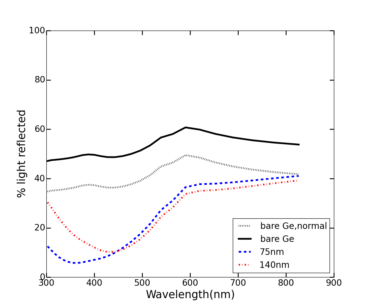
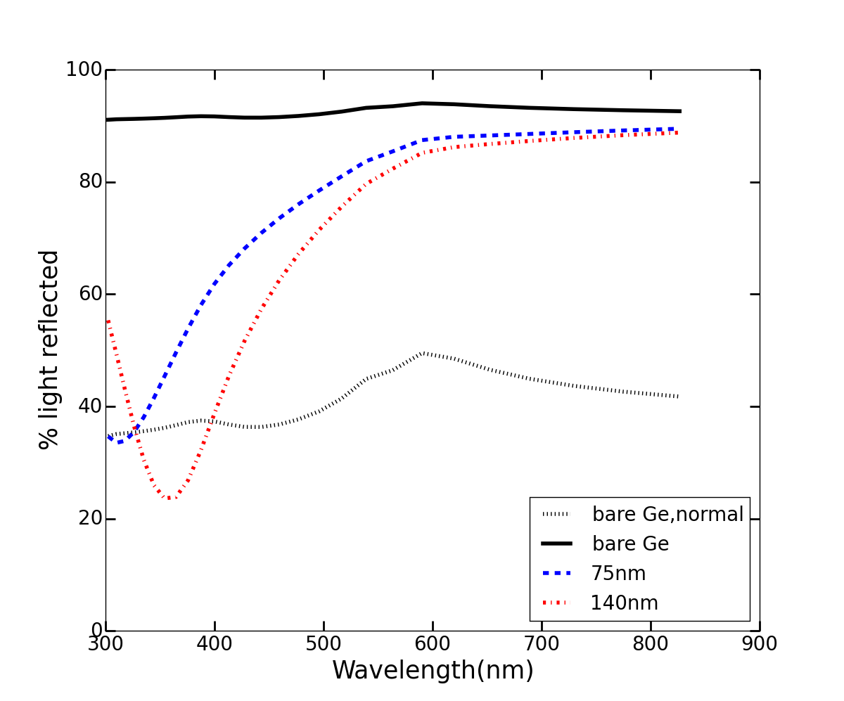
From the indexes characterized in Figure 7, it is possible to reproduce the reflectivity curves for each system. The indices are used as input to equations 1-4 and plotted for various thicknesses and angles of incidence111Incident angles are plotted up to the ellipsometer maximum of 85∘, although calculations suggest the true maximum could be larger.; the results for Si are shown in Figure 8; the results for Ge are shown in Figure 9. All curves are plotted in reference to the reflectance for a bare substrate at normal incidence, and the calculation assumes all reflections are specular and there are no losses in the SLAR ().
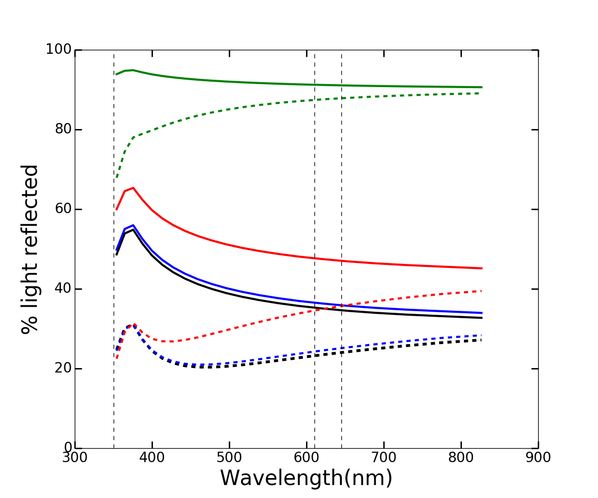
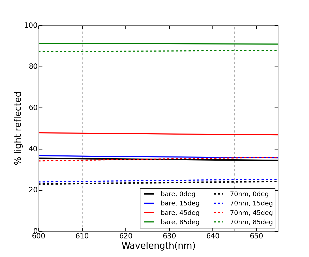
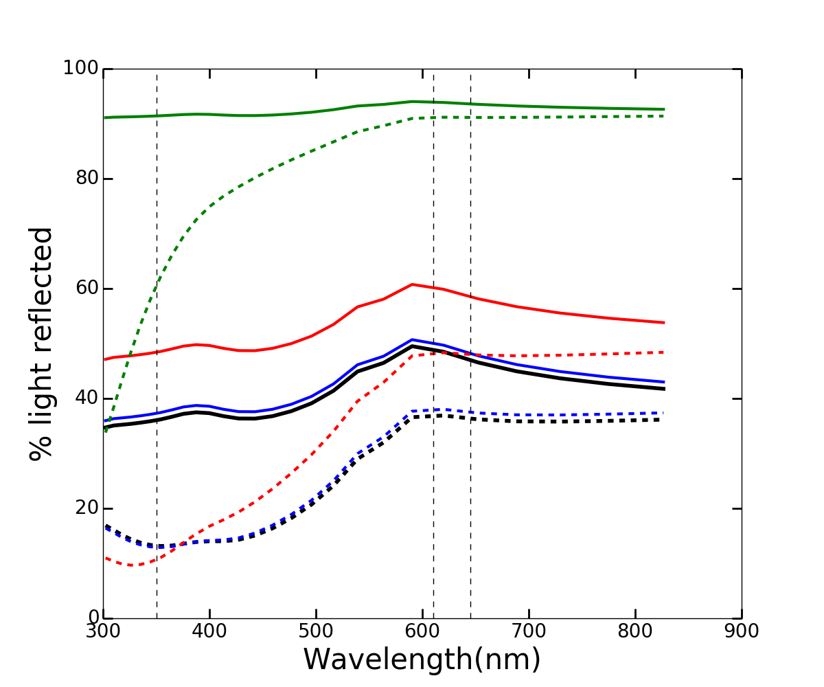
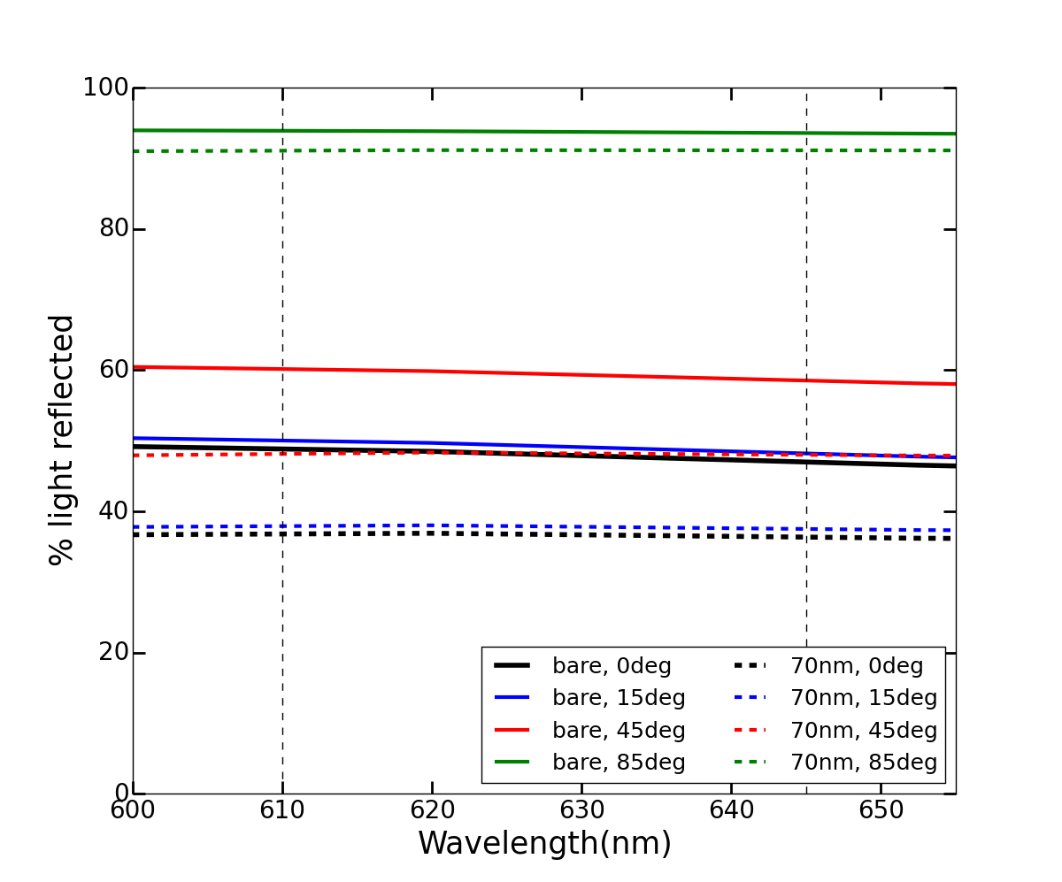
For the peak scintillation wavelengths, 645 nm and 610 nm for ZeSe and ZnMoO4, it is clear that Si substrate reflectivity can be improved with any of the tested SLAR thicknesses: at normal incidence, a 90 nm coating of SiO2 improves reflectivity of an Si substrate by 25%. The performance of the system depends heavily on the film thickness: 180 nm films do not show nearly the same decrease in reflectivity except at higher angles; see Figure 8. In contrast, the Ge substrate performance does not depend as heavily on the SLAR thickness. Improvements of up to 22% were seen for normal incidence for both 75 nm and 140 nm SiO2 coatings on Ge. For the scintillation wavelength of ZnSe (645 nm), the predicted improvement is 20%, which agrees with the findings of previous work [32].
For a signal from Cherenkov light, the solution is quite different. TeO2 has a cutoff wavelength at 350 nm. At this wavelength, it is difficult for a Si substrate to get below 20% reflectivity, so a Ge substrate is a better choice. These results indicate a Ge substrate with a 70 nm SiO2 coating is better than larger thicknesses.
As seen in Figures 8 and 9, results also demonstrate that the performance of these light-collecting, target bolometers is greatly affected by the angle of incident light. Significant amounts of light will be lost simply due to reflectivity: scintillation light incident on Ge from a ZnMoO4 primary bolometer at 45∘ (in the plane of incidence) will be reflected at a 65% loss (see Figure 9(c)). An antireflective coating of 140nm SiO2 can decrease this loss to only about 35%.
8 Conclusion
Anti-reflective coatings can significantly increase the efficiency of light collection bolometers in rare event searches with the purpose of reducing background rates. Several coatings were manufactured successfully on Ge and Si substrates and characterized at room temperature using variable angle ellipsometry. Full characterization of the more rare HfO2 and TiO2 coatings was unsuccessful. Preliminary calculations for both Si and Ge substrates confirm a decrease in reflectivity from SiO2 coatings of various thicknesses at various angles of incidence, an improvement on the calculations performed by [32] which assumed normal incidence. For the ZnSe and ZnMoO4 scintillation wavelengths of 645 nm and 610 nm, coatings of 90 nm SiO2 on Si or 140 nm SiO2 on Ge are recommended. For Cherenkov light from TeO2 at 350 nm, a Ge substrate with a 70 nm SiO2 coating is recommended. Work is ongoing to fully characterize all coatings at operating and room temperatures, as well as to explore the potential of novel coating techniques. Additional analysis of the impact of the coatings on system radiopurity and testing of the coatings characteristic bolometric operating temperatures will fully establish the value of SLAR coatings in rare event searches.
Acknowledgments
This work was funded by the Hellman Fellow program at UCLA. Special thanks to the UCLA NanoLab (Max Ho, Tom Lee, Wilson Lin) and UCSB NanoLab (Tom Reynolds, Brian Thibeault). Many thanks also to Matteo Biassoni, Huan Huang, Jacob Feintzeig, Laura Gladstone, Jon Ouellet, and other CUORE collaborators for their valuable insight and discussion. A special thank you to Laura Gladstone and Jacob Siegel for editing the manuscript.
References
- [1] The CUPID Interest Group, CUPID: CUORE (Cryogenic Underground Observatory for Rare Events) Upgrade with Particle IDentification, 2015.
- [2] G. Angloher, A. Bento, C. Bucci, L. Canonica, X. Defay, A. Erb, F. von Feilitzsch, N. F. Iachellini, P. Gorla, A. Gütlein, D. Hauff, J. Jochum, M. Kiefer, H. Kluck, H. Kraus, J. C. Lanfranchi, J. Loebell, A. Münster, C. Pagliarone, F. Petricca, W. Potzel, F. Pröbst, F. Reindl, K. Schäffner, J. Schieck, S. Schönert, W. Seidel, L. Stodolsky, C. Strandhagen, R. Strauss, A. Tanzke, H. H. Trinh Thi, C. Türkoğlu, M. Uffinger, A. Ulrich, I. Usherov, S. Wawoczny, M. Willers, M. Wüstrich, and A. Zöller, Results on light dark matter particles with a low-threshold CRESST-II detector, The European Physical Journal C 76 (1, 2016) 25.
- [3] M. Kiefer, G. Angloher, A. Bento, C. Bucci, L. Canonica, A. Erb, F. Feilitzsch, N. Ferreiro Iachellini, P. Gorla, A. Gütlein, D. Hauff, J. Jochum, H. Kluck, H. Kraus, J.-C. Lanfranchi, J. Loebell, A. Münster, F. Petricca, W. Potzel, F. Pröbst, F. Reindl, S. Roth, K. Rottler, C. Sailer, K. Schäffner, J. Schieck, S. Schönert, W. Seidel, M. Sivers, L. Stodolsky, C. Strandhagen, R. Strauss, A. Tanzke, C. Türkoğlu, M. Uffinger, A. Ulrich, I. Usherov, S. Wawoczny, M. Willers, M. Wüstrich, and A. Zöller, In-situ study of light production and transport in phonon/light detector modules for dark matter search, Nuclear Instruments and Methods in Physics Research Section A: Accelerators, Spectrometers, Detectors and Associated Equipment 821 (2016) 116–121.
- [4] V. U. o. O. Mikhailik and H. U. o. O. Kraus, Performance of scintillation materials at cryogenic temperatures, 2010.
- [5] S. K. J. Al-Ani, C. A. Hogarth, and R. A. El-Malawany, A study of optical absorption in tellurite and tungsten-tellurite glasses, Journal of Materials Science 20 no. 2 661–667.
- [6] D. E. Aspnes and A. A. Studna, Dielectric functions and optical parameters of Si, Ge, GaP, GaAs, GaSb, InP, InAs, and InSb from 1.5 to 6.0 eV, Physical Review B 27 (1983), no. 2 985–1009.
- [7] GEANT4 Collaboration, S. Agostinelli et al., GEANT4: A Simulation toolkit, Nucl. Instrum. Meth. A506 (2003) 250–303.
- [8] J. Allison et al., Geant4 developments and applications, IEEE Trans. Nucl. Sci. 53 (2006) 270.
- [9] J. Allison, K. Amako, J. Apostolakis, P. Arce, M. Asai, T. Aso, E. Bagli, A. Bagulya, S. Banerjee, G. Barrand, B. Beck, A. Bogdanov, D. Brandt, J. Brown, H. Burkhardt, P. Canal, D. Cano-Ott, S. Chauvie, K. Cho, G. Cirrone, G. Cooperman, M. Cort√©s-Giraldo, G. Cosmo, G. Cuttone, G. Depaola, L. Desorgher, X. Dong, A. Dotti, V. Elvira, G. Folger, Z. Francis, A. Galoyan, L. Garnier, M. Gayer, K. Genser, V. Grichine, S. Guatelli, P. Gu√®ye, P. Gumplinger, A. Howard, I. H≈ôivn√°fçov√°, S. Hwang, S. Incerti, A. Ivanchenko, V. Ivanchenko, F. Jones, S. Jun, P. Kaitaniemi, N. Karakatsanis, M. Karamitros, M. Kelsey, A. Kimura, T. Koi, H. Kurashige, A. Lechner, S. Lee, F. Longo, M. Maire, D. Mancusi, A. Mantero, E. Mendoza, B. Morgan, K. Murakami, T. Nikitina, L. Pandola, P. Paprocki, J. Perl, I. Petrovifá, M. Pia, W. Pokorski, J. Quesada, M. Raine, M. Reis, A. Ribon, A. R. Fira, F. Romano, G. Russo, G. Santin, T. Sasaki, D. Sawkey, J. Shin, I. Strakovsky, A. Taborda, S. Tanaka, B. Tom√©, T. Toshito, H. Tran, P. Truscott, L. Urban, V. Uzhinsky, J. Verbeke, M. Verderi, B. Wendt, H. Wenzel, D. Wright, D. Wright, T. Yamashita, J. Yarba, and H. Yoshida, Recent developments in geant4, Nuclear Instruments and Methods in Physics Research Section A: Accelerators, Spectrometers, Detectors and Associated Equipment 835 (2016) 186 – 225.
- [10] L. Bergé and E. al., Purification of molybdenum, growth and characterization of medium volume ZnMoO 4 crystals for the LUMINEU program, Journal of Instrumentation 9 (2014), no. 06 P06004.
- [11] J. Beeman and E. al., ZnMoO4: A promising bolometer for neutrinoless double beta decay searches, Astroparticle Physics 35 (2012), no. 12 813–820.
- [12] M. Green, Self-consistent optical parameters of intrinsic silicon at 300 K including temperature coefficientss, Solar Energy Materials and Solar Cells 92 (2008), no. 11 1305–1310.
- [13] H. G. Tompkins, A User’s Guide to Ellipsometry. Academic Press, In., San Diego, CA, 1993.
- [14] J. Connolly, B. DiBenedetto, and R. Donadio, Specifications Of Raytran Material, in Proc. SPIE, vol. 0181, pp. 141–144, SPIE, 1979.
- [15] D. M. Chernyak, F. A. Danevich, V. Y. Degoda, I. M. Dmitruk, F. Ferri, and E. N. Galashov, Nuclear Instruments and Methods in Physics Research A Optical , luminescence and thermal properties of radiopure ZnMoO 4 crystals used in scintillating bolometers for double beta decay search, Nuclear Inst. and Methods in Physics Research, A 729 (2013) 856–863.
- [16] N. Uchida, Optical properties of single-crystal paratellurite (TeO2), Physical Review B 4 (1971), no. 10 3736–3745.
- [17] M. Mancuso, J. Beeman, a. Giuliani, L. Dumoulin, E. Olivieri, G. Pessina, O. Plantevin, C. Rusconi, and M. Tenconi, An experimental study of antireflective coatings in Ge light detectors for scintillating bolometers, EPJ Web of Conferences 65 (1, 2014) 04003.
- [18] W. Dash and R. Newman, Intrinsic Optical Absorptionin Single-Crystal Germanium and Silicon at 77K and 300K, Physical Review 99 (1955), no. 4.
- [19] A. Rahman, A. Ashraf, H. Xin, X. Tong, P. Sutter, M. D. Eisaman, and C. T. Black, Sub-50-nm self-assembled nanotextures for enhanced broadband antireflection in silicon solar cells, Nature Communications 6 (2015) 5963.
- [20] N. Coron, P. de Marcillac, J. Leblanc, G. Dambier, and J. P. Moalic, Highly sensitive large-area bolometers for scintillation studies below 100 mK, Optical Engineering 43 (2004) 1568–1576.
- [21] M. Biassoni, C. Brofferio, S. Capelli, L. Cassina, M. Clemenza, O. Cremonesi, M. Faverzani, E. Ferri, A. Giachero, L. Gironi, C. Giordano, C. Gotti, M. Maino, B. Margesin, A. Nucciotti, M. Pavan, G. Pessina, E. Previtali, A. Puiu, M. Sisti, and F. Terranova, Large area Si low-temperature light detectors with Neganov-Luke effect, .
- [22] I. H. Malitson and M. J. Dodge, Refractive Index and Birefringence of Synthetic Sapphire, in J. Opt. Soc. Am., no. 62, p. 1405, 1972.
- [23] D. L. Wood, K. Nassau, T. Y. Kometani, and D. L. Nash, Optical properties of cubic hafnia stabilized with yttria, Applied optics 29 (1990), no. 4 604–607.
- [24] H. R. Philipp, Optical Properties of Silicon Nitride, Journal of The Electrochemical Society 120 (1973), no. 2 295.
- [25] L. Gao, R. Lemarchand, and M. Lequime, Refractive index determination of SiO2 layer in the UV/Vis/NIR range: Spectrophotometric reverse engineering on single and bi-layer designs, Journal of the European Optical Society 8 (2013) 13010–1.
- [26] J. R. Devore, Refractive Indices of Rutile and Sphalerite, Journal of the Optical Society of America 41 (1951), no. 6 416.
- [27] J. W. Fleming, Dispersion in GeO2 SiO2 glasses, Applied Optics 23 (1984), no. 24 4486–4493.
- [28] CUORE Collaboration, C. Alduino et al., The projected background for the CUORE experiment, Submitted to: Eur. Phys. J. C (2017) [arXiv:1704.0897].
- [29] “http://www.universitywafer.com/.”
- [30] “http://www.mtixtl.com/.”
- [31] J. A. Woollam Co. Inc, CompleteEASE Data Analysis Manual, 2008.
- [32] J. W. Beeman, F. Bellini, P. Benetti, L. Cardani, N. Casali, D. Chiesa, M. Clemenza, I. Dafinei, S. Di Domizio, F. Ferroni, A. Giachero, L. Gironi, A. Giuliani, C. Gotti, M. Maino, S. Nagorny, S. Nisi, C. Nones, F. Orio, L. Pattavina, G. Pessina, G. Piperno, S. Pirro, E. Previtali, C. Rusconi, M. Tenconi, C. Tomei, and M. Vignati, Current Status and Future Perspectives of the LUCIFER Experiment, Advances in High Energy Physics 2013 (2013) 1–15.