Robustness of Majorana bound states in the short-junction limit
Abstract
We study the effects of strong coupling between a superconductor and a semiconductor nanowire on the creation of the Majorana bound states, when the quasiparticle dwell time in the normal part of the nanowire is much shorter than the inverse superconducting gap. This “short-junction” limit is relevant for the recent experiments using the epitaxially grown aluminum characterized by a transparent interface with the semiconductor and a small superconducting gap. We find that the small superconducting gap does not have a strong detrimental effect on the Majorana properties. Specifically, both the critical magnetic field required for creating a topological phase and the size of the Majorana bound states are independent of the superconducting gap. The critical magnetic field scales with the wire cross section, while the relative importance of the orbital and Zeeman effects of the magnetic field is controlled by the material parameters only: factor, effective electron mass, and the semiconductor-superconductor interface transparency.
I Introduction
The theory of normal conductor-superconductor (NS) hybrid systems distinguishes two limiting cases: long and short junctions. In long junctions, the dwell time of a quasiparticle inside the normal region is much larger than the time it spends inside the superconductor (with the superconducting gap). In this limit the induced gap inside the semiconductor is equal to , and therefore it varies for different bound states. In the short-junction or strong-coupling limit, the quasiparticles spend most of their time inside the superconductor, while the normal region effectively acts as a delta function scatterer. Then in the presence of time-reversal symmetry, the induced gap is close to for every single Andreev bound state. In the short-junction limit Andreev bound states have the most weight in the superconductor, and therefore the conventional approach of integrating out the superconductor and obtaining an effective Hamiltonian of the normal system becomes inefficient due to the strong energy dependence of the effective Hamiltonian.
Systematically studying the short-junction limit is relevant for the creation of Majorana bound states (MBS) Qi and Zhang (2011); Leijnse and Flensberg (2012); Alicea (2012); Beenakker (2013); Elliott and Franz (2015) in semiconductor nanowiresLutchyn et al. (2010); Oreg et al. (2010) partially coated with epitaxially grown aluminum that have high interface quality. These systems were observed to have a well-developed hard induced gap comparable to the gap in the bare Al Chang et al. (2015), and subsequently showed zero bias peaks Deng et al. (2016) and suppressed splitting of low energy states characteristic to MBS Albrecht et al. (2016). The theoretical description of the response of strongly coupled zero-dimensional NS junctions to magnetic field was analyzed in Ref. Cole et al., 2015, where the authors report a strong suppression of the effective factor, potentially leading to the impossibility of inducing a topological phase at magnetic fields below the Clogston limit Clogston (1962).
Here we extend the analysis of Ref. Cole et al., 2015 using the scattering formalism that allows us to capture the nonlinear features of the spectrum, and by considering higher-dimensional systems with translational invariance. The scattering formalism has been routinely applied to short junctions in mesoscopic physics [Forreviewsee]Beenakker2005. Relevant works to the present study are on two-dimensional electronic gases with spin-orbit interactions Bezuglyi et al. (2002); Dimitrova and Feigel’man (2006). However, in Majorana literature the use of the scattering formalism has been limited Cheng and Lutchyn (2012). The equivalent of the scattering formalism using the effective Hamiltonian approach amounts to introducing an effective self-energy which has a proper dependence on energy Liu et al. (2012); Stanescu et al. (2013); Peng et al. (2015) and then neglecting the energy term in the nonlinear eigenvalue problem , as done in, e. g., Ref. Pöyhönen et al., 2016.
Our overall findings are favorable for the creation of MBS in Al-based NS systems. Specifically, we find that:
-
•
The critical magnetic field required to induce a topological phase is independent of the superconducting gap. This is valid also beyond the short-junction limit, as long as penetration of magnetic field into the superconductor is negligible.
-
•
Since is inversely proportional to the wire cross section, the device design can be used to adjust within a broad range.
-
•
The localization length of the MBS does not depend on the superconducting gap, and in optimal conditions it is proportional to the spin-orbit length .
-
•
Finally, if the interface between the semiconductor and the superconductor has high transparency , then becomes only a slowly varying function of the chemical potential , as opposed to its usual oscillatory behavior on the scale of the mode spacing in the nanowire Wimmer et al. (2010); Lutchyn et al. (2011).
Our analytical calculations fully coincide with the results obtained using a numerical scattering approach to short junctions and exact diagonalization of a discretized tight-binding Hamiltonian. While these conclusions are favorable for the prospect of using weak superconductors for MBS creation, we note that the effects of disorder in the superconductor are not systematically treated here. Disorder has been recently predicted to have a strong detrimental effect on the creation of MBS in systems that are in the short-junction limit Cole et al. (2016).
The paper is organized as follows. Section II contains a pedagogical review of scattering formalism for the calculation of Andreev spectrum. The following Sec. III presents scaling arguments supporting our conclusions. In Sec. IV we compute the dispersion relation of a planar NS junction and discuss the typical device parameters. Section V investigates the Majorana phase diagram and the behavior of the MBS decay length. In Sec. VI we compare the predictions of Sec. V with numerical diagonalization of finite junctions. Section VII estimates the orbital effect of the magnetic field by computing the Andreev spectrum in a cylindrical geometry in a thin shell limit. In Sec. VIII we confirm our findings using a numerically computed Majorana phase diagram of a three-dimensional model. Lastly, section IX sums up our conclusions.
II Scattering matrix formalism and the short-junction limit
This section reviews the scattering approach to calculating the Andreev bound state spectrum and may be skipped by expert readers. We start by considering a general NS junction with superconducting terminals. van Heck et al. (2014) We use the case in Secs. IV, V, VIII and in Sec. VII.
The levels with are Andreev bound states, i.e., coherent superpositions of electron and hole excitations which occur due to Andreev reflections Andreev (1964) at the interface between the normal region and the superconducting terminals. The wave function quantization condition on the wave function requires that the total sequence of scattering events results in a phase shift of . For the vector of modes incoming from the superconductor to the normal region this condition reads:
| (1) |
Here is the scattering matrix of the normal region, and the scattering matrix of Andreev reflection processes in the superconducting terminals. The mode vector has electron and hole components .
The Andreev reflection matrix assumes a universal form when the superconductor has -wave pairing without any sources of time-reversal symmetry breaking and additionally when the Andreev approximation holds (when the Fermi energy in the superconductor is much larger than ). In the literature, the Andreev spectrum is often calculated in systems where the superconductor Hamiltonian has full spin-rotation invariance (an appropriate approximation for aluminum), making the spin basis a natural choice of basis of . Yet the universal structure of the Andreev reflection matrix does not change in the presence of spin-orbit coupling in the superconductor. However, in that case it is impossible to choose a spin basis due to lack of spin conservation and it is more appropriate to use a basis where the outgoing modes are time reversed of the incoming modes Bardarson (2008). Throughout the paper we work in the latter basis but explain the relation to the more commonly used spin basis for reference at the end of this section. Importantly, we neglect the time-reversal symmetry breaking perturbations in the superconductor, restricting ourselves to magnetic fields much lower than critical.
The scattering matrix of the normal region is block diagonal in the Nambu space:
| (2) |
where and are the scattering matrices of electrons and holes. We consider NS junctions with a translational symmetry, and therefore the scattering matrices may depend on the wave vector along the translationally invariant directions. We choose the hole modes as particle-hole partners of the electron modes . In this basis the particle-hole symmetry of the scattering matrix reads:
| (3) |
Using the block-diagonal structure of it follows that the normal scattering matrix of holes is the conjugate of the scattering matrix for electrons, at opposite energy and momentum Beenakker (2015):
| (4) |
In the same basis, the Andreev reflection matrix reads:
| (5) |
where the index runs over the terminals, is the superconducting phase in lead , and . Beenakker (1991)
Following Ref. Beenakker, 1991, eliminating from Eq. (1), and using an expression for a block matrix determinant one immediately arrives to a determinantal equation for the bound state energies:
| (6) |
The short-junction limit allows us to further simplify the calculation of the Andreev bound state energies when Thouless energy . Thouless energy is the typical energy scale for the matrix elements to change appreciably, therefore in the short-junction limit for any . After replacing with , the only energy-dependent term remaining in Eq. (1) is the coefficient . Since the scattering matrices are invertible, Eq. (1) reads:
| (7) |
Adding the two equations yields the following energy eigenproblem:
| (8) |
Further squaring this equation and using the unitarity of the scattering matrices and we arrive to the eigenproblem expression for the Andreev spectrum:
| (9) |
where the energy argument is suppressed, since is evaluated at . If there is only a single superconducting terminal, the Andreev reflection matrix reduces to a phase factor, which fully drops out from Eq. (9), as required by gauge invariance.
If the spin is conserved, the above derivation is nearly identical in the spin basis. The scattering matrices in the spin basis and are related to the basis of time-reversed modes by a transformation
| (10) |
with the Pauli matrices spin operators and an identity matrix. The symmetry condition (4), equation (6) for the Andreev spectrum, and eigenproblem for the spectrum in short-junction approximation (9) are identical in both bases upon replacing and with and .
III Scaling arguments for the MBS properties in the short-junction limit
The superconducting gap enters only as an overall prefactor of the Andreev state energies in Eq. (9), while the specific spectrum depends only on the normal state scattering matrix . This simplification allows us to draw most of our conclusions about MBS properties solely using universal arguments and not by solving a specific model. For instance, since the Majorana phase transition occurs when Eq. (9) has a zero-energy solution, the critical field does not depend on . This conclusion also extends beyond the short-junction limit, since the zero energy solutions of Eq. (9) always coincide with the zero energy solutions of the Eq. (1) and therefore with the full solutions of the Bogoliubov-de-Gennes equation.
Turning to the spatial extent of MBS in the normal region , we observe that it is limited from below by the coherence length in the superconductor. However is often short: For example in aluminum films due to disorder effects. If is predominantly set by the properties of induced superconductivity in the normal region, must also be independent of , since it is a property of the eigenvectors of Eq. (9) at .
If the semiconductor has a cross section , effective electron mass , and it is coupled to the superconductor by an interface with transparency , then the Thouless energy equals
| (11) |
where is the number of transverse bands occupied in the semiconductor, and is the typical interband spacing. The denominator of the expression for contains since it is the total distance traveled by a quasiparticle normal to the interface between two consecutive Andreev reflections. We focus on the experimentally relevant low-density regime when . In realistic nanowires , and , resulting in , much larger than the superconducting gap in aluminum , which justifies the short-junction approximation for sufficiently transparent contacts .
In order for the spectral gap to close in the normal region—or, in other words, for a topological phase transition to appear—the scattering matrix must change by since, in the presence of time-reversal symmetry, all the Andreev bound states have the same energy . For the Zeeman field to cause such a perturbation, the electron spin must precess by a large angle during the propagation inside the scattering region. This results in a condition , or equivalently
| (12) |
with the effective gyromagnetic factor and the Bohr magneton.
The orbital effect of the magnetic field causes an additional time-reversal symmetry breaking perturbation to the normal scattering region. It becomes significant [causes an change of ] when the flux penetrating the scattering region becomes comparable to the flux quantum . This defines another scale of the magnetic field, characterizing the importance of its orbital effect . Comparing with we get
| (13) |
If transparency is high and the number of modes is low, then the relative strength of the orbital and Zeeman effects of the magnetic field is a material parameter dependent on the factor and the effective mass. For realistic materials this factor is , which is in line with our results in Secs. VII and VIII.
Turning to the spatial extent of the MBS , we observe that it must diverge in the topological regime in the absence of spin-orbit coupling. The spectral gap at a finite momentum appears already in the first order perturbation in spin-orbit strength , and hence . Finally, in the optimally tuned situation , and , so that only depends on two energy scales: and the spin-orbit energy . This means that there is only a single length scale inversely proportional to , the spin-orbit length , and hence .
The scattering approach highlights another important property of the Majorana phase diagram, the relation between and the oscillatory behavior of . If , there is little scattering at the NS interface, and becomes a smooth function of the chemical potential . Combining this with Eq. (12) we conclude that must also depend on in a smooth fashion. In the opposite limit , reduces on resonance, when matches the bottom of a subband in the semiconducting region. Away from the resonance, when there are no available states at the selected energy, becomes very large. This behavior of Thouless energy results in the appearance of a sharp minimum in whenever matches the bottom of a new band in the semiconductor region. In Sec. IV we confirm the relation between the interface transparency and the oscillatory nature of the Majorana phase boundary.
These findings are different from the predictions of a purely 1D phenomenological model Lutchyn et al. (2010); Oreg et al. (2010) with the Hamiltonian
| (14) |
where the induced superconductivity enters as a phenomenological pairing term , and the momentum is limited to a direction along the nanowire. The induced gap follows from a perturbation theory in the weak coupling limit between the semiconductor and the superconductor. Therefore the phenomenological model is not directly applicable to the strong coupling regime for highly transparent junctions. The Hamiltonian undergoes a topological phase transition when , and therefore explicitly depends on . This difference, however, is due to the shortcomings of the effective model, and in reality our conclusions also hold in the weak-coupling/long junction limit. In the long junction limit , immediately leading us to the conclusion that and are independent of the intrinsic superconducting gap . If a long junction is transparent , then the Fermi momentum drops out of the level quantization condition, hence resulting in the lack of oscillations of as a function of . Finally, the rest of our conclusions follow in a similar fashion for the long junctions from the dimensional analysis of Eq. (14) after the identification .
IV Model
IV.1 General solution
To verify our general arguments, we consider a specific model, a semiconductor nanowire in contact with a large superconductor. We consider the effective superconductor thickness to be infinite, unlike the typical experimental situation where the superconductor thickness is around . This limit is nevertheless a reasonable approximation due to the large Fermi surface size mismatch between the superconductor and the semiconductor. A much larger Fermi surface in the superconductor means that most electron trajectories approaching the nanowire from the superconductor side must be reflected back. Full internal reflection in combination with diffuse scattering allows the superconductor to accommodate quasiparticle trajectories much longer than the superconducting coherence length , making the superconductor effectively infinite.
We first consider the device geometry shown in Fig. 1. The nanowire is oriented along the axis, NS interface is at , and the outer boundary of the wire is at . The superconductor occupies the half-space . Neglecting the orbital effect of the magnetic field makes the motion in direction separable and reduces the problem to a purely two-dimensional geometry, shown in Fig. 1(b).
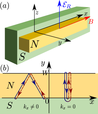
The normal state Hamiltonian of the system is that of a Rashba two-dimensional electron gas coupled to a material with negligible spin-orbit interaction and Zeeman coupling BenDaniel and Duke (1966):
| (15) |
Here are the spin Pauli matrices, and the momentum operator. The chemical potential and effective mass are
| (16) |
Additionally, we neglect the spin-orbit coupling and the magnetic field effect in the superconductor, therefore restricting the model to , with the critical field of the superconductor:
| (17) |
with the Heaviside step function and , the Rashba spin-orbit coupling strength. The spin-orbit term in Eq. (15) is symmetrized using anticommutators to ensure current probability conservation at the interface. The Zeeman energy is due to a magnetic field of magnitude oriented along the wire direction. The effective electric field generating the Rashba spin-orbit coupling is . To compare the short-junction approximation with exact diagonalization results, we use the Bogoliubov-de Gennes (BdG) Hamiltonian:
| (18) |
with . The choice of a step-function pairing potential is justified due to a density of states mismatch between the superconductor and semiconductor by more than , which renders the self-consistency condition on unimportant.
To make further analytical progress, we neglect the spin-orbit coupling in the direction . This is a valid simplification since in semiconductor nanowires the spin-orbit length is usually larger than the nanowire width . We later verify the validity of this approximation by computing the exact expression for the topological phase boundary and by including the transverse spin-orbit coupling in all the tight-binding simulations.
The wave function in the nanowire satisfies the boundary condition and has the general form
| (19) |
with
| (20) | |||||
and unknown amplitudes. The wave function in the superconducting lead has the form
| (21) |
with the amplitudes of the incoming modes, the amplitudes of the outgoing modes, and the relative signs chosen to ensure that the incoming and outgoing modes are time-reversed of each other. Finally, the momenta and normal to the NS interface are fixed by the dispersion relation at energy :
| (22) |
We use the wave function continuity at as well as the current conservation condition on the wave function derivative normal to the interface, in the direction:
| (23) |
Solving for and for given we obtain the scattering matrix:
| (24) |
with the reflection phases of different spin projections given by
| (25) |
Here we introduced the transverse velocities in the superconductor lead and in the nanowire.
The scattering matrix holds generally at energies below the superconducting gap . In the short-junction approximation, is evaluated at Fermi energy . Then the Andreev bound spectrum follows immediately upon solving the eigenvalue problem (9):
| (26) |
This dispersion relation admits no zero energy solutions for and . The parameters values yielding are the topological phase transitions, and they occur when
| (27) |
In the derivation of the Andreev spectrum (26) we neglected the effect of spin-orbit interactions in the direction since . For completeness, we analyze the impact of this spin-orbit coupling on the condition for gap closing at . In the presence of transverse spin-orbit coupling, one needs to take into account the Hamiltonian (15) including the term. Then the boundary condition at the NS interface needs to be modified in order to ensure the current conservation. Integrating the Schrödinger equation near the interface yields:
| (28) |
Since at , the Hamiltonian (15) commutes with , the scattering states in the semiconductor region are also eigenstates of . Matching the wave functions at the NS interface and solving the scattering problem results in a condition for closing the excitation gap identical to Eq. (27), but with the modified scattering phases (25):
| (29) |
For our parameter choice , and is more than two orders of magnitude smaller than . This confirms that spin-orbit dynamics in direction is negligible.
IV.2 Typical physical parameters of the heterostructure
To consider a specific example of the system parameters we take InSb nanowires Mourik et al. (2012) with effective mass (here is the free electron mass), and with spin-orbit length . The superconductor in the heterojunction is aluminum, with and chemical potential . A thin Al film has the bulk superconducting gap and the critical magnetic field that varies from around to .
While most of our results scale trivially with , we choose whenever it is necessary to compare the magnetic field or chemical potential scales to the experimental parameters. This results in , well within the requirements of the short-junction approximation.
IV.3 Modeling the NS interface
The final crucial parameter of the hybrid system is the transparency of the NS interface. In the model Hamiltonian (15) the interface properties are set by the velocity ratio , the only way the superconductor Hamiltonian parameters enter the scattering matrix (25). We use the as a free parameter allowing us to study the effect of the interface properties on the topological phase diagram.
While the Fermi energy difference between aluminum and the semiconductor may span several orders of magnitude, the Fermi velocities do not differ so much because of a smaller effective mass in narrow band semiconductors. Specifically, the Fermi velocity in aluminum is , while at a relatively low , resulting in . In real systems, the microscopic interface properties such as coupling strength and charge accumulation further influence the interface transparency. In the absence of a Schottky barrier, extra charge density at the interface smoothens the sharp change in velocity between the semiconductor and the superconductor and further enhances the transparency.
Transparency of the NS interface is hard to measure experimentally due to the complicated geometry of the normal metal-nanowire-superconductor samples. The experiments using high superconductors such as NbTiN are in a long junction regime allowing us to estimate because the induced superconducting gap is . On the other hand, tunneling spectroscopy only provides a lower bound on the transparency: in the short-junction regime.
To explore the impact of interface transparency on the MBS properties we adopt two choices of : the highly transparent interface corresponding to and an interface with a finite transparency where we fix the value of to a constant. For convenience we choose an anisotropic mass in the superconductor , , so that results in a perfect transmission at a and . The condition ensures that only weakly depends on , as it should due to the Fermi surface in the superconductor being much larger than in the semiconductor. In most calculations we use , however our conclusions are not sensitive to this choice (see Appendix A for details).
Adapting the calculations of Sec. IV.1 to the case of anisotropic mass and transparent limit yields the same result for the excitation spectrum (26), up to replacing the transverse momentum in the superconductor with
| (30) |
IV.4 Comparison with tight-binding dispersion simulations
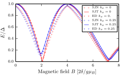
To verify the correctness of the spectrum in the short-junction limit, Eq. (26), we compare the analytical expressions with dispersion relations calculated using a Hamiltonian (15) discretized on a square lattice with lattice constant and simulated using Kwant packageGroth et al. (2014). We first numerically obtain the scattering matrix of the normal region and use it as an input to Eq. (9) to obtain the dispersion relation of the hybrid system.
A further comparison is provided by modeling the hybrid system using the full BdG Hamiltonian (18) and calculating several eigenstates closest to the Fermi level. In this case, the junction remains infinite along the wire, but instead of a superconducting lead, we attach a large superconductor with width .
A comparison between analytics and the two numerical methods at a fixed chemical potential is shown in Fig. 2 and shows nearly perfect agreement between different methods. Slight deviations of exact diagonalization results occur near the bulk gap, caused by corrections to the short-junction approximation.
V Analysis of the topological phase diagram
V.1 Phases boundaries and the spectral gap
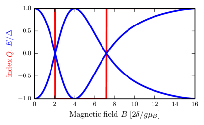
Equation (27) yields the closing of the spectral gap and the topological transitions in the model. This allows us to define the topological invariant of the Hamiltonian as
| (31) |
where the sign of the square root is fixed by the analytic continuation and chosen such that in the trivial state. A typical spectrum at as well as for a fixed is shown in Fig. 3.
In addition to identifying the topological phase boundaries for each set of parameters we calculate the spectral gap
| (32) |
with given by Eq. (26). The minimization is carried over all present in the superconductor. In general, the dispersion relation has several local minima, as shown in Fig. 4, with the total number of minima approximately equal to the number of transverse modes in the normal region.
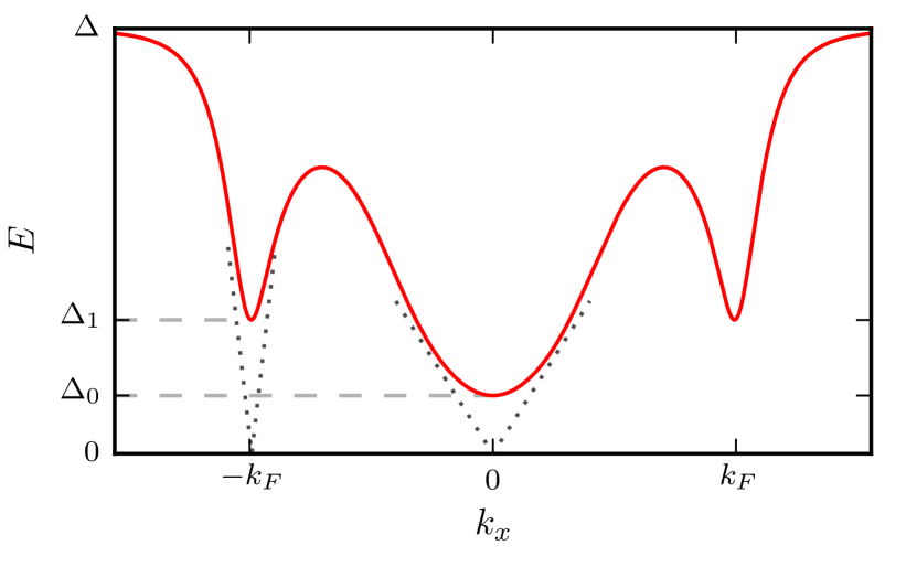
The resulting topological phase diagram of a transparent junction (with ) is shown in Fig. 5. For typical junction parameters (as described in Sec. IV.2) , and the phase diagram for higher field values does not apply to such junctions. The minimal value of the critical field in this phase diagram corresponds to . Near the topological phase transitions , the spectral gap at (see Fig. 4), and it varies linearly with the distance from the phase transition either along the or axis:
| (33) |
Deep in the topological phase, is limited by the gap at (see Fig. 4), similar to the phenomenological model of Eq. (14). Since must vanish linearly with in this regime, we get
| (34) |
In both estimates we assumed , and . Comparing Eqs. (33) and (34) we find the energy scale for the transition between the two behaviors .
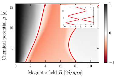
The most unusual feature of the topological phase diagram in Fig. 5 is the smooth behavior of the topological phase boundary, different from the hyperbolically-shaped boundary of the phenomenological modelsLutchyn et al. (2010); Oreg et al. (2010); Lutchyn et al. (2011). This difference appears not due to the short-junction limit—since the magnitude of the gap does not impact the topological phase boundary—but rather because of the high interface transparency. The inset in Fig. 5 shows the shape of the topological phase boundary where we have reduced the transparency by fixing at a high value. We find that in this case the phase boundary has a hyperbolic shape predicted by the phenomenological model.
V.2 Decay length of MBS
Exact evaluation of the MBS decay length starting from Eq. (26) is not possible because the spectrum in the short-junction approximation does not correspond to a local Hamiltonian (the same fact manifests in the complex nonlinear dispersion of the Andreev states). Nevertheless, the decay length is approximated well by assessing the contributions of different local minima of the dispersion relation, as shown in Fig. 4. A gapped Dirac cone with velocity and gap results in a wave function decay length at . The size of the MBS is set by the slowest decaying component of the wave function, or the largest .
Once again, it is instructive to estimate using scaling arguments in two regimes: near a topological transition and deep in the topological phase. At the phase transition point the slope of the Dirac cone at , since without spin-orbit coupling the band touching at must have a parabolic shape. Since the bulk superconductor gap must enter the spectrum only as an overall prefactor, we get
| (35) |
The velocity at the outermost Dirac point must not depend on , resulting in
| (36) |
The two length scales and become equal at .
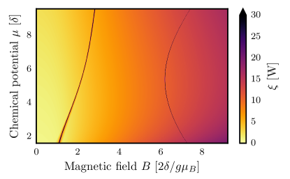
We obtain the behavior of in the tight-binding simulations using Kwant Groth et al. (2014) for the same parameters as in Fig. 5. In order for the self-energy to become local in the coordinate we neglect the transverse dispersion in the superconductor and set . We then integrate out the superconductor and add a self-energy to the semiconductor. Finally, similar to Ref. Nijholt and Akhmerov, 2016 we perform an eigendecomposition of the translation operator in the direction at zero energy to obtain the evanescent waves , with the eigenvalue of the translation operator. The largest decay length is:
| (37) |
where the maximum is taken over all the eigenvalues. Then in the topological phase . The results are presented in Fig. 6. The divergence in decay lengths seen in Fig. 6 corresponds to topological transitions identical to the ones found in Fig. 5. Figure 6 also confirms that saturates at a distance away from that phase transition (here ).
We now refine the scaling arguments of Eqs. (35) and (36) by using Eq. (26). In particular, near the topological transition, the decay length is determined by the spectral gap and the velocity :
| (38) |
with Fermi velocity
| (39) |
Therefore the MBS decay length is inversely proportional to the magnetic field and spin-orbit length near the Majorana phase transitions.
Deep in the topological phase it is more difficult to obtain a closed form approximation for the decay length. Instead, we find the Fermi momentum and the spectral gap by performing numerical minimization of the energy dispersion (26). The Fermi velocity near follows immediately:
| (40) |
Taking the ratio (36), it follows that the MBS decay length does indeed grow linearly with magnetic field and spin-orbit length deep in the topological phase [see Fig. 7], in qualitative agreement with the numerical calculation using Eq. (37).
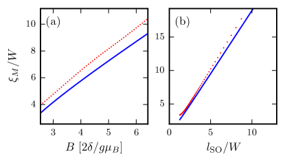
Our results for the scaling of with and agree with the predictions of the phenomenological 1D model both near the topological transition or deep in the topological phase (see, e. g., Ref. Klinovaja and Loss, 2012), but we find no dependence of on .
VI Spectrum of finite length junctions
To directly verify the existence of a MBS and the applicability of the short-junction limit to our system, we solve the discretized BdG Hamiltonian of a large rectangular system with a finite superconductor. The system is divided into semiconductor and superconductor regions, both modeled by the BdG Hamiltonian (18). The length of the system is , sufficiently long to ensure that the overlap between MBS is small. Further, we choose the width of the superconductor sufficiently large . The lattice constant in the tight-binding simulation is . Finally, the remaining model parameters are chosen according to Sec. IV.2 and Sec. IV.3. We determine numerically several lowest energy states and compare them with calculated in Sec. V, as shown in Fig. 8.
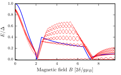
We observe that the energy of most subgap states is bounded from below by an energy slightly lower than , as expected close to the short-junction regime. At the system enters a topological regime and states with formed by two coupled MBS appear. The coupling of these states decays exponentially with the size of the nanowire . Finally after the system undergoes the second gap closing and enters the trivial phase at additional low energy states appear due to the presence of chiral symmetry of the Hamiltonian (15) Schnyder et al. (2009); Ryu et al. (2010); Tewari and Sau (2012). We therefore conclude that our calculations fully apply to finite nanowires in the short-junction regime.
Furthermore, we verify in Appendix B using exact diagonalization that the critical field is indeed independent on the superconducting gap . With increasing above the system exits the short-junction regime. Nevertheless, the critical magnetic field stays constant, in agreement with the proof of Sec. III.
VII Orbital field effect in thin shell approximation
We now turn to evaluate the consequences of the orbital effect of the magnetic field, known to strongly influence MBS properties Lim et al. (2013); Osca et al. (2014); Osca and Serra (2015); Nijholt and Akhmerov (2016), in the short-junction limit. This effect does not manifest in the model of Sec. IV when magnetic field points in the direction. To include the orbital effect we use a thin shell approximation, when the electron wave function in the semiconductor is confined to its surface, similar to the system studied in Ref. Osca et al., 2014. However unlike Ref. Osca et al., 2014 we do not assume a constant induced gap and consider instead the nanowire contacted by a bulk superconductor, as shown in Fig. 9. We model the coupling to the superconductor as two infinite planar superconductors on each side of the 2D uncovered wire section. By doing so we neglect the possibility for electrons to tunnel through the superconductor to the other side of the uncovered section, which is justified by the density mismatch between the superconductor and the semiconductor. The thin shell limit is oversimplified and it overestimates the orbital effect of a magnetic field, however it provides an upper bound on the impact of the orbital effect and remains analytically tractable.
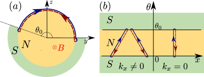
The superconductor covers the wire over an angle , while both the wire and the superconductor are translationally invariant in the direction. In cylindrical coordinates the electron Hamiltonian on the nanowire surface reads:
| (41) |
with , and the radius of the nanowire. We assume that the magnetic field is fully screened from the superconductor and choose a gauge where the vector potential in the uncovered part of the surface, while the two superconducting leads have a phase difference . Compared to the previous sections where the treatment was more general, we assume from the start the transparent junction limit, when Fermi velocities at are identical in the superconductor and the semiconductor and we also neglect the spin-orbit coupling in the transverse direction, as appropriate for .
We solve the scattering problem in the basis of conserved spin projections set by Eq. (20) corresponding to the basis of incoming and outgoing modes:
| (42) |
with and the amplitudes of incoming and outgoing modes, denoting the modes at , the modes at , and superscript corresponding to the two conserved spin directions (20). For each spin projection the scattering matrix is given by the classic result for transmission through a potential barrier:
| (43) |
with
| (44) |
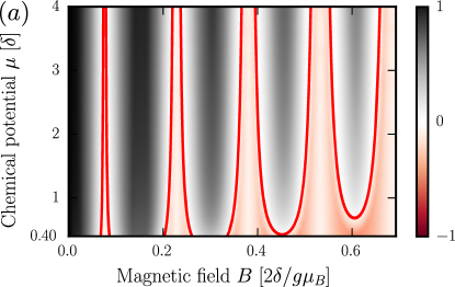
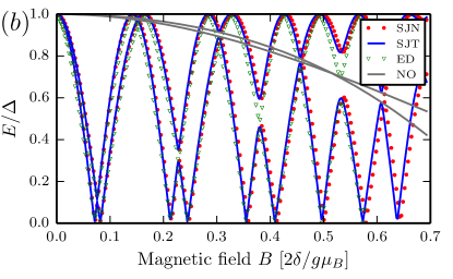
with momenta and defined by Eq. (30). We then transform the scattering matrix to the basis of time-reversed modes (21) and calculate the Andreev spectrum using Eq. (9) with the phases of superconducting leads equal to and . We verify again that the dispersion relation obtained this way agrees well with two numerical tight-binding simulations at fixed chemical potential and that the difference also stays small if we include spin-orbit coupling in the transverse direction [see Fig. 10(b)]. As before, the spectrum is generically gapped except at , where topological phase transitions occur.
The resulting Majorana phase diagram is shown in Fig. 10(a), and it consists of several narrow topological regions centered around with integer. At these values of magnetic field, the two superconducting leads have a phase difference of , thus fully suppressing the induced gap in the transparent limit. The Zeeman field then opens a topological gap resulting in a finite extension of the topological phases around . We conclude that in the thin shell limit, the orbital effect of the magnetic field reduces by a factor for typical junction parameters (we once again note that the thin shell limit overestimates the orbital effect of the magnetic field). Despite that, it is the Zeeman field responsible for opening the topological gap.
VIII Numerical study of a three-dimensional nanowire
To confirm our findings in a model with a more realistic geometry, we numerically calculate the phase diagram of a three-dimensional nanowire in the short-junction limit. The system consists of a semiconductor nanowire infinite in the direction and with a square cross section contacted by a bulk superconductor occupying half space [see Fig. 1(a)].
Due to the large Fermi surface mismatch between the superconductor and the semiconductor we neglect the electron dispersion in the and directions in the superconductor. Therefore, following Sec. IV.2 we set and . Since the semiconductor modes with different values of have different interface transparencies, we cannot ensure a transparent interface for all the modes and instead fix while varying . The remaining system parameters are specified in Sec. IV.2.
The model Hamiltonian is a three-dimensional generalization of Eq. (15) discretized on a cubic lattice. We include the orbital effect of the magnetic field using Peierls substitution in the gauge . This ensures that the vector potential is constant in the direction and that it vanishes at the interface with the superconductor.
We calculate the excitation spectrum using Eq. (9) to find by minimization over . The resulting phase diagram of is shown in Fig. 11. Comparing the top panels of Fig. 11 with Fig. 5 we observe the two sharp minima of . These correspond to the appearance of the additional bands with a different value of and a minimum in the interface transparency. 111The code for the tight-binding simulations of the two-dimensional and three-dimensional junctions is available in ancillary files to the manuscript.
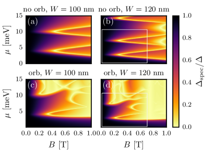
Similar to our observations from Sec. VII, the orbital effect of the magnetic field has a strong effect on the shape of the topological phase boundaries and reduces both and similar to the thin shell simulations. Increasing the cross section of the wire [Fig. 11(a), (c), against (b), (d)] confirms that in 3D the critical fields preserve the scaling with independent of the presence or absence of orbital effects.
IX Conclusions and outlook
We have studied the impact of a small superconducting gap on the properties of MBS in semiconductor-superconductor junctions. The short-junction formalism, appropriate for this limit, allows us to draw universal conclusions about the MBS properties. Contrary to the intuitive expectations, we show that the reduction of the superconducting gap does not alter the Majorana phase diagram and does not change the size of the MBS. We therefore conclude that in most practical systems the superconducting gap should not be used as an important parameter in optimizing MBS properties.
On the other hand, we find that the transparency of the semiconductor-superconductor boundary has an important and previously overlooked effect on the Majorana phase diagram. An interface with produces a phase boundary between trivial and topological phases which depends weakly on the chemical potential. This is in contrast to , used in most prior research, that results in the critical magnetic field having an oscillatory dependence on chemical potential with minima corresponding to the opening of a new band.
Orbital effect of magnetic field plays a dual role: It reduces the critical magnetic field as well as the spectral gap in the topological regime. Contrary to the predictions of a phenomenological model that assumes a constant induced gap, we show that relative importance of magnetic field cannot be controlled by the superconducting gap or the diameter of the nanowire.
Our findings suggest that creation of MBS in proximitized two-dimensional electron gases laterally contacted by a superconductor is a promising direction of further research. In these systems the relative strength of the orbital and the Zeeman effect of magnetic field is controlled by an extra tuning parameter: the ratio between the semiconductor thickness and its width. Additionally, the critical magnetic field in such devices could be tuned using a side gate, effectively changing the semiconductor width without altering the superconductor-semiconductor interface transparency.
Another important further direction of research is the interplay between junction transparency and disorder. Since a transparent interface results in a weaker dependence of the critical magnetic field on the chemical potential, it is reasonable to conjecture that the sensitivity of MBS properties to disorder is also reduced in the transparent regime.
Acknowledgements.
The authors thank B. van Heck, M. Irfan, M. P. Nowak, T. Ö. Rosdahl, and M. Wimmer for many fruitful discussions. This research was supported by the Foundation for Fundamental Research on Matter (FOM), the Netherlands Organization for Scientific Research (NWO/OCW) as part of the Frontiers of Nanoscience program, and an ERC Starting Grant.Appendix A Interface transparency in a two-dimensional junction
The validity of the short-junction approximation depends on NS interface transparency . In this section, we review the transparency of a sharp interface between two materials with a parabolic dispersion. We provide quantitative arguments for the choice of anisotropic mass in the superconductor in modeling a transparent interface.
We consider a planar NS interface with the boundary located at , and both materials occupying a half-plane, and solve the scattering problem as outlined in Sec. IV.1. Also following Sec. IV.1, we neglect the spin-orbit scattering at the interface, and use the boundary condition (23). At a given energy there are generally two modes in the semiconductor and two spin-degenerate modes in the superconductor with momenta in the direction: and , respectively:
| (45) | |||||
where we use the same notation as in Sec. IV.1 the superconductor has anisotropic mass .
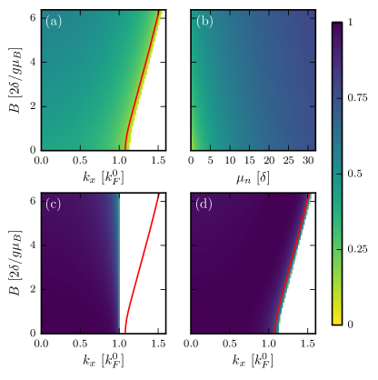
The transmission probabilities of two spin orientations follow immediately:
| (46) |
with and the velocities normal to the interface in two materials. Both and exhibit similar behavior, except for vanishing inside the helical gap. In contrast, is always well defined at for . For concreteness, we illustrate the dependence of on the Hamiltonian parameters.
Let us first start with realistic parameters both in the superconductor and the semiconductor. The chemical potential in the nanowire is gate tunable. We choose to fix it at , comparable to the level spacing in a nanowire. The rest of the parameters are specified in Sec. IV.2. The results are plotted in Fig. 12(a), for all momenta in the semiconductor Fermi surface and an experimentally relevant range of magnetic fields. The transparency is mostly around but rapidly vanishes near the Fermi momentum. Modifying the chemical potential in the wire does not appreciably increase the transparency [see Fig. 12(b)]. The low transparency is artificial and due to the choice of a sharp change in mass and chemical potential across the interface.
Choosing and results in a nearly perfect transmission at all angles, as shown in Fig. 12(c). However, this parameter choice is also unphysical since the semiconductor Fermi surface becomes larger than the superconductor one at any finite magnetic field. Then the interface becomes opaque for higher momenta .
Finally, choosing and an anisotropic mass in the superconductor , with results in an interface that stays transparent for all [see Fig. 12(d)].
Appendix B Independence of critical magnetic field on the superconducting gap
Here we verify the validity of our conclusions about the scaling of the eigenenergies and the independence of on using exact diagonalization of a finite BdG Hamiltonian for the semiconductor-superconductor heterostructure at different values of the superconducting gap. We use the same setup of a finite heterojunction modeled with the BdG Hamiltonian (18) as in Sec. VI. We check the behavior of the critical field and the bulk band gap by tracking the energy of the second excited state while varying for values of ranging from to (almost two orders of magnitude). Our results for a heterojunction of size with a normal region occupying are shown in Fig. 13.
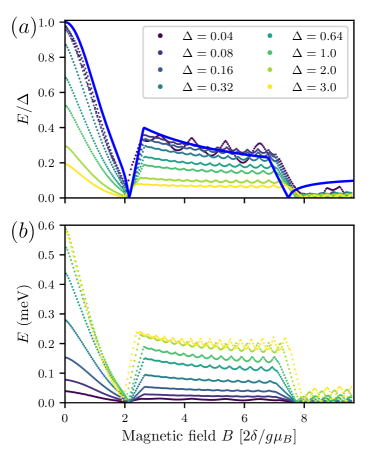
When the system transitions to the long junction regime, so that the ratio continues to decrease, while becomes almost independent on . In the opposite limit , we observe that tends to a constant, in agreement with the short-junction limit prediction. The field values where vanishes stay almost constant, with the residual variation due to the effect of a finite system size and lattice constant.
References
- Qi and Zhang (2011) X.-L. Qi and S.-C. Zhang, Rev. Mod. Phys. 83, 1057 (2011).
- Leijnse and Flensberg (2012) M. Leijnse and K. Flensberg, Semicond. Sci. Technol. 27, 124003 (2012).
- Alicea (2012) J. Alicea, Rep. Prog. Phys. 75, 076501 (2012).
- Beenakker (2013) C. Beenakker, Annu. Rev. Condens. Matter Phys. 4, 113 (2013).
- Elliott and Franz (2015) S. R. Elliott and M. Franz, Rev. Mod. Phys. 87, 137 (2015).
- Lutchyn et al. (2010) R. M. Lutchyn, J. D. Sau, and S. Das Sarma, Phys. Rev. Lett. 105, 077001 (2010).
- Oreg et al. (2010) Y. Oreg, G. Refael, and F. von Oppen, Phys. Rev. Lett. 105, 177002 (2010).
- Chang et al. (2015) W. Chang, S. M. Albrecht, T. S. Jespersen, F. Kuemmeth, P. Krogstrup, J. Nygard, and C. M. Marcus, Nat. Nanotechnol. 10, 232 (2015).
- Deng et al. (2016) M. T. Deng, S. Vaitiekėnas, E. B. Hansen, J. Danon, M. Leijnse, K. Flensberg, J. Nygård, P. Krogstrup, and C. M. Marcus, Science 354, 1557 (2016).
- Albrecht et al. (2016) S. M. Albrecht, A. P. Higginbotham, M. Madsen, F. Kuemmeth, T. S. Jespersen, J. Nygård, P. Krogstrup, and C. M. Marcus, Nature 531, 206 (2016).
- Cole et al. (2015) W. S. Cole, S. Das Sarma, and T. D. Stanescu, Phys. Rev. B 92, 174511 (2015).
- Clogston (1962) A. M. Clogston, Phys. Rev. Lett. 9, 266 (1962).
- Beenakker (2005) C. W. J. Beenakker, in Quantum Dots: a Doorway to Nanoscale Physics, Lecture Notes in Physics No. 667, edited by W. D. Heiss (Springer Berlin Heidelberg, 2005) pp. 131–174.
- Bezuglyi et al. (2002) E. V. Bezuglyi, A. S. Rozhavsky, I. D. Vagner, and P. Wyder, Phys. Rev. B 66, 052508 (2002).
- Dimitrova and Feigel’man (2006) O. V. Dimitrova and M. V. Feigel’man, J. Exp. Theor. Phys. 102, 652 (2006).
- Cheng and Lutchyn (2012) M. Cheng and R. M. Lutchyn, Phys. Rev. B 86, 134522 (2012).
- Liu et al. (2012) J. Liu, A. C. Potter, K. T. Law, and P. A. Lee, Phys. Rev. Lett. 109, 267002 (2012).
- Stanescu et al. (2013) T. D. Stanescu, R. M. Lutchyn, and S. Das Sarma, Phys. Rev. B 87, 094518 (2013).
- Peng et al. (2015) Y. Peng, F. Pientka, L. I. Glazman, and F. von Oppen, Phys. Rev. Lett. 114, 106801 (2015).
- Pöyhönen et al. (2016) K. Pöyhönen, A. Westström, and T. Ojanen, Phys. Rev. B 93, 014517 (2016).
- Wimmer et al. (2010) M. Wimmer, A. R. Akhmerov, M. V. Medvedyeva, J. Tworzydło, and C. W. J. Beenakker, Phys. Rev. Lett. 105, 046803 (2010).
- Lutchyn et al. (2011) R. M. Lutchyn, T. D. Stanescu, and S. Das Sarma, Phys. Rev. Lett. 106, 127001 (2011).
- Cole et al. (2016) W. S. Cole, J. D. Sau, and S. Das Sarma, Phys. Rev. B 94, 140505 (2016).
- van Heck et al. (2014) B. van Heck, S. Mi, and A. R. Akhmerov, Phys. Rev. B 90, 155450 (2014).
- Andreev (1964) A. F. Andreev, Zh. Eksp. Teor. Fiz. 46, 1823 (1964), [Sov. Phys. JETP 19, 1228 (1964)].
- Bardarson (2008) J. H. Bardarson, J. Phys. A-Math. Theor. 41, 405203 (2008).
- Beenakker (2015) C. W. J. Beenakker, Rev. Mod. Phys. 87, 1037 (2015).
- Beenakker (1991) C. W. J. Beenakker, Phys. Rev. Lett. 67, 3836 (1991).
- BenDaniel and Duke (1966) D. J. BenDaniel and C. B. Duke, Phys. Rev. 152, 683 (1966).
- Mourik et al. (2012) V. Mourik, K. Zuo, S. M. Frolov, S. R. Plissard, E. P. a. M. Bakkers, and L. P. Kouwenhoven, Science 336, 1003 (2012).
- Groth et al. (2014) C. W. Groth, M. Wimmer, A. R. Akhmerov, and X. Waintal, New J. Phys. 16, 063065 (2014).
- Nijholt and Akhmerov (2016) B. Nijholt and A. R. Akhmerov, Phys. Rev. B 93, 235434 (2016).
- Klinovaja and Loss (2012) J. Klinovaja and D. Loss, Phys. Rev. B 86, 085408 (2012).
- Schnyder et al. (2009) A. P. Schnyder, S. Ryu, A. Furusaki, and A. W. W. Ludwig, AIP Conf. Proc. 1134, 10 (2009).
- Ryu et al. (2010) S. Ryu, A. P. Schnyder, A. Furusaki, and A. W. W. Ludwig, New J. Phys. 12, 065010 (2010).
- Tewari and Sau (2012) S. Tewari and J. D. Sau, Phys. Rev. Lett. 109, 150408 (2012).
- Lim et al. (2013) J. S. Lim, R. López, and L. Serra, EPL (Europhysics Letters) 103, 37004 (2013).
- Osca et al. (2014) J. Osca, R. López, and L. Serra, Eur. Phys. J. B 87, 84 (2014).
- Osca and Serra (2015) J. Osca and L. Serra, Phys. Rev. B 91, 235417 (2015).
- Note (1) The code for the tight-binding simulations of the two-dimensional and three-dimensional junctions is available in ancillary files to the manuscript.