Resistivity of the insulating phase approaching the 2D metal-insulator transition: the effect of spin polarization
Abstract
The resistivities of the dilute, strongly-interacting 2D electron systems in the insulating phase of a silicon MOSFET are the same for unpolarized electrons in the absence of magnetic field and for electrons that are fully spin polarized by the presence of an in-plane magnetic field. In both cases the resistivity obeys Efros-Shklovskii variable range hopping , with and mapping onto each other if one applies a shift of the critical density reported earlier. With and withoug magnetic field, the parameters and exhibit scaling consistent with critical behavior approaching a metal-insulator transition.
pacs:
71.30.+h, 72.20.Ee, 64.60.F-Two-dimensional (2D) electron systems realized in semiconductor heterostructures and on the surface of doped semiconductor devices such as silicon MOSFETs have been intensively studied for more than half a century Ando1982 . Significant advances in fabrication techniques in recent years have yielded samples with greatly increased electron mobility thereby allowing access to lower electron densities, a regime where the energy of interactions between the electrons is dominant and substantially larger than their kinetic energy. Rather than exhibiting a resistivity that increases logarithmically toward infinity as the temperature is reduced DolanDynes as expected within the theory of localization Abrahams1979 , the resistivity of these strongly-interacting dilute 2D electron systems displays metallic-like behavior at low temperatures and insulating behavior as the electron density is reduced below a material-dependent critical electron density (see references Abrahams2001 ; KravchenkoReports ; Spivak2009 for reviews). The apparent metal-insulator transition and metallic phase observed in high-mobility, strongly interacting 2D electron systems is widely regarded as one of the most important unresolved problems in condensed matter physics.
Exceptionally large magnetoresistances have been reported in response to in-plane magnetic field in the vicinity of the critical electron density, . For electron densities on the just-metallic side of the transition, increasing the parallel magnetic field causes the resistivity to increase by several orders of magnitude at low temperatures and reach saturation at a density-dependent field ; for the temperature dependence of the resistivity is that of an insulator. Measurements have confirmed that the saturation of the sample resistivity corresponds to full spin polarization Okamoto1999 ; Vitkalov2000 . Since the parallel magnetic field does not couple to the orbital motion of electrons in sufficiently thin 2D systems, this suggests an important role for the electron spins.
The magnetoresistance has been thoroughly investigated on the metallic side of the transition, while considerably less information has been gathered in the insulating phase. In order to better understand the effect of spin, we embarked on a detailed comparison of the resistivity of the insulating state arrived at by: (1) reducing the electron density below the critical density in zero field so that the electrons are unpolarized, or (2) applying an in-plane magnetic field beyond the saturation field where the metallic behavior is suppressed and the spins are fully polarized.
It has been established in a number of experiments that the application of in-plane magnetic field causes a shift of the critical density Simonian1997 ; Pudalov1997 ; Mertes1999 ; Jaroszynski2004 ; Shashkin2001 . As further detailed below, there have been conflicting reports on the behavior of the resistivity in the insulating phase of low-disorder 2D materials, with some claiming simply-activated behavior and others claiming Efros-Shklovskii variable-range hopping in the presence of a Coulomb gap due to electron interactions Shklovskii1984 .
In this paper we report that both in zero field and in the presence of an in-plane magnetic field sufficient to polarize all the carriers, the resistivity obeys Efros-Shklovskii variable-range hopping. Moreover, we demonstrate that the unpolarized insulator and the fully spin-polarized insulator map onto each other if one simply shifts the critical density . This implies that the transport properties of the insulating state are the same in an unpolarized and in a completely spin-polarized system.
Measurements were performed on silicon metal-oxide-semiconductor field-effect transistors (MOSFETs) between 0.25 K and 2 K in an Oxford Heliox He-3 refrigerator in the absence of magnetic field and in a parallel field of 5 T. Similar to those used in Ref. Mokashi2012 , the high-mobility samples used in our studies ( cm2/Vs) were fabricated in a Hall bar geometry of width 50 m and distance 120 m between the central potential probes; the oxide thickness was 150 nm. Contact resistance was minimized by using a split-gate geometry in which thin gaps are introduced in the gate metallization so that a high electron density can be maintained near the contacts independently of the value of the electron density in the main part of the sample. Electron densities were controlled by applying a positive dc gate voltage relative to the contacts.
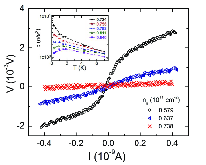
As shown in Fig. 1, the voltage is a strongly nonlinear function of the current: it exhibits linear (ohmic) behavior at low currents and bends to a lower slope above a current that depends on electron density and temperature. This is in agreement with numerous past measurements and has variously been attributed to non-ohmic strong electric field Efros-Shklovskii variable range hopping Marianer1992 , or the depinning of a Wigner Crystal or charge-density wave Goldman1990 ; Kravchenko1991 ; D'Iorio1992 ; Pudalov1993 ; Pudalov1994 . The resistivity plotted in the next few figures was deduced from the low-current, linear portion of the curves measured for each and Mason1995 .
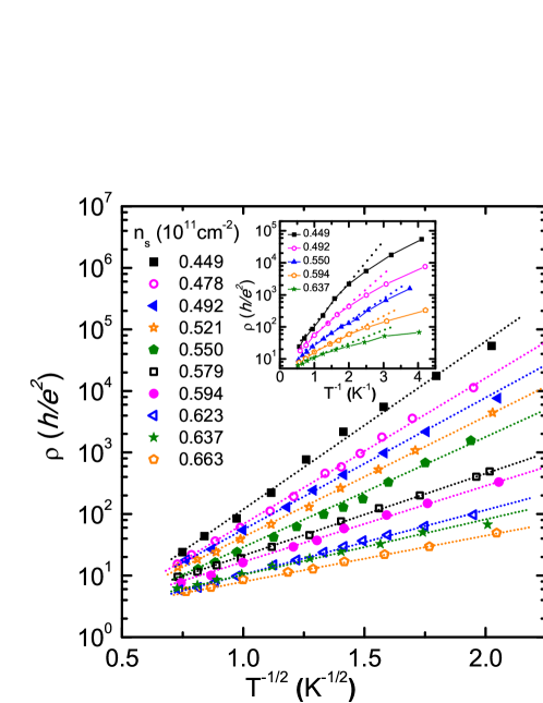
Figure 2 shows the log of the resistivity measured in zero field plotted against for electron densities . For comparison, the inset shows the same data plotted as a function of . Quite clearly, the data obey the Efros-Shklovskii form of variable-range hopping in the temperature range of the measurements (0.25 K to 2 K). Small deviations at the lowest temperature may be due to poor thermal contact of the electron system to the lattice (and thermometer).
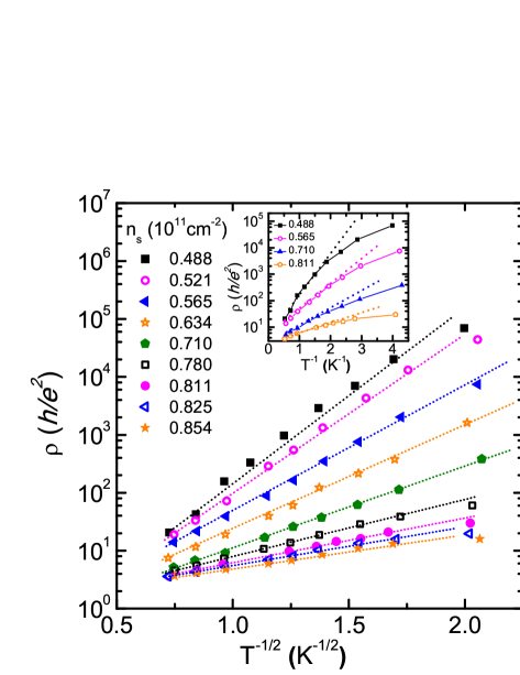
Similar data obtained in a parallel field T are shown on a semilog plot in Fig. 3, as a function of in the main figure and as a function of in the inset. Care was taken to check that T is beyond the saturation fields at the densities we used for the measurement, so that all the spins in the sample are fully polarized. The Efros-Shklovskii form of variable-range hopping, exp provides an excellent fit to the data in parallel magnetic field.
In a doped semiconductor at relatively low temperature where there is not enough (thermal) energy to activate electrons across the mobility edge to conducting states in the impurity band, charge transport occurs via thermally activated hopping between localized states, obeying the expression
| (1) |
Here the exponent = 1 for nearest-neighbor hopping, for Mott variable-range hopping in two dimensions Mott1969 , and for Efros-Shklovskii variable-range hopping in the presence of a Coulomb gap in the density of states associated with electron-electron interactions Efros1975 ; Shklovskii1984 .
There have been a number of studies of the resistivity of silicon MOSFETs in the insulating phase. The temperature dependence of the resistivity in zero field was attributed to Efros-Shklovskii variable range hopping with down to K by Mertes Mertes1999 and Jarozynski Jaroszynski2004 and over a broader range to lower temperatures by Mason Mason1995 . The zero-field resistivity was found to obey the same form in a single two-dimensional layer of -doped GaAs/AlxGa1-xAs Shlimak2000 . By contrast, Arrhenius-type activated behavior () was claimed for silicon in zero field by Shashkin Shashkin2001 .
Measurements in the presence of an in-plane magnetic field have yielded various different results: Shashkin fitted data for silicon at intermediate temperatures and densities near the transition to the activated form with Shashkin2001 ; also in silicon, Mertes applied a high parallel magnetic field T and found a larger exponent Mertes2001 . For a single two-dimensional layer of -doped GaAs/AlxGa(1-x)As in parallel fields of 8 T and 6 T, Shlimak reported an exponent of 0.8 Shlimak2000 .
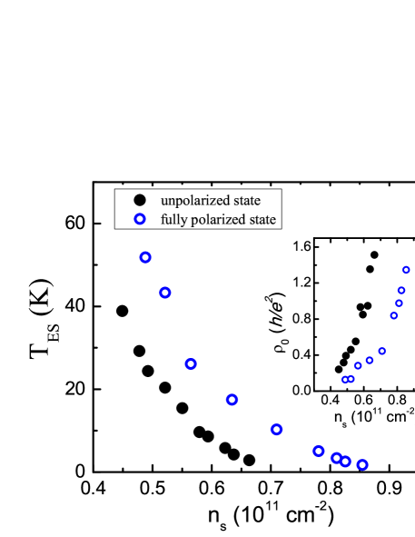
As shown in Fig. 2 and Fig. 3 above, the data reported here in zero field and in 5 T parallel field are both consistent with Efros-Shklovskii variable-range hopping, exp footnote . The parameters in zero field and (5T) in 5 T parallel field are shown in Fig. 4 as a function of electron density. and (5T) both decrease and gradually approach zero. While extrapolates to zero at critical density in the absence of magnetic field, (5T) obtained in a 5 T parallel field extrapolates to zero at a different electron density which we designate as (5T) = . The inset to Fig. 4 shows that the prefactor increases sharply with increasing electron density.
The critical density in zero field is generally determined as the density at which the temperature derivative of the resistivity, , changes sign; an example of such a ”separatrix” between metallic and insulating behavior can be seen in the inset to Fig. 1. The authors of Ref. Shashkin2001 have shown that in zero field the density where the nonlinearity of current-voltage (I-V) characteristics vanishes yields the same critical density. Using both protocols, the critical density in zero field was estimated to be cm-2 for our sample. We note that this is the critical density inferred from thermoelectric power measurements on the same sample Mokashi2012 .
An estimate of the critical density in a T field can be obtained by determining the density at which the nonlinearity in the I-V characteristic vanishes Shashkin2001 . Using this procedure, an estimate is obtained for the critical electron density at in our sample of cm-2.
In Efros and Shklovskii’s theory of variable-range hopping conduction for strongly interacting electrons, the parameter , where and are the density-dependent dielectric constant and localization length, respectively Shklovskii1984 . Moreover, and as electron density approaches the critical density from the insulating side, so that obeys the critical form:
| (2) |
where .
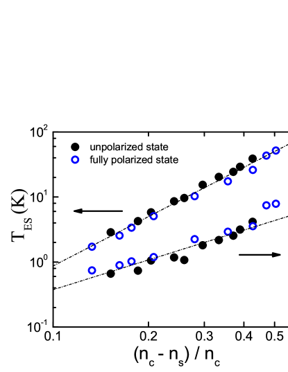
Using the values estimated for and , we now plot in zero field (filled circles) and in 5 T parallel field (triangles) as a function of and , respectively, on a log-log scale in Fig. 5. in the unpolarized state and in the fully polarized state at 5 T lie on the same curve. Relative to the appropriate critical density for each case, the Efros-Shklovskii parameter approaches the metallic phase with the same critical exponent, with . Interestingly, the prefactor is also consistent with critical behavior.
Although our data and many past experiments are consistent with the occurrence of a transition, it is noteworthy and puzzling that the value we’ve obtained for the critical exponent is substantially different from the smaller exponents in the vicinity of reported in a number of earlier studies exp1.6 . Our analysis is based on data obtained quite far from the transition and entails two parameters, and , while earlier analyses using a single parameter were based on data obtained near and on both sides of the presumed critical point. A careful examination shows that the portion of our data that is near the transition is consistent with one-parameter scaling and a smaller exponent of , while the portion of the published data that is further from the transition is can be scaled using two parameters, and with much closer to our value of footnote2 . Thus, there is no discrepancy between data sets, and the difference may be due to relative closeness to the critical regime.
As suggested in Ref. Mokashi2012 , there may indeed be two quantum critical points in play: driven by disorder, and a disorder-independent universal interaction-driven critical point . They are different in principle, but so close to each other in the low-disorder samples of our studies that they have not been separately identified experimentally. The scaling of and is determined using data obtained in the insulating phase only, and it is by no means clear which (if either) critical point it refers to. This raises the possibility that there may be two closely spaced transitions, one driven by disorder and one driven by interactions. In the range of densities just below the transition where the temperature derivative of the resistivity, , is negative indicating insulating behavior, the resistivity is a very weak function of temperature so that it cannot be reliably fit to the Efros-Shklovskii form. It is thus possible that there is an intermediate phase in this region that gives rise to different exponents entering and leaving this phase as the density is increased. Additional careful studies to lower temperatures of samples with yet lower disorder in this range of densities would be of great interest.
To summarize, we have measured the resistivity of the dilute, strongly-interacting 2D electron system in a silicon MOSFET in the insulating phase arrived at by (1) reducing the electron density in the absence of magnetic field, which results in no spin polarization (2) applying a 5 Tesla in-plane field which results in complete spin polarization. For both cases, the resistivity obeys Efros-Shklovskii variable-range hopping with parameters and that are consistent with critical behavior approaching a metal-insulator transition. The sole effect of spin polarization is a simple shift of the critical density. The fact that the transport properties of the insulating state are the same in two systems with different spin configurations should be very interesting and worth further theoretical attention.
Useful comments were provided by Steve Kivelson, Boris Spivak, Vladimir Dobrosavljevic and Dragana Popovic. We thank Boris Shklovskii, Dietrich Belitz and Sergey Kravchenko for numerious discussions, valuable insights and for their critical reading of this manuscript. This work was supported by the National Science Foundation grant DMR-1309008 and the Binational Science Foundation Grant 2012210.
References
- (1) For example, see T. Ando, A. B. Fowler and F. Stern, Rev. Mod. Phys. 54, 437 (1982).
- (2) G. J. Dolan and D. D. Osheroff, Phys. Rev. Lett. 43, 721 (1979); D. J. Bishop, D. C. Tsui, and R. C. Dynes, Phys. Rev. Lett. 44, 1153 (1980); M. J. Uren, R. A. Davies, and M. Pepper, J. Phys. C 13, L985 (1980).
- (3) E. Abrahams, P. W. Anderson, D. C. Licciardello, and T. V. Ramakrishnan, Phys. Rev. Lett. 42, 673 (1979).
- (4) E. Abrahams, S. V. Kravchenko, and M. P. Sarachik, Rev. Mod. Phys. 73, 251 (2001).
- (5) S. V. Kravchenko and M. P. Sarachik, Rep. Prog. Phys. 67, 1 (2004).
- (6) B. Spivak, S. V. Kravchenko S. A. Kivelson, and X. P. A. Gao, Rev. Mod. Phys. 82, 1743 (2009).
- (7) Tohru Okamoto, Kunio Hosoya, Shinji Kawaji, and Atsuo Yagi, Phys. Rev. Lett. 82, 3875 (1999).
- (8) S. A. Vitkalov, Hairong Zheng, K. M. Mertes, M. P. Sarachik, and T. M. Klapwijk, Phys. Rev. Lett. 85, 2164 (2000); S. A. Vitkalov, M. P. Sarachik and T. M. Klapwijk, Phys. Rev. B 64, 073101 (2001).
- (9) D. Simonian, S. V. Kravchenko, M. P. Sarachik, and V. M. Pudalov, Phys. Rev. Lett. 79, 2304 (1997)
- (10) V. M. Pudalov, G. Brunthaler, A. Prinz, and G. Bauer, JETP Lett. 65, 932 (1997).
- (11) K. M. Mertes, D. Simonian, M. P. Sarachik, S. V. Kravchenko, and T. M. Klapwijk, Phys. Rev. B 60, R5093 (1999).
- (12) A. A. Shashkin, S. V. Kravchenko, and T. M. Klapwijk, Phys. Rev. Lett. 87, 266402 (2001).
- (13) J. Jaroszynski, Dragana Popovic, and T. M. Klapwijk, Phys. Rev. Lett. 92, 226403 (2004).
- (14) B. I. Shklovskii, A. L. Efros, Electronic Properties of Doped Semiconductors, Solid State Series Vol. 45 (Springer-Verlag Berlin Heidelberg, 1984).
- (15) A. Mokashi, S. Li, Bo Wen, S. V. Kravchenko, A. A. Shashkin, V. T. Dolgopolov, M. P. Sarachik, Phys. Rev. Lett. 109, 096405 (2012).
- (16) S. Marianer and B. I. Shklovskii, Phys. Rev. B 46, 13100 (1992).
- (17) V. J. Goldman, M. Santos, M. Shayegan, and J. E. Cunningham, Phys. Rev. Lett. 65, 2189 (1990).
- (18) S. V. Kravchenko, V. M. Pudalov, J. Campbell, and M. D’Iorio, JETP Lett.54, 532 (1991).
- (19) M. D’Iorio, V. M. Pudalov, and S. G. Semenchinsky, Phys. Rev. B 46, 15992 (1992).
- (20) V. M. Pudalov, M. D’Iorio, S. V. Kravchenko, and J. W. Campbell, Phys. Rev. Lett. 70, 1866 (1993).
- (21) V. M. Pudalov and S. T. Chui, Phys. Rev. B 49, 14062 (1994).
- (22) W. Mason, S. V. Kravchenko, G. E. Bowker, and J. E. Furneaux, Phys. Rev. B 52, 7857 (1995).
- (23) N. F. Mott, Philosophical Magazine, 19, 835 (1969).
- (24) A. L. Efros and B. I. Shklovskii, J. Phys. C, L49, 8 (1975).
- (25) I. Shlimak, S. I. Khondaker, M. Pepper, and D. A. Ritchie, Phys. Rev. B 61, 07253 (2000).
- (26) K. M. Mertes, Hairong Zheng, S. A. Vitkalov, M. P. Sarachik, and T. M. Klapwijk, Phys. Rev. B 63, 041101(R) (2001).
- (27) Acceptable fits to our data can be obtained to the expression using a temperature-dependent prefactor. This yields a strongly negative value of for , a small positive value of x consistent with for and for . Although little is known about the range of acceptable values for , these numbers suggest that and (a temperature-independent prefactor) is a reasonable choice. Data over a broader range of temperature could restrict the range for acceptable fits.
- (28) S. V. Kravchenko, Whitney E. Mason, G. E. Bowker, J. E. Furneaux, V. M. Pudalov, and M. D’Iorio, Phys. Rev. B 51, 7038 (995); S. V. Kravchenko, D. Simonian, M. P. Sarachik, Whitney Mason, and J. E. Furneaux, Phys. Rev. Lett. 77, 4938 (1996); Dragana Popovic, A. B. Fowler, and S. Washburn, Phys. Rev. Lett. 79, 1543 (1997); X. G. Feng, Dragana Popovic, and S. Washburn, Phys. Rev. Lett. 83, 368 (1999).
- (29) The value is very close to the critical exponent expected for a classical percolation transition. However, the disorder potential in Si is short-range so the possibility of a percolation transition can be safely ruled out.