Modeling the Excitation of Graphene Plasmons in Periodic Grids of Graphene Ribbons: An Analytical Approach
Abstract
We study electromagnetic scattering and subsequent plasmonic excitations in periodic grids of graphene ribbons. To address this problem, we develop an analytical method to describe the plasmon-assisted absorption of electromagnetic radiation by a periodic structure of graphene ribbons forming a diffraction grating for THz and mid-IR light. The major advantage of this method lies in its ability to accurately describe the excitation of graphene surface plasmons (GSPs) in one-dimensional (1D) graphene gratings without the use of both time-consuming, and computationally-demanding full-wave numerical simulations. We thus provide analytical expressions for the reflectance, transmittance and plasmon-enhanced absorbance spectra, which can be readily evaluated in any personal laptop with little-to-none programming. We also introduce a semi-analytical method to benchmark our previous results and further compare the theoretical data with spectra taken from experiments, to which we observe a very good agreement. These theoretical tools may therefore be applied to design new experiments and cutting-edge nanophotonic devices based on graphene plasmonics.
I Introduction
Nowadays, photonics — dubbed “the science of light” — is one of the branches of the physical sciences with most impact in our daily lives. It is concerned with the study and manipulation of light (photons) in a manifold of fundamental and technological landscapes. Recently, the “nano-revolution” under way has led to the miniaturization of electronics. However, in what regards electromagnetic (EM) radiation, such miniaturization is limited by the length-scale defined by the wavelength of the employed light (known as the diffraction-limit). In this context, plasmonicsMaradudin et al. (2014) has been regarded as the most promising candidate to bring EM fields to the nanoscale.Barnes et al. (2003); Gramotnev and Bozhevolnyi (2010); Schuller et al. (2010); Armstrong (2012); Ozbay (2006) Plasmonics is a branch of photonics which deals with quasiparticles known as plasmon-polaritons.Maradudin et al. (2014); Toropov and Shubina (2015) Surface plasmon-polaritons (SPPs) are electromagnetic surface waves coupled to collective excitations of the free electrons in conductors. When these hybrid excitations occur in conducting nanostructures — such as nanoparticlesPelton et al. (2008); Pelton and Bryant (2013) or engineered metamaterialsBillings (2013); Zheludev and Kivshar (2012) —, the corresponding non-propagating plasmon-polaritons are generally coined as localized surface plasmons (LSPs).Maradudin et al. (2014) Perhaps the most alluring property of plasmons is that they exhibit large field-enhancements and deep subwavelength confinement of EM fields, thereby circumventing the diffraction limit of conventional optics.Barnes et al. (2003); Gramotnev and Bozhevolnyi (2010); Schuller et al. (2010); Armstrong (2012) For this reason, plasmonics has been considered the ultimate pathway to manipulate light-matter interactions at the nanometer scale.
Very recently, grapheneGeim (2009); Neto et al. (2009); Ferrari et al. (2015) — a two-dimensional (2D) crystal made up of carbon atoms arranged in a honeycomb lattice — has emerged as a promising plasmonic material, benefiting from this material’s remarkable electronic and optical properties.Neto et al. (2009); Ferrari et al. (2015); Avouris (2010); Bonaccorso et al. (2010) Doped graphene is capable of supporting SPPs — graphene surface plasmon-polaritons (GSPs)Grigorenko et al. (2012); de Abajo (2014); Xiao et al. (2016); Low and Avouris (2014); Koppens et al. (2011); Bludov et al. (2013); Politano and Chiarello (2014); Gonçalves and Peres (2016) — in the THz and mid-IR spectral range. These possess tantalizing properties, outperforming traditional noble-metal plasmonics, in that spectral window, in terms of mode confinement, and are predicted to suffer from relatively low losses when compared to customary three-dimensional (3D) metals.Koppens et al. (2011); de Abajo (2014); Xiao et al. (2016); Khurgin and Boltasseva (2012) In addition, graphene plasmons have yet another key advantage: the ability of being actively tunable by means of electrical gating or chemical doping. This feature constitutes a major improvement over conventional metal-based plasmonicsMaradudin et al. (2014); Toropov and Shubina (2015) (where tunability is usually limited by the geometry and composition of the system, and therefore it is fixed), and constitutes a sought-after characteristic for active nanophotonic devices and/or circuitry based on graphene plasmons. Indeed, a plethora of proof-of-concept, application-oriented experiments have already demonstrated the capabilities of GSPs to deliver extremely sensitive biochemical sensors,Rodrigo et al. (2015); Farmer et al. (2016); Wang et al. (2013); Zeng et al. (2015); Zhao et al. (2013) surface-enhanced Raman scattering (SERS),Ling et al. (2010); Xu et al. (2012); Zhao et al. (2014); Liu et al. (2011a); Heeg et al. (2013); Urich et al. (2012) polarizers,Bao et al. (2011); Sorger et al. (2015) optical modulatorsSun et al. (2016a); Sensale-Rodriguez et al. (2012); Yu et al. (2015); Sensale-Rodriguez et al. (2013) and photodetectors.Fang et al. (2012a); Liu et al. (2011b); Sun et al. (2016b); Echtermeyer et al. (2016); Koppens et al. (2014)
Such achievements are particularly notable in the light that optical excitation of graphene plasmons was only achieved as recently as in 2011 by Ju et al., using periodic arrays of graphene microribbons.Ju et al. (2011) That foundational publication paved the way for the emergence of many experimental and theoretical works that soon followed, thereby establishing the field of graphene plasmonics.Gonçalves and Peres (2016); Grigorenko et al. (2012); de Abajo (2014); Xiao et al. (2016); Koppens et al. (2011); Low and Avouris (2014); Bludov et al. (2013); Politano and Chiarello (2014) As of today, GSPs have been realized in a number of systems, ranging from patterned grids of graphene ribbons,Ju et al. (2011); Yan et al. (2013); Nene et al. (2014); Rodrigo et al. (2015); Farmer et al. (2016); Sorger et al. (2015); Sensale-Rodriguez et al. (2012); Yan et al. (2012a); Luxmoore et al. (2014); Hu et al. (2015) disks,Yan et al. (2012b, a); Fang et al. (2013, 2014); Zhu et al. (2014) and rings, Fang et al. (2013); Yan et al. (2012b) periodic anti-dot lattices,Liu et al. (2015); Zhu et al. (2014); Yeung et al. (2014) resonators,Brar et al. (2013, 2014) hybrid graphene/metal nano-antennas,Yao et al. (2013); Fang et al. (2012a, b); Liu et al. (2011b); Alonso-González et al. (2014) among others.Gao et al. (2013); Zhu et al. (2013); Fei et al. (2011); Yan et al. (2012c); Constant et al. (2015); Tokman et al. (2016); Fei et al. (2012); Chen et al. (2012); Woessner et al. (2015); Barcelos et al. (2015)
In the heart of plasmonics lies the fact that freely-propagating EM radiation cannot couple directly to plasmons owing to the momentum mismatch between plasmons and photons of the same frequency. However, the property that the plasmon’s wavevector is larger than the wavevector of light of the same frequency is exactly what enables extreme localization of light into subwavelength volumes. For extended graphene, these volumes can be about times smaller (where denotes the fine-structure constant) than the volume characterized by the free-space light’s wavelength (i.e. ). Typical strategies to couple light to graphene plasmons involve the patterning of pristine graphene into gratings and related nanostructures,Ju et al. (2011); Yan et al. (2013); Nene et al. (2014); Rodrigo et al. (2015); Sorger et al. (2015); Sensale-Rodriguez et al. (2012); Yan et al. (2012a); Luxmoore et al. (2014); Hu et al. (2015); Farmer et al. (2016); Yan et al. (2012b, a); Fang et al. (2013, 2014); Zhu et al. (2014); Liu et al. (2015); Zhu et al. (2014); Yeung et al. (2014) the use of dielectric gratings,Gao et al. (2013); Zhu et al. (2013) light scattering from a conductive tip,Fei et al. (2012); Chen et al. (2012); Woessner et al. (2015); Barcelos et al. (2015) and even non-linear three-wave mixing.Constant et al. (2015); Tokman et al. (2016)
In this context, the utilization of periodic grids of graphene ribbons — fabricated by patterning an otherwise continuous graphene sheet — has been one of the most popular setups to realize graphene plasmons with energies from the THz up to the mid-IR regime, which can be tailored either by varying the size of the ribbons or by tuning the concentration of charge-carriers in graphene (and thus the Fermi level). Under this scheme, the array of graphene ribbons effectively acts as a diffraction grating for EM radiation impinging on the system (e.g. from a laser), producing scattered waves which carry momenta in multiples of the reciprocal lattice vector, (where is the grating period), thus overcoming the above-mentioned kinematic constraint. The reason the use of ribbon arrays to couple light to GSPs has been so predominant is essentially two-fold (apart from being easily attainable with current fabrication technologies): it enable us to overcome the momentum mismatch between light and GSPs; and it renders a stronger (composite) plasmonic response than one would get from a single graphene ribbon (also, in this latter case, instead of well-defined diffracted orders, the scattered waves would transport a continuum of momenta).
In this work we develop an analytical framework describing the interaction of EM radiation with periodic grids of micro- and nano-sized graphene ribbons. The main motivation driving this work was to deliver a simple and transparent theoretical tool capable of explaining the plasmon-induced spectra measured in experiments that did not involve the use of computationally-heavy and time-consuming numerical simulations. Here, we provide simple closed-form expressions for the reflectance, transmittance and absorbance spectra of THz and mid-IR light through graphene patterned into ribbons. These spectra may then be used to design or model experiments with graphene plasmons in the laboratory, by simply evaluating an analytical expression. The coupling between graphene plasmons and surface optical (SO) phonon modes of a SiO2 substrate is also considered, and we observe a reconstruction of the polaritonic spectrum owing to the hybridization of GSPs with SO phonons of the underlying polar substrate. We further introduce a semi-analytical technique developed elsewherePeres et al. (2012); Bludov et al. (2012); Slipchenko et al. (2013); Bludov et al. (2013); Gonçalves and Peres (2016) to benchmark our analytical theory. Finally, we compare the outcomes of both frameworks against actual experimental data and demonstrate their ability to describe plasmonic excitations in periodic gratings of graphene ribbons.
II Theory
II.1 Analytical Method
We consider the scattering of EM radiation by a 1D periodic grid of graphene ribbons of width . For the sake of simplicity, the ribbons are assumed to possess infinite length in the longitudinal direction. In such an arrangement, the graphene grid behaves like a diffraction grating for EM waves. The period of the grating is denoted by hereafter, and the system is assumed to lie in the plane defined by , being cladded between two dielectric media with relative permittivities (for ) and (for ) — see Fig. 1. In what follows, we assume ribbons whose widths are nm or larger, so that the actual edge termination of the graphene ribbons and finite-sized effects are not important, and therefore a classical electrodynamics framework suffices Thongrattanasiri et al. (2012); Christensen et al. (2014).
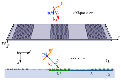
We consider a -polarized monochromatic plane-wave impinging on the grid of graphene ribbons at an angle . For such polarization, the incident EM fields read
| (1) | ||||
| (2) |
where the wavevector of the incoming wave is defined as , with and , where . Naturally, the field amplitudes , and are connected via Maxwell’s equations, which establish the relations and . Furthermore, due the periodicity of the grid, one may write the reflected magnetic field in the form of a Bloch-sum (also termed as Fourier-Floquet decomposition),
| (3) |
where an implicit time-dependence of the usual form is assumed henceforth, and where the wavevectors of the Bloch modes are defined as
| (4) |
where is the primitive vector of the reciprocal lattice. In addition, note that as determined from Maxwell’s equations. Likewise, the field transmitted across the graphene grating may also be casted as a Bloch-sum, reading
| (5) |
where . As in the case of the incident fields, we can make use of Maxwell’s curl equation to write out the corresponding reflected and transmitted electric fields from Eqs. (3) and (5). This procedure leads to
| (6) | ||||
| (7) |
respectively. At this stage, the coefficients and are still unknown. In order to determine them, one must impose the appropriate boundary conditions of the problem. To that end, we employ the first boundary condition stating that the -component of the electric field above and below the graphene grid must be continuous, , that is
| (8) |
Multiplying the previous expression with a basis function, , and integrating over the unit cell, yields
| (9) |
which links the Bloch coefficients and (and for that matter). Moreover, according to Ohm’s law, the electric fields produce a current given by , which reads
| (10) |
where is the position-dependent conductivity of graphene, which in the unit cell can be written as . In this expression, is the dynamical conductivity of a graphene ribbon (here assumed to be bulk-like) and denotes the Heaviside step function.Abramowitz and Stegun (1965)
We now introduce a central assumption into our analytic method, which is the validity of the edge condition.Barkeshli (2015) This condition states that the current perpendicular to a sharp edge — such that of a graphene ribbon — should be proportional to the square-root of the distance to the edge, , that is, . Our assumption here is that in the regime where one can interpolate the current by an expression that incorporates the edge condition at both edges of each ribbon, e.g. , simultaneously. Therefore, this ansatz allows us to write the current within a ribbon in the unit cell as
| (11) |
where is a coefficient to be determined. As a first step towards the determination of the coefficient , we now argue that Eqs. (10) and (11) must give rise to the same induced current (since they represent the same physical quantity). Hence, one may write the following relation (in the unit cell)
| (12) |
which, after multiplying by a basis function, , and integrating over the unit cell, produces
| (13) |
where is the 1st-order Bessel function of the first kind Abramowitz and Stegun (1965). This expression defines the coefficient in terms of the Bloch-amplitudes , and whose combination with Eq. (9) connects the coefficients , and . In order to close the system of equations, we require another expression relating these quantities. Such “extra” equation is the other boundary condition holding for this system, in particular, the discontinuity of the magnetic field across the graphene grid due to the presence of the surface current induced by the electric field, i.e. which, after applying the same operations that led to Eqs. (9) and (13), gives
| (14) |
thereby closing the system. Finally, the combination of Eqs. (9) and (14) allows us to write the ’s as
| (15) |
which, after using Eq. (13) endows us an expression for the coefficient (from which the Bloch amplitudes and directly follow), that is
| (16) |
where the quantity is defined as
| (17) |
It should be stressed that the sum in the previous expression needs to be judiciously performed, since it is a sum with alternating signs (check appendix A.1 for details).
II.2 Transmittance, reflectance and absorbance for normal incidence
Here we consider the particular case where the impinging radiation strikes the graphene grid at normal incidence (see appendix A.2 for oblique incidence), for which we have and , so that . In addition we remark that here, as in most experimental configurations, the -component of the scattered wavevectors remains real only for the zero-th mode, i.e. , while for the other diffraction orders it is imaginary, that is . The reason for this is that often the period of the grating is much smaller than the impinging wavelength, , and thus . This is no coincidence, since our goal is to surpass the momentum imbalance between the incident light and GSPs. This can only be effectively achieved by fabricating subwavelength gratings. Therefore, we take for henceforth. Consequently, only the zero-th mode reaches the far-field.
In possession of Eqs. (9) and (15)–(17), we have all the necessary ingredients to compute the scattering efficiencies for EM radiation striking the array of graphene ribbons. From the aforementioned expressions, the reflectance, transmittance and absorbance by the graphene grid read (see A.2 for a detailed derivation)
| (18) | ||||
| (19) | ||||
| (20) |
respectively [and recall Eqs. (16) and (17) for ]. From the inspection of the above equations it is clear that the plasmonic resonances are controlled by the poles of [or, similarly, ]. Analyzing carefully the structure of the quantity , we readily identify that these occur whenever the condition
| (21) |
weighted by the factor is met. Notice that Eq. (21) is nothing but the implicit expression for the dispersion relation of GSPs Gonçalves and Peres (2016); de Abajo (2014); Xiao et al. (2016); Low and Avouris (2014); Bludov et al. (2013) with wavevector . However, what particular Bragg modes constitute the leading contributions for GSP-excitation strongly depends on the filling ratio (please refer to appendix A.3 for further details).
III Results and Discussion
III.1 Signatures of graphene plasmon resonances
Having formulated our analytical model, we are now able to compute the absorbance, reflectance and transmittance spectra of EM radiation impinging on a periodic grid of graphene ribbons at normal incidence. Therefore, the results presented below are based on the outcome of Eqs. (18)–(20). In the following, we take the conductivity of the graphene ribbons as the Drude conductivity of bulk-graphene (see appendix B). This is a rather good approximation for doped graphene ribbons in the THz spectral range, as long as the ribbons are not too small (e.g. wider than several tens of nanometers Thongrattanasiri et al. (2012); Christensen et al. (2014)). In particular, in Fig. 2 we show the absorbance spectra (left panel) and corresponding reflectance and transmittance spectra (right panel) for different values of the damping parameter, .
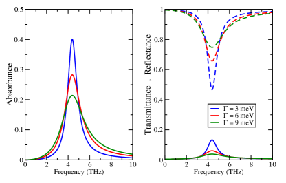
The main feature figuring in the various spectra is the presence of a well-defined peak in absorption signalling the excitation of graphene plasmons. This GSP-assisted effect yields a dramatic enhancement in the absorbance spectra of the grating, owing to the coupling of free-propagating THz radiation to plasmons supported by the graphene ribbons which compose the periodic grid. Note that the aforementioned GSP-induced absoption comes hand in hand with a supression in transmittance and with an increase in reflectance at the GSP resonant frequencies, which roughly correspond to the poles of (or, in other words, the zeros of ). Without surprise, smaller values of render sharper resonances, with these becoming successively broader and less pronounced as the electronic scattering rate increases. Also, the resonance frequency of the GSPs modes depends weakly on the value of , as it remains essentially unchanged despite the different values of the damping parameter.
It should be stressed that, in principle, the interaction of EM radiation with the grating gives rise to multiple plasmon resonances with (for ).Yan et al. (2013); Mikhailov and Savostianova (2005); Gonçalves and Peres (2016) The most prominent resonance corresponds to the fundamental plasmon mode, while the higher-order resonances become increasingly weaker. Note that in the present model the latter are necessarily ignored, owing to the choice of ansatz for the current [cf. Eq. (11)] which can only account for the dipole-like fundamental resonance (the one that appears in Fig. 2). Fortunately, this resonance carries most of the spectral weight (see appendix A.4) and it clearly dominates the polaritonic spectrum;Bludov et al. (2013); Gonçalves and Peres (2016) in fact, the resonances that emerge at higher frequencies are often invisible (or barely visible) in many experiments, since they can only be detected for small values of .
We now explore the dependence of the GSP-induced absorption spectra on the different parameters of the system. One of the most important parameters is the electronic density, . This quantity is related with the material’s Fermi energy via , where m/s is the Fermi velocity of the Dirac fermions in graphene.Kotov et al. (2012); Li et al. (2008) The density of graphene charge-carriers can be easily controlled by means of electrostatic gating. This possibility is of extreme relevance in graphene plasmonics, since it enables the excitation and control of tunable GSPs with tailored properties at the distance of a voltage knob. The effect of varying the electronic density within the graphene ribbons which constitute the grating is demonstrated in Fig. 3. From the figure, it is clear that GSP-resonances become stronger and shift toward higher frequencies as the density of charge-carriers increases. In order to quantify such behavior, in the right panel of Fig. 3 we have plotted the GSP-frequency (corresponding to the fundamental mode) as a function of the doping level, to which we have fitted a function of the type , having obtained for the exponent (fitting parameter)111The fitting function was obtained using the least-squares method..
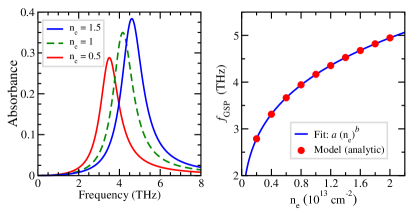
This therefore demonstrates that the observed resonances scale with the electronic density as
| (22) |
which is a specific signature of graphene plasmons.Ju et al. (2011); Yan et al. (2013); Bludov et al. (2013); Gonçalves and Peres (2016) Contrariwise, in typical 2DEGs a scaling with is observed instead. The different scaling for graphene is a direct consequence of the linear dispersion exhibited by the Dirac particles in this material. Geim (2009); Neto et al. (2009)
An alternative way to tune the GSP-resonances is to pattern grids of graphene ribbons of different widths, . For the sake of clarity, we shall keep the filling ratio constant. Figure 4 depicts the calculated absorbance spectra for periodic arrays of graphene ribbons of different widths. Notice that structures with narrower ribbons yield GSPs with higher energies. The fundamental plasmonic resonance of the grating resembles the excitation of a GSP in extended graphene with . Such large wavevectors can only be attained due to the contribution of the several Bragg diffraction orders originating from the interaction of the incident light with the grid. Within this reasoning, Fig. 4 shows that the plasmonic resonances scale as , in a similar way that plasmons in an unpatterned, continuous graphene sheet do.
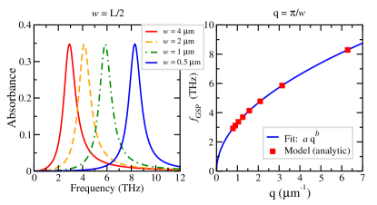
We have also found that, while the filling ratio has a significant impact on the position of the plasmonic resonance of the graphene grid, the physics of system is largely determined by the ribbon-size, i.e. provided that , that is, that the interaction between neighboring ribbons is small.
The calculated electric field akin to the graphene plasmons supported by the ribbons which constitute the grating is depicted in Fig. 5 (depicting the unit cell of a representative array of ribbons with dimensions m and m). Such computation is straightforward once the resonant frequency akin to the fundamental GSP mode is determined; that information is then fed into the Bloch amplitudes (9) and (15) that represent the scattered field.
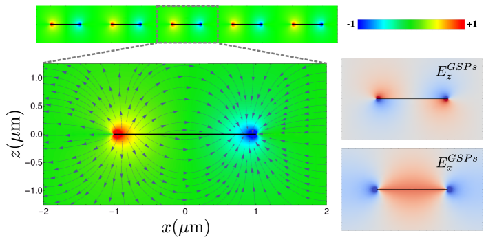
The figure plainly demonstrates the potential graphene plasmons have to squeeze EM fields into deep subwavelength dimensions. Notice that most of the modal energy is concentrated in the immediate vicinity of the graphene ribbons. In addition, the spatial distribution of the electric field is not uniform along the ribbons’ transverse direction: the density of charge-carriers (and thus the electric field) is higher at both edges of the ribbons. The charge-density is also antisymmetric with respect to the ribbons’ midpoint, bearing some similarity to an electric dipole. Such extreme field localization plays a pivotal role, for instance, in biosensing, allowing the detection of minute variations in the local dielectric environment due to the presence/adsorption of a given target analyte. This property, together with ability to tune the GSP-resonances, enables not only unprecedentedly large field overlaps, but also provides a route to tailor the interaction of GSPs with the vibrational resonances of biochemical molecules, thereby achieving huge spectral overlaps that allow specific label-free detection of biomolecules via their vibrational fingerprints.Rodrigo et al. (2015); Farmer et al. (2016)
We further note that the overall spatial configuration of the field illustrated in Fig. 5 is qualitatively maintained throughout a wide range of ribbon widths, from the micrometer to the nanometer size, provided that we are within the quasi-static regime (i.e. ) and at resonant frequencies below , beyond which GSPs become quenched owing to the onset of interband Landau damping.de Abajo (2014); Gonçalves and Peres (2016) This scale-invariance is a property of the electrostatic limit.Christensen et al. (2012); de Abajo (2014); Gonçalves and Peres (2016) Note, however, that we include retardation in our calculations nevertheless.
The results presented above, covering an appreciable vast parameter space, suggest that our analytical model is able to correctly describe the fundamental plasmonic excitations which arise in periodic grids of graphene ribbons. We thus have built an analytic framework which delivered closed-form expressions for the spectra which can be easily evaluated, and that yield results consistent with those found in the literature.Ju et al. (2011); Yan et al. (2013); Bludov et al. (2013); Xiao et al. (2016); Low and Avouris (2014); de Abajo (2014); Gonçalves and Peres (2016)
III.2 THz plasmons in graphene microribbons
In order to determine to what extent our analytical model is capable of explaining experimental spectra, we shall test our theory against measured data taken from the experiments performed by Ju et al.Ju et al. (2011) To that end, we mimic the experimental setup by feeding the reported empirical parameters into our equations. In addition, we concurrently employ a semi-analytical technique introduced elsewherePeres et al. (2012); Bludov et al. (2012); Slipchenko et al. (2013); Bludov et al. (2013); Gonçalves and Peres (2016) which represents the conductivity of graphene (and resultant current) in terms of a Fourier series (see appendix C). This has the advantage of taking into account not only the fundamental plasmonic resonance, but also the higher-order ones. On the other hand, it requires the numerical solution of a linear algebra problem and therefore we refer to it as a semi-analytical method hereafter. We further emphasize that, to the best of our knowledge, so far no attempt has been made to perform a direct comparison of the outcome of this latter method against available experimental data. Nevertheless, it is still far less computationally-demanding than fully numerical simulations such as the FDTD or FEM techniques.A. Bondeson and Ingelström (2005)
In their experiments, the authors of Ref. [Ju et al., 2011] fabricated three different samples containing periodic grids of graphene ribbons with widths of 4, 2 and 1 m, while maintaining the ratio unchanged. Moreover, the authors have concluded that an effective dielectric constant of adequately accounts for the intricate optical constants of the cladding dielectrics (ion gel and SiO2/Si), and have reported a scattering rate of THz.Ju et al. (2011) While at THz frequencies the conductivity of graphene can be approximated by its Drude expression, here we model the conductivity as obtained using the Kubo formula at room temperature (see appendix B). This is necessary here because the experimental data of Ju et al.Ju et al. (2011) refers to the change in transmittance with respect to the same quantity measured at the “charge neutral point” (CNP) [when the Fermi level is at the so-called Dirac point] where neither finite-temperature nor interband processes can be neglected.
The comparison between the calculated GSP-induced (normalized) change in transmittance, , and the experimental data is portrayed in Fig. 6. The observed agreement between theory and experiment is outstanding and constitutes compelling evidence that both theories are capable of interpreting the measured spectra.
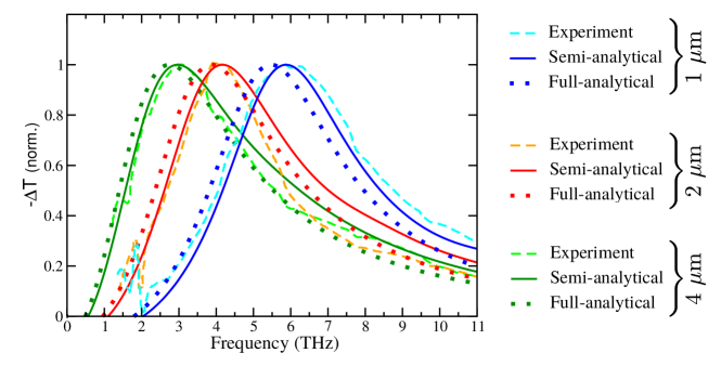
The peaks visible in the figure originate from the excitation of the main GSP plasmonic resonance supported by the graphene ribbons which form the grid. The shifting of the plasmon resonances towards higher frequencies as a consequence of the narrowing of the ribbons exhibits the predicted scaling behavior. Although the degree of accordance between the data and the full-analytical model is rather good, it seems that this model slightly underestimates the resonant frequency. On the other hand, the agreement among the experimental measurements and the spectra obtained by the semi-analytical model is indeed quite remarkable, with the computed (measured) GSP-resonances located at 2.9 (3), 4 (4.1) and 5.6 (6) THz for arrays with ribbon widths of 4, 2 and 1 m, respectively. Therefore, a possible motif for the small redshift visible in the spectra produced by the full-analytic theory may be concerned either with the fact that it neglects the higher-order plasmon resonances and/or to the approximation made for the current involving the edge condition, for instance, it may not be exactly modeled by a square-root as in Eq. (11) [see appendix A.5]. Still, and despite this fact, the fidelity of the analytical model remains very good.
It should be appreciated that the use of either one of the above-mentioned analytical or semi-analytical techniques, apart from requiring less resources, provide a level of physical insight and intuition that numerical methodologies based on the numerical solution of Maxwell’s equations simply cannot envision.
III.3 Hybrid mid-IR plasmons in graphene nanoribbons: plasmon-phonon coupling
Graphene plasmonics has the potential to become a viable tool for nanophotonic devices working within a broad spectral window, from the THz/far-IR up to mid-IR frequencies. Remarkably, routes to bring graphene plasmonics to near-IR and visible frequencies have already been proposed from a theoretical perspectivede Abajo (2014).
At the time of writing, many experiments have reported GSPs at mid-IR frequencies.Rodrigo et al. (2015); Farmer et al. (2016); Luxmoore et al. (2014); Fang et al. (2013, 2014); Brar et al. (2013, 2014); Zhu et al. (2014) Coupling light to graphene plasmons at those frequencies can be realized in nanostructured graphene with typical dimensions from several tens of nanometers to a few hundreds of the nanometer. The mid-IR spectral range is a particularly important one, as many biological and chemical compounds exhibit resonances in that region of the EM spectrum. Thus, tunable graphene plasmons may be perceived as a fertile playground for applications in biochemical sensing and spectroscopy. Furthermore, when graphene is deposited in a polar substrate — such as hBN or SiO2 — the Fuchs–Kliewer SO phononsFuchs and Kliewer (1965) of the substrate can couple to plasmons in graphene via Fröhlich interaction,Mahan (2000) leading to the emergence of new hybrid modes dubbed graphene surface plasmon-phonon polaritonsYan et al. (2013); Brar et al. (2014) (GSPPhs). In order to account for the optical phonons arising in the neighboring polar material(s), their corresponding frequency-dependent, complex-valued dielectric function(s) can be modeled using adequate Lorentz oscillator modelsAshcroft and Mermin (1976) incorporating the phononic resonances, or more evolved models, e.g. based on Gaussian functions and integrals.Kitamura et al. (2007) The hallmark of strong coupling between graphene plasmons and SO phonons is the complete reshaping of the traditional dispersion of bare GSPs into a set of multiple well-defined branches ascribed to hybrid GSPPhs modes possessing mixed plasmonic and phononic character, as demonstrated in Fig. 7-c) for extended graphene sitting on SiO2 (see caption for further details). In particular, notice the evident anti-crossing behavior of the plasmon-phonon bands in the vicinity of the SO frequencies.
In Fig. 7 [panels a) and b)] we compare the results for arrays of graphene ribbons obtained using the analytic [a)] and semi-analytic [b)] methods (solid lines) against the experimental spectra (light-brown points) collected by Luxmoore et al.Luxmoore et al. (2014) Their data shows evidence of strong interaction of GSPs — excited in periodic grids of graphene nanoribbons — with the three SO phonons of the underlying SiO2 substrate. In our modeling, we have met the experimental configuration of the fabricated devices, consisting in doped ( eV) nanoribbons with widths ranging from 450 nm down to 180 nm arranged in a periodic array with periodicity .Luxmoore et al. (2014) The dynamical dielectric function of the SiO2 substrate was taken from the literatureKitamura et al. (2007), and we have employed, as before, the optical conductivity of graphene under Kubo’s framework.
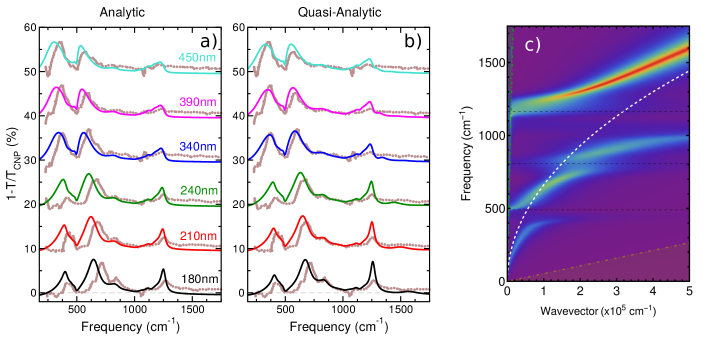
It is worth to highlight that both the analytic and semi-analytic theories outlined above fit admirably to the experimental data, whose structure is now much more intricate than the one seen for microribbons in the THz range. The GSPPh-induced extinction spectrum () of the several samples presented in Fig. 7 reveals the existence of multiple peaks, which correspond to the four polaritonic bands visible in figure’s last panel. We stress that, as expected, all four resonances shift toward higher frequencies upon decreasing ribbon size. Note, however, that they disperse at different rates. This is a direct consequence of the relative plasmon-to-phonon content which tends to vary depending on the distance each resonance is from the SO flat bands: the more plasmon-like the hybrid GSPPhs modes are (i.e. the farther they are from the uncoupled SO bands), the faster they disperse. Another key element, recognizable in the spectra, is the clear transfer of spectral weight from the first peak to the other resonances ascribed to higher GSPPhs bands. Together, the above-mentioned features constitute unambiguous manifestations of anti-crossing behavior.
From the first two panels of Fig. 7 it is apparent that both models closely follow the experimental data, thereby confirming their adequacy to describe the empirical extinction spectra. As in the case of the microribbons, the fully analytical method tends to underestimate slightly the position of the resonances, while the semi-analytical method yields an excellent agreement, particularly for the samples with wider ribbons. The small deviation from the data observed in the spectra of the narrower ribbons may have multiple origins exogenous to our theory, for instance, an incomplete knowledge of the dielectric properties of the particular SiO2 substrate used in the experiments and/or the effect of edge damage (and defects) introduced during the etching processYan et al. (2013); Luxmoore et al. (2014); Han et al. (2007) — which, naturally, should be more pronounced for smaller ribbons —, and may yield ribbon edges with impaired electrical activity (therefore rendering effective widths smaller than the actual ribbon widthsYan et al. (2013)). Here, we neglect the impact of the latter since it has been shown that the damage at the edges of each ribbon is highly heterogeneous.Luxmoore et al. (2014); Han et al. (2007)
The theoretical results produced in this work and subsequent confrontation against experimental data confirm the ability of the theoretical tools developed here to simulate and interpret spectra taken from real-world experiments, providing excellent, reliable results almost instantaneously222Using a standard personal laptop equipped with a dual-core (4 threads) GHz processor. without the need of substantial computational resources.
IV Conclusions
In conclusion, we have developed a novel analytical approach, based on the edge condition and Bloch-expansions for the fields, to describe graphene plasmons excited in periodic grids of graphene ribbons. We solved the scattering problem and provided simple closed-form expressions to compute the reflectance, absorbance, transmittance, and related extinction spectra. We then benchmarked the results of our analytical theory using a semi-analytical model, and tested both techniques against experimental data available in the literature.Ju et al. (2011); Luxmoore et al. (2014) Our results show a very good agreement between the theoretical curves and the empirical data, which constitutes compelling evidence for the validity of the aforementioned theories. That concordance extends from the THz, using microribbon arrays, to the mid-IR spectral region, using nanoribbons. In the latter domain, we have also investigated hybrid GSPPhs excitations that arise from the interaction of GSPs with the SO phonons of the SiO2 substrate, leading to the appearance of four composite modes featuring spectral weight transfer, which is indicative of anti-crossing behavior (resulting from the reconstruction of the bare GSPs spectrum owing the polar coupling).
The approaches developed in this work have two main advantages: (i) they endow us with a deeper insight and sense for the physics governing plasmonic excitations in engineered graphene structures; and, (ii) render viable simulations of experimentally relevant quantities, on-demand and almost instantaneously, without the cost of lengthy, computationally-demanding full-wave numerical packages, at least for patterned structures with a fair degree of symmetry. On the other hand, these naturally cannot compete with fully-numerical techniques such as FEM simulations in what concerns versatility to deal with many different and complex geometries.
Our findings suggest that both the analytical and the semi-analytical models described here could be used to architecture new forefront nanophotonic experiments based on graphene plasmonics, which is emerging as a promising field to deliver cutting-edge optoelectronic devices with tailored light-matter interactions.
Acknowledgements.
The authors thank N. Asger Mortensen for insightful and valuable comments. PADG acknowledges financial support from Fundação para a Ciência e a Tecnologia (Portugal) from grant No. PD/BI/114376/2016. NMRP and YVB acknowledge financial support from the European Commission through the project “Graphene-Driven Revolutions in ICT and Beyond” (Ref. No. 696656). This work was partially supported by the Portuguese Foundation for Science and Technology (FCT) in the framework of the Strategic Financing UID/FIS/04650/2013. The Center for Nanostructured Graphene is sponsored by the Danish National Research Foundation, Project DNRF103.Appendix A
A.1 Convergence of the sum in
Notice that our results for the reflection and transmission amplitudes fundamentally depend on , which in turn strongly depends on the function . The latter reads [cf. Eq. (17)]
| (23) |
where in the last equality we have made explicit use of the fact that the summand is even with respect to , where integers. Note that this expression comprises an infinite sum over , so that we have also truncated the sum in the last step of Eq. (23) for numerical purposes. The question that now arises is: how large should be? And what requirements should it fulfill?
In order to answer these questions, let us plot the results of, say, the reflectance, using several values for . The outcome of such procedure is shown in Fig. 8. From the figure, one can see a striking difference between the results obtained using odd -values and even -values. In particular, note that whenever we picked as odd we always got the same (converged) result. This result also coincides with the one in the limit (light-green curve). Conversely, for even -values, one sees an erratic behavior in the resulting spectra which indicates that the results did not converge. Only for very large values of even (such has 5000), one obtains the correct result. Furthermore, notice that even when choosing a small, but odd value for – such as — one gets the same (correct) result that one would obtain by choosing a large, but even instead — such as . This clearly highlights the need to choose correctly, namely to choose an odd-valued .
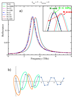
The reason for this apparently counterintuitive behavior can be elucidated by plotting the values of the summand in Eq. (23) as a function of . This is done in panel b) of Fig. 8. Clearly, the figure shows an alternating series; this kind of series usually demands proper care for their accurate computation. In our case, one needs to have special care when choosing , that is, to choose an odd-valued . In that way, the total number of elements of the series is (because it includes the term), which is even, and, therefore, it correctly includes pairs of positive and negative values [as indicated in figure’s 8 panel b)]. Naturally, as approaches infinity, the choice between -odd or -even becomes unimportant. However, our analysis demonstrates that by using an odd-valued , one can obtain accurate results with (odd) -values as small as 5 (this truncation depends naturally on the particular system’s geometry, but in general only a few terms of the sum are needed).
A.2 Derivation of the formulae for the reflectance and transmittance spectra
For the derivation of the reflectance and transmittance scattering probabilities, we need to introduce the Poynting vector (for non-magnetic media),
| (24) |
which characterizes the flux of electromagnetic energy per unit area. Assuming that both and can be written as in terms of harmonic functions, , one may write the time-averaged Poynting vector as
| (25) |
where the star denotes the complex-conjugate. For a TM wave polarized in the -plane, the time-averaged Poynting vector reads
| (26) |
Then, applying the previous equation for the incident wave, one obtains
| (27) |
for the -component (i.e. the component normal to the graphene grating). Similarly, for the reflected wave one has
| (28) |
for the -th diffraction order (or Bloch-mode), whereas for the transmitted wave we obtain
| (29) |
At this point we should stress that for purely imaginary wavevectors, , the Poynting vectors associated with those Bloch modes give zero contribution [since ; cf. Eqs. (28) and (29)], and, as such, they will not contribute neither to the reflectance nor to the transmittance. This is because they are evanescent waves, and therefore they do not carry energy along the -direction. Notice that the modes are so-called non-propagating or evanescent whenever , where with , and , in which case we have
| (30) |
in accordance with the definitions used in the main text. Finally, the reflectance and transmittance through the structure under oblique incidence read
| (31) |
and
| (32) |
respectively, where the sums were carried out over propagating modes only (solely the mode for the parameters used in this work). The absorption spectrum stems from these equations according to .
A.3 Modes contributing to the fundamental resonance for different filling ratios
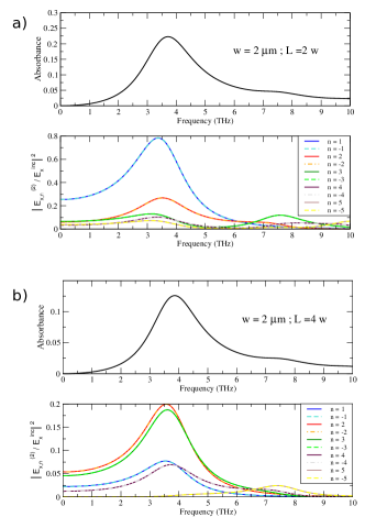
We further note that the particular Bragg modes that couple the most to the fundamental GSP-resonance depend on the specific filling ratio of the system. Such dependence is a consequence of the overlapping of the fields with the ribbon, and, therefore, the geometric configuration (the filling ratio) is an important parameter. As an example, in Fig. 9 (obtained using the semi-analytical method outlined in appendix C) we shown relative modulus-squared Bloch amplitudes corresponding to several Bragg modes, for two different configurations.
A.4 Spectral weight akin to the higher-order multipolar resonances
Figure 10 shows the two lowest-energy plasmonic resonances in the system under study (for different doping levels). Note that, as discussed in the main article, the analytic approach does not account for the higher-order (multi-polar) resonances.
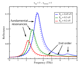
The semi-analytical method, on the other hand, includes these resonances; notice, for instance, the small, weaker peaks at higher frequencies to the right of the fundamental resonance. These, however, carry little spectral weight and can only be seen due to the rather small damping parameter ( meV). This justifies their omission when using the full-analytical technique, as their contribution is rather small.
A.5 Ansatz for the current
Here, we compare the ansatz for the current – cf. Eq. (11) – against the same quantity computed as a Fourier series, as in the semi-analytic method [see Eq. (51)]. Notice that the overall correspondence is quite good, thus providing further evidence for the validity of the edge condition in our fully-analytic framework.
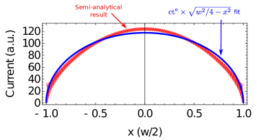
The oscillations emerging in the plot corresponding to the semi-analytic method are a natural consequence of the use of a Fourier expansion to describe the current in such geometry — a feature that is known as Gibbs phenomenon George B. Arfken and Harris (2013). Naturally, these are absent in the analytic ansatz for the current.
Appendix B Dynamical conductivity of graphene
In this work we model the dynamical conductivity of the graphene ribbons using Kubo’s formula within the local approximation at room temperature ( K). In such framework, the material’s 2D conductivity reads Falkovsky (2008); Gonçalves and Peres (2016)
| (40) | ||||
| (41) | ||||
| (42) |
where (here is Boltzmann’s constant), , and where the quantity is defined as
| (43) |
In the THz regime, for graphene under typical doping levels — such that and —, the conductivity of graphene can be well approximated by the Drude-like expression
| (44) |
provided that the conditions and are met.
Appendix C Semi-analytical method in a nutshell
Similarly to the fully-analytical method described in the main text, the semi-analytical method also expresses the EM fields in the form of Bloch-sums.Peres et al. (2012); Bludov et al. (2012); Slipchenko et al. (2013); Bludov et al. (2013); Gonçalves and Peres (2016) Namely, the fields in the medium may be written as (under normal incidence)
| (45) | ||||
| (46) | ||||
| (47) |
where , and . Imposing the adequate boundary conditions, one obtains the following system of equations
| (48) | ||||
| (49) |
for and , respectively, and where . In Eqs. (48) and (49), the quantities are the components of the Fourier series that incorporates the system’s periodicity, that is
| (50) | ||||
| (51) |
The numerical solution of the (truncated) system of equations posed by Eqs. (48) and (49) for each frequency (entering as a parameter), renders the field amplitudes, , in terms of . As before, only the mode with is propagating, and thus only this contributes (i.e. reaches the far-field) to the transmittance, reflectance and absorbance, which read
| (52) | ||||
| (53) | ||||
| (54) |
From these expressions, the corresponding spectra akin to the semi-analytical model may be readily obtained.
References
- Maradudin et al. (2014) A. A. Maradudin, W. L. Barnes, and J. R. Sambles, Modern Plasmonics (Elsevier, 2014).
- Barnes et al. (2003) W. L. Barnes, A. Dereux, and T. W. Ebbesen, Nature 424, 824 (2003).
- Gramotnev and Bozhevolnyi (2010) D. K. Gramotnev and S. I. Bozhevolnyi, Nature Photon. 4, 83 (2010).
- Schuller et al. (2010) J. A. Schuller, E. S. Barnard, W. Cai, Y. C. Jun, J. S. White, and M. L. Brongersma, Nature Materials 9, 193 (2010).
- Armstrong (2012) S. Armstrong, Nature Photonics 6, 720 (2012).
- Ozbay (2006) E. Ozbay, Science 311, 189 (2006).
- Toropov and Shubina (2015) A. A. Toropov and T. V. Shubina, Plasmonic Effects in Metal-Semiconductor Nanostructures (Oxford, 2015).
- Pelton et al. (2008) M. Pelton, J. Aizpurua, and G. Bryant, Laser & Photon. Rev. 2, 136 (2008).
- Pelton and Bryant (2013) M. Pelton and G. W. Bryant, Introduction to Metal-Nanoparticle Plasmonics, 1st ed. (John Wiley & Sons, Inc, New Jersey, 2013).
- Billings (2013) L. Billings, Nature 500, 138 (2013).
- Zheludev and Kivshar (2012) N. I. Zheludev and Y. S. Kivshar, Nature Materials 11, 917 (2012).
- Geim (2009) A. K. Geim, Science 324, 1530 (2009).
- Neto et al. (2009) A. H. C. Neto, F. Guinea, N. M. R. Peres, K. S. Novoselov, and A. K. Geim, Rev. Mod. Phys. 81, 109 (2009).
- Ferrari et al. (2015) A. C. Ferrari et al., Nanoscale 7, 4598 (2015).
- Avouris (2010) P. Avouris, Nano Lett. 10, 4285 (2010).
- Bonaccorso et al. (2010) F. Bonaccorso, Z. Sun, T. Hasan, and A. C. Ferrari, Nature Photonics 4, 611 (2010).
- Grigorenko et al. (2012) A. N. Grigorenko, M. Polini, and K. S. Novoselov, Nature Photonics 6, 749 (2012).
- de Abajo (2014) F. J. G. de Abajo, ACS Photonics 1, 135 (2014).
- Xiao et al. (2016) S. Xiao, X. Zhu, B.-H. Li, and N. A. Mortensen, Front. Phys. 11, 117801 (2016).
- Low and Avouris (2014) T. Low and P. Avouris, ACS Nano 8, 1086 (2014).
- Koppens et al. (2011) F. H. L. Koppens, D. E. Chang, and F. J. G. de Abajo, Nano Lett. 11, 3370 (2011).
- Bludov et al. (2013) Y. V. Bludov, A. Ferreira, N. M. R. Peres, and M. I. Vasilevskiy, Int. J. Mod. Phys. B 27, 1341001 (2013).
- Politano and Chiarello (2014) A. Politano and G. Chiarello, Nanoscale 6, 10927 (2014).
- Gonçalves and Peres (2016) P. A. D. Gonçalves and N. M. R. Peres, An Introduction to Graphene Plasmonics (World Scientific, Singapore, 2016).
- Khurgin and Boltasseva (2012) J. B. Khurgin and A. Boltasseva, MRS Bulletin 37, 768 (2012).
- Rodrigo et al. (2015) D. Rodrigo, O. Limaj, DavideJanner, D. Etezadi, F. J. G. de Abajo, V. Pruneri, and H. Altug, Science 349, 165 (2015).
- Farmer et al. (2016) D. B. Farmer, P. Avouris, Y. Li, T. F. Heinz, and S.-J. Han, ACS Photonics 3, 553 (2016).
- Wang et al. (2013) P. Wang, O. Liang, W. Zhang, T. Schroeder, and Y.-H. Xie, Advanced Materials 25, 4918 (2013).
- Zeng et al. (2015) S. Zeng, S. Hu, J. Xia, T. Anderson, X.-Q. Dinh, X.-M. Meng, P. Coquet, and K.-T. Yong, Sensors and Actuators B: Chemical 207, 801 (2015).
- Zhao et al. (2013) Y. Zhao, X. Hu, G. Chen, X. Zhang, Z. Tan, J. Chen, R. S. Ruoff, Y. Zhu, and Y. Lu, Phys. Chem. Chem. Phys. 15, 17118 (2013).
- Ling et al. (2010) X. Ling, L. Xie, Y. Fang, H. Xu, H. Zhang, J. Kong, M. S. Dresselhaus, J. Zhang, and Z. Liu, Nano Lett. 10, 553 (2010).
- Xu et al. (2012) W. Xu, X. Ling, J. Xiao, M. S. Dresselhaus, J. Kong, H. Xu, Z. Liu, and J. Zhang, Proceedings of the National Academy of Sciences 109, 9281 (2012).
- Zhao et al. (2014) Y. Zhao, G. Chen, Y. Du, J. Xu, S. Wu, Y. Qu, and Y. Zhu, Nanoscale 6, 13754 (2014).
- Liu et al. (2011a) C.-Y. Liu, K.-C. Liang, W. Chen, C. hao Tu, C.-P. Liu, and Y. Tzeng, Opt. Express 19, 17092 (2011a).
- Heeg et al. (2013) S. Heeg, R. Fernandez-Garcia, A. Oikonomou, F. Schedin, R. Narula, S. A. Maier, A. Vijayaraghavan, and S. Reich, Nano Lett. 13, 301 (2013).
- Urich et al. (2012) A. Urich, A. Pospischil, M. M. Furchi, D. Dietze, K. Unterrainer, and T. Mueller, Appl. Phys. Lett. 101, 153113 (2012).
- Bao et al. (2011) Q. Bao, H. Zhang, B. Wang, Z. Ni, C. H. Y. X. Lim, Y. Wang, D. Y. Tang, and K. P. Loh, Nature Photonics 5, 411 (2011).
- Sorger et al. (2015) C. Sorger, S. Preu, J. Schmidt, S. Winnerl, Y. V. Bludov, N. M. R. Peres, M. I. Vasilevskiy, and H. B. Weber, New J. Phys. 17, 053045 (2015).
- Sun et al. (2016a) Z. Sun, A. Martinez, and F. Wang, Nature Photonics 10, 227 (2016a).
- Sensale-Rodriguez et al. (2012) B. Sensale-Rodriguez, R. Yan, M. Zhu, D. Jena, L. Liu, and H. Grace Xing, Appl. Phys. Lett. 101, 261115 (2012).
- Yu et al. (2015) R. Yu, V. Pruneri, and F. J. G. de Abajo, ACS Photonics 2, 550 (2015).
- Sensale-Rodriguez et al. (2013) B. Sensale-Rodriguez, S. Rafique, R. Yan, M. Zhu, V. Protasenko, D. Jena, L. Liu, and H. G. Xing, Opt. Express 21, 2324 (2013).
- Fang et al. (2012a) Z. Fang, Z. Liu, Y. Wang, P. M. Ajayan, P. Nordlander, and N. J. Halas, Nano Lett. 12, 3808 (2012a).
- Liu et al. (2011b) Y. Liu, R. Cheng, L. Liao, H. Zhou, J. Bai, G. Liu, L. Liu, Y. Huang, and X. Duan, Nature Communications 2 (2011b).
- Sun et al. (2016b) Z. Sun, L. Aigouy, and Z. Chen, Nanoscale 8, 7377 (2016b).
- Echtermeyer et al. (2016) T. J. Echtermeyer, S. Milana, U. Sassi, A. Eiden, M. Wu, E. Lidorikis, and A. Ferrari, Nano Lett. 16, 8 (2016).
- Koppens et al. (2014) F. H. L. Koppens, T. Mueller, P. Avouris, A. C. Ferrari, M. S. Vitiello, and M. Polini, Nature Nanotechnology 9, 780 (2014).
- Ju et al. (2011) L. Ju, B. Geng, J. Horng, C. Girit, M. Martin, Z. Hao, H. A. Bechtel, X. Liang, A. Zettl, Y. R. Shen, and F. Wang, Nature Nanotechnology 6, 630 (2011).
- Yan et al. (2013) H. Yan, T. Low, W. Zhu, Y. Wu, M. Freitag, X. Li, F. Guinea, P. Avouris, and F. Xia, Nature Photonics 7, 394 (2013).
- Nene et al. (2014) P. Nene, J. H. Strait, W.-M. Chan, C. Manolatou, J. W. Kevek, S. Tiwari, P. L. McEuen, and F. Rana, Appl. Phys. Lett. 105, 143108 (2014).
- Yan et al. (2012a) H. Yan, X. Li, B. Chandra, G. Tulevski, Y. Wu, M. Freitag, W. Zhu, P. Avouris, and F. Xia, Nature Nanotechnology 7, 330 (2012a).
- Luxmoore et al. (2014) I. J. Luxmoore, C. H. Gan, P. Q. Liu, F. Valmorra, P. Li, J. Faist, and G. R. Nash, ACS Photonics 1, 1151 (2014).
- Hu et al. (2015) H. Hu, F. Zhai, D. Hu, Z. Li, B. Bai, X. Yang, and Q. Dai, Nanoscale 7, 19493 (2015).
- Yan et al. (2012b) H. Yan, F. Xia, Z. Li, and P. Avouris, New J. Phys. 14, 125001 (2012b).
- Fang et al. (2013) Z. Fang, S. Thongrattanasiri, A. Schlather, Z. Liu, L. Ma, Y. Wang, P. M. Ajayan, P. Nordlander, N. J. Halas, and F. J. G. de Abajo, ACS Nano 7, 2388 (2013).
- Fang et al. (2014) Z. Fang, Y. Wang, A. E. Schlather, Z. Liu, P. M. Ajayan, F. J. G. de Abajo, P. Nordlander, X. Zhu, and N. J. Halas, Nano Lett. 14, 299 (2014).
- Zhu et al. (2014) X. Zhu, W. Wang, W. Yan, M. B. Larsen, P. Boeggild, T. G. Pedersen, S. Xiao, J. Zi, and N. A. Mortensen, Nano Lett. 14, 2907 (2014).
- Liu et al. (2015) P. Q. Liu, F. Valmorra, C. Maissen, and J. Faist, Optica 2, 135 (2015).
- Yeung et al. (2014) K. Y. M. Yeung, J. Chee, H. Yoon, Y. Song, J. Kong, and D. Ham, Nano Lett. 14, 2479 (2014).
- Brar et al. (2013) V. W. Brar, M. S. Jang, M. Sherrott, J. J. Lopez, and H. A. Atwater, Nano Lett. 13, 2541 (2013).
- Brar et al. (2014) V. W. Brar, M. S. Jang, M. Sherrott, S. Kim, J. J. Lopez, L. B. Kim, M. Choi, and H. Atwater, Nano Lett. 14, 3876 (2014).
- Yao et al. (2013) Y. Yao, M. A. Kats, P. Genevet, N. Yu, Y. Song, J. Kong, and F. Capasso, Nano Lett. 13, 1257 (2013).
- Fang et al. (2012b) Z. Fang, Y. Wang, Z. Liu, A. Schlather, P. M. Ajayan, F. H. L. Koppens, P. Nordlander, and N. J. Halas, ACS Nano 6, 10222 (2012b).
- Alonso-González et al. (2014) P. Alonso-González et al., Science 344, 1369 (2014).
- Gao et al. (2013) W. Gao, G. Shi, Z. Jin, J. Shu, Q. Zhang, R. Vajtai, P. M. Ajayan, J. Kono, and Q. Xu, Nano Lett. 13, 3698 (2013).
- Zhu et al. (2013) X. Zhu, W. Yan, P. Uhd Jepsen, O. Hansen, N. Asger Mortensen, and S. Xiao, Appl. Phys. Lett. 102, 131101 (2013).
- Fei et al. (2011) Z. Fei et al., Nano Lett. 11, 4701 (2011).
- Yan et al. (2012c) H. Yan, Z. Li, X. Li, W. Zhu, P. Avouris, and F. Xia, Nano Lett. 12, 3766 (2012c).
- Constant et al. (2015) T. J. Constant, S. M. Hornett, D. E. Chang, and E. Hendry, Nature Physics 11, 1 (2015).
- Tokman et al. (2016) M. Tokman, Y. Wang, I. Oladyshkin, A. R. Kutayiah, and A. Belyanin, Phys. Rev. B 93, 235422 (2016).
- Fei et al. (2012) Z. Fei et al., Nature 487, 82 (2012).
- Chen et al. (2012) J. Chen et al., Nature 487, 77 (2012).
- Woessner et al. (2015) A. Woessner et al., Nature Materials 14, 421 (2015).
- Barcelos et al. (2015) I. D. Barcelos, A. R. Cadore, L. C. Campos, A. Malachias, K. Watanabe, T. Taniguchi, F. C. B. Maia, R. Freitas, and C. Deneke, Nanoscale 7, 11620 (2015).
- Peres et al. (2012) N. M. R. Peres, A. Ferreira, Y. V. Bludov, and M. I. Vasilevskiy, J. Phys.: Condens. Matter 24, 245303 (2012).
- Bludov et al. (2012) Y. V. Bludov, N. M. R. Peres, and M. I. Vasilevskiy, Phys. Rev. B 85, 245409 (2012).
- Slipchenko et al. (2013) T. M. Slipchenko, M. L. Nesterov, L. Martin-Moreno, and A. Y. Nikitin, J. Opt. 15, 114008 (2013).
- Thongrattanasiri et al. (2012) S. Thongrattanasiri, A. Manjavacas, and F. J. G. de Abajo, ACS Nano 6, 1766 (2012).
- Christensen et al. (2014) T. Christensen, W. Wang, A.-P. Jauho, M. Wubs, and N. A. Mortensen, Phys. Rev. B 90, 241414 (2014).
- Abramowitz and Stegun (1965) M. Abramowitz and I. A. Stegun, Handbook of Mathematical Functions: with Formulas, Graphs, and Mathematical Tables (Dover, New York, 1965).
- Barkeshli (2015) K. Barkeshli, Advanced Electromagnetics and Scattering Theory (Springer, New York, 2015).
- Mikhailov and Savostianova (2005) S. A. Mikhailov and N. A. Savostianova, Phys. Rev. B 71, 035320 (2005).
- Kotov et al. (2012) V. N. Kotov, B. Uchoa, V. M. Pereira, F. Guinea, and A. H. Castro Neto, Rev. Mod. Phys. 84, 1067 (2012).
- Li et al. (2008) Z. Q. Li, E. A. Henriksen, Z. Jiang, Z. Hao, M. C. Martin, P. Kim, H. L. Stormer, and D. N. Basov, Nature Physics 4, 532 (2008).
- Note (1) The fitting function was obtained using the least-squares method.
- Christensen et al. (2012) J. Christensen, A. Manjavacas, S. Thongrattanasiri, F. H. L. Koppens, and F. J. G. de Abajo, ACS Nano 6, 431 (2012).
- A. Bondeson and Ingelström (2005) T. R. A. Bondeson and P. Ingelström, Computational Electromagnetics (Springer, New York, 2005).
- Fuchs and Kliewer (1965) R. Fuchs and K. L. Kliewer, Phys. Rev. 140, A2076 (1965).
- Mahan (2000) G. D. Mahan, Many-Particle Physics, 3rd ed. (Springer, New York, 2000).
- Ashcroft and Mermin (1976) N. W. Ashcroft and N. D. Mermin, Solid State Physics, 1st ed. (Saunders College, New York, 1976).
- Kitamura et al. (2007) R. Kitamura, L. Pilon, and M. Jonasz, Appl. Opt. 46, 8118 (2007).
- Han et al. (2007) M. Y. Han, B. Özyilmaz, Y. Zhang, and P. Kim, Phys. Rev. Lett. 98, 206805 (2007).
- Note (2) Using a standard personal laptop equipped with a dual-core (4 threads) GHz processor.
- George B. Arfken and Harris (2013) H. J. W. George B. Arfken and F. E. Harris, Mathematical Methods for Physicists, 7th ed. (Elsevier, New York, 2013).
- Falkovsky (2008) L. A. Falkovsky, J. Phys.: Conf. Ser. 129, 012004 (2008).