Direct Detection of sub-GeV Dark Matter with Scintillating Targets
Abstract
We describe a novel search for MeV-to-GeV-mass dark matter, in which the dark matter scatters off electrons in a scintillating target. The excitation and subsequent de-excitation of the electron produces one or more photons, which could be detected with an array of cryogenic low-noise photodetectors, such as transition edge sensors (TES) or microwave kinetic inductance devices (MKID). Scintillators may have distinct advantages over other experiments searching for a low ionization signal from sub-GeV DM. First, the detection of one or a few photons may be technologically easier. Second, since no electric field is required to detect the photons, there may be far fewer dark counts mimicking a DM signal. We discuss various target choices, but focus on calculating the expected dark matter-electron scattering rates in three scintillating crystals, sodium iodide (NaI), cesium iodide (CsI), and gallium arsenide (GaAs). Among these, GaAs has the lowest band gap (1.52 eV) compared to NaI (5.9 eV) or CsI (6.4 eV), allowing it to probe dark matter masses possibly as low as MeV, compared to MeV with NaI or CsI. We compare these scattering rates with those expected in silicon (Si) and germanium (Ge). The proposed experimental concept presents an important complementary path to existing efforts, and its potential advantages may make it the most sensitive direct-detection probe of DM down to MeV masses.
I INTRODUCTION
Dark matter (DM) with a mass in the MeV–GeV range is phenomenologically viable and has received increasing attention in recent years Essig et al. (2012a, 2016); Graham et al. (2012); Lee et al. (2015); Essig et al. (2012b); Hochberg et al. (2016a); *Hochberg:2015fth; *Schutz:2016tid; *Hochberg:2016ntt; Essig et al. (2013a); *Bird:2004ts; *Borodatchenkova:2005ct; *McElrath:2005bp; *Fayet:2006sp; *Bird:2006jd; *Kahn:2007ru; *Fayet:2007ua; *Essig:2009nc; *Bjorken:2009mm; *Reece:2009un; *Fayet:2009tv; *Yeghiyan:2009xc; *Badin:2010uh; *Echenard:2012iq; *MarchRussell:2012hi; *Essig:2013vha; *Essig:2013goa; *Boehm:2013jpa; *Nollett:2013pwa; *Andreas:2013lya; *Izaguirre:2013uxa; *Battaglieri:2014qoa; *Izaguirre:2014bca; *Batell:2014mga; *Kahn:2014sra; *Krnjaic:2015mbs; *Batell:2009di; *Izaguirre:2015yja; Boehm and Fayet (2004); *Strassler:2006im; *ArkaniHamed:2008qn; *Pospelov:2008jd; *Hooper:2008im; *Feng:2008ya; *Morrissey:2009ur; *Essig:2010ye; *Cohen:2010kn; *Lin:2011gj; *Chu:2011be; *Hochberg:2014dra; *Hochberg:2014kqa. An important probe for DM is with direct detection experiments, in which a DM particle in the Milky-Way halo interacts with some target material in a detector, producing an observable signal in the form of heat, phonons, electrons, or photons Cushman et al. (2013). The traditional technique of searching for nuclear recoils loses sensitivity rapidly for DM masses below a few GeV, since the DM is unable to transfer enough of its energy to the nucleus, resulting in no observable signal above detector thresholds. However, DM scattering off electrons, whose mass is much less than a nucleus, can lead to observable signals for masses well below 1 GeV Essig et al. (2012a), opening up vast new regions of parameter space for experimental exploration.
DM-electron scattering in direct detection experiments has been investigated for noble liquid targets Essig et al. (2012a, b) and was demonstrated explicitly to have sensitivity down to DM masses of a few MeV and cross-sections of Essig et al. (2012b) using published XENON10 data Angle et al. (2011). Semiconductor targets like silicon (Si) and germanium (Ge) could probe potentially several orders of magnitude of unexplored DM parameter space for masses as low as a few hundred keV Essig et al. (2012a); Graham et al. (2012); Lee et al. (2015); Essig et al. (2016). The feasibility of the required detector technology to detect small ionization signals still needs to be demonstrated and may become available in the next few years, e.g. with SuperCDMS Agnese et al. (2016) and DAMIC Fernandez Moroni et al. (2012). In the future, even lower masses could be probed using superconductors or superfluids Hochberg et al. (2016a, 2015a); Schutz and Zurek (2016).
In this letter, we explore using a scintillator as the target material to search for dark matter with masses as low as a few hundred keV. One or more scintillation photons are emitted when an electron excited by a DM-electron scattering interaction relaxes to the ground state Essig et al. (2012a)111Note that Starkman:1994gf proposed the search of one or more photons from Weak-scale dark matter through atomic excitations.. Scintillation photons with an energy of (few eV) could be detected by an array of transition edge sensors (TES) or microwave kinetic inductance detectors (MKIDs) operated at cryogenic temperatures, which surround a scintillating target of volume . The development of such a large array of photodetectors sensitive to single photons is an active area of research Pyle . The target itself should be cooled to cryogenic temperatures to avoid excitations induced by thermal fluctuations and large thermal gradients between it and the detector array.
Several good scintillating materials exist. In this letter, we focus on three crystals, sodium iodide (NaI), cesium iodide (CsI), and gallium arsenide (GaAs). Other materials will be mentioned briefly.
II SCINTILLATORS: ADVANTAGES & CHALLENGES
Several signals are possible when sub-GeV DM scatters off a bound electron in an atom or a crystal, exciting the electron to a higher energy level or an unbound state Essig et al. (2012a). Depending on the target material, an experiment can either measure an ionization signal, which is obtained by manipulating the electron with an electric field, or one or more scintillation photons, which are emitted as the electron relaxes back to its ground state. Until now, the latter approach has not been considered in detail.
Measuring the ionization signal has already constrained DM as light as a few MeV Essig et al. (2012b), using XENON10’s two-phase xenon time projection chamber (TPC). Unfortunately, several possible detector-specific backgrounds exist, so one cannot currently claim that the observed one- and few-electron events are from DM Essig et al. (2012b); Angle et al. (2011); Aprile et al. (2016a). Using semiconductors, CDMSlite Agnese et al. (2016) applied a bias voltage, forcing a conduction-band electron to traverse the material and generate enough Neganov-Luke phonons Luke et al. (1990); Neganov and Trofimov (1985) to be measured by phonon detectors. The CDMSlite setup with improved phonon detectors may in the future surpass xenon-based TPCs in their sensitivity to sub-GeV DM. However, while there may be fewer dark counts than for two-phase xenon TPCs, the presence of an electric field may create spontaneous electron-hole pairs that could mimic a DM signal. Therefore, more work is needed to establish the potential of the CDMSlite setup.
Sub-GeV DM searches are unlikely to be limited by traditional backgrounds like Compton scattering, cosmogenics, or neutrons. These backgrounds typically produce electron recoils at higher energies, and event/kg/year is expected in SuperCDMS in the eV range Golwala (2016). Great care must be taken to limit the material’s surface exposure and radioactive contaminants. Coherent nuclear scattering of solar neutrinos is similarly insignificant. Instead, the discussion above highlights that understanding and controlling detector dark counts will likely determine the sensitivity.
Instead of searching for an ionization signal, one could search for one or more scintillation photons. Scintillators possibly have two distinct advantages. First, the detection of such a low number of photons may turn out to be technologically easier than detecting a low number of electrons with the CDMSlite setup (or with the DAMIC setup Fernandez Moroni et al. (2012)). Second, no electric field is required to detect the photons, which may lead to fewer dark counts.
A potential background for scintillators is phosphorescence induced from a previous interaction (afterglow). Our candidate targets scintillate on nano-to-millisecond timescales, but some photons could arise from excited states whose lifetimes are much longer (phosphorescent) due to a “forbidden” radiative transition. The phosphorescent photons typically have a lower energy, so if the photodetector’s energy resolution is too low, a narrow-band optical filter could be placed between scintillator and photodetector to remove phosphorescent photons.
III SCHEMATIC EXPERIMENTAL CONCEPT
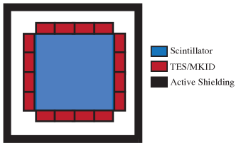
Fig. 1 shows the experimental concept: a scintillating target is surrounded by a detector-array sensitive to single photons. An active shield surrounds the detector to veto radioactive backgrounds, including gamma rays that Compton-scatter in the target material. An optical filter between the scintillator and the photodetector could ensure passage of only the expected photon wavelengths.
Detectors with single-photon sensitivity and no dark counts exist, e.g. MKIDs Mazin et al. (2012) and TESs Irwin and Hilton (2005), which operate at (100 mK) temperatures. These detectors can have few-percent energy resolution and microsecond time resolution Mazin et al. (2012). MKIDs (TESs) have demonstrated single-photon sensitivity at photon energies of eV Mazin et al. (2012) ( eV Petroff et al. (1987)), with the potential to be sensitive to meV phonon energies Santavicca et al. (2010); Hochberg et al. (2015a). Currently the most sensitive single-photon devices Karasik et al. (2012); Goldie et al. (2011); Miller et al. (2003); Hochberg et al. (2015a) are small in size, , but efforts exist to enlarge them Pyle . CRESST-II currently has the best detector of few-cm size, sensitive to photons, which uses a TES read out by SQUIDs Angloher et al. (2016a, b). Silicon photomultipliers (SiPM) are possible photodetectors and operate well at cryogenic temperatures, but the dark-count rate may be too large Biroth et al. (2015); Achenbach et al. (2016).
IV DISTINGUISHING SIGNAL FROM BACKGROUNDS
A few handles exist to distinguish a DM signal from a background. First, the signal rate modulates annually and daily due to the motion of the Earth Drukier et al. (1986). The modulation is larger than for elastic WIMP-nucleus recoils, since the scattering is inelastic Tucker-Smith and Weiner (2001), and increases with threshold. Backgrounds are not expected to have the same phase, amplitude, period, and energy dependence. Second, the DM-induced electron-recoil spectrum is distinctive and unlikely to be mimicked by a background. Third, the DM signal scales with the target volume, in contrast to many potential backgrounds arising from the surrounding detector package. This can be confirmed by using the same detector but with a hollow crystal 222We acknowledge Matthew Pyle for insightful discussions.. Backgrounds that scale with the target volume, such as external gammas and phosphorescence, can be determined by measuring the change in signal when a gamma ray source is placed outside the detector.
V DARK MATTER-ELECTRON SCATTERING
To inform our choice of scintillating materials, we review here the scattering of sub-GeV DM off a bound electron in a crystal. The salient features emphasized below also apply to atoms. See Essig et al. (2016) for details.
The rate for DM-electron scattering to excite an electron from level to is
| (1) | |||
where is the fine-structure constant, () denotes the DM (electron) mass, GeV/cm3 is the local DM density, is the total energy deposited, is the DM-to-electron momentum transfer, is the number of unit cells in the target crystal of total (cell) mass (), and is the DM-electron reduced mass. The crystal form-factor is
| (2) | ||||
where , is the volume of the unit cell, are wavevectors in the first Brillouin Zone (BZ), and is the reciprocal lattice vector. The reference cross-section and DM form factor are parameterizations of the DM-electron interaction defined as
| (3) | |||||
| (4) |
where is the absolute value squared of the elastic DM-free-electron scattering matrix element, averaged over initial-, and summed over final-state particle spins. The DM-halo profile is
| (5) | |||||
where in Eq. (5) we chose for the standard Maxwell-Boltzmann distribution with a sharp cutoff. We take km/s, the Earth velocity about the galactic center km/s, and the DM escape velocity from the galaxy as km/s. is the normalization factor. The minimum velocity required for scattering is
| (7) |
There are four salient features worth emphasizing for sub-GeV DM scattering off electrons:
-
•
First, since the bound electron’s momentum can be arbitrarily high (albeit with suppressed probability), can be arbitrarily high, so that in principle all of the DM’s kinetic energy can be transferred to the electron (in sub-GeV DM scattering off nuclei only a fraction is transferred to a much heavier nucleus). Thus, implies for . Therefore, smaller ionization energies or band gaps can probe lower DM masses, with crystal targets being sensitive down to a few hundred keV.
-
•
Second, since the electron moves at a speed of , much faster than the DM (), the electron determines the typical , . A rough estimate for is the crystal momentum, keV, where is the lattice constant for our target choices (see below). Since , the minimum to obtain a particular is given by . A similar estimate holds for atoms Essig et al. (2016). The signal rate is thus larger in semiconductors with low band gaps ( eV) than insulators ( eV) or noble liquids (, 16, 25 eV for xenon, argon, helium, respectively).
-
•
Third, while the value of is naturally , can in fact be much larger as mentioned above. This allows for much larger momentum transfers and recoil energies, although these are strongly suppressed.
-
•
Fourth, since the scattering is inelastic, the annual modulation of the signal rate is larger than for typical WIMP elastic scattering Tucker-Smith and Weiner (2001).
VI SCINTILLATING TARGETS
The previous discussion suggests using scintillating crystals with low band gaps. However, the crystals must also have high purity, high radiative efficiency (i.e. little non-radiative recombination of excited electron-hole pairs), and few native defects, all while being grown to large sizes ( kg). We thus focus on NaI and CsI, but include GaAs, which may also satisfy these criteria. Table 1 (top) lists salient features.
NaI and CsI are insulators that scintillate efficiently through the decay of self-trapped excitons. They are used extensively due to their high light output and ease of production Moszynski et al. (2005a); ADAMS and DAMS (1970); Hofstadter (1949a, b); Sai ; Moszyriski et al. (2008); Sailer et al. (2012); Mikhailik et al. (2015). Pure CsI is being considered for a DM-nucleus-recoil search Angloher et al. (2016b). Early measurements of GaAs, a direct-gap semiconductor, showed a radiative efficiency (internal) of at 77 K when doped with donors or acceptors Cusano (1964). Conventional coupling to photodetectors is inefficient due to the high refractive index () but one could apply photonic coatings or deposit the photodetectors directly onto the surfaces of the GaAs crystal to reduce internal reflection Knapitsch and Lecoq (2014).
| Material | [eV] | Rad. Eff. | [eV] | [ns] | Mechanism |
|---|---|---|---|---|---|
| NaI Moszynski et al. (2002) | 5.9 | 0.95 | 4.1 | 300 | SX |
| CsI Moszynski et al. (2005a); Amsler et al. (2002) | 6.4 | 4.0 | SX | ||
| GaAs Cusano (1964) | 1.52 | (a) | BE |
| Material | [eV] | Rad. Eff. | [eV] | [ns] | Mechanism |
|---|---|---|---|---|---|
| PVT Trilling (1970) | 4.8 | 0.10 | 3.0 | 2 | organic |
| CaWO4 Zdesenko et al. (2005) | 4.2 | 0.21 | 2.9 | 8000 | CX |
| Xe Aprile et al. (2009); Chepel and Araujo (2013) | 0.30 | 7.1 | 30(c) | excimers | |
| Ar Dehmer and Pratt (1982); Chepel and Araujo (2013) | 0.40 | 9.9 | (c) | excimers | |
| He Guo and McKinsey (2013) | 0.29 | 15.5 | 10(d) | excimers | |
| NaI:Tl de Haas and Dorenbos (2008)(e) | 5.9 | 0.50 | 3.0 | 115 | Tl+ |
| CsI:Tl de Haas and Dorenbos (2008)(e) | 6.4 | 2.2 | 980 | Tl+ |
| Material | [eV] |
|---|---|
| Si | 0.67 |
| Ge | 1.1 |
Other scintillator targets are possible, but not considered further (Table 1, middle). Plastic scintillators, e.g. PVT, have a low radiative efficiency, but this may be offset by their low production cost. CaWO4 also has a low radiative efficiency Moszynski et al. (2005b). Noble liquids can be scaled up relatively easily to large masses. At room temperature, phonons reduce radiative relaxation (i.e. quenching) in NaI and CsI, and Tl+ doping is commonly used to provide efficient radiative centers. We include them to compare with the undoped cases. All listed materials (except PVT) are used for DM-nuclear recoil searches Angloher et al. (2009, 2016a); Aprile et al. (2016a); Akerib et al. (2016); Abe et al. (2013); Aprile et al. (2016b); Akerib et al. (2015); Aalseth et al. (2015); Guo and McKinsey (2013); Bernabei et al. (2010); Froborg (2016); Barbosa de Souza et al. (2016); Lee et al. (2007), but the photodetectors are not sensitive to single photons 333DM-electron scattering in e.g. xenon TPCs could produce two photons in a multi-step de-excitation process. However the efficiency to detect a photon is low (e.g. in LUX). Moreover, the PMTs are not sensitive to the second photon, which is in the infrared..
Other suitable low band gap materials may exist. Crystals with band gaps are likely semiconductors Derenzo et al. (2006). Among these, direct-gap semiconductors have a high radiative efficiency, but no obvious candidates exist besides GaAs. Indirect-gap semiconductors are more common, but their scintillation is slow and inefficient without doping. However, luminescence has been reported from Si Steger et al. (2011); Davies (1994) and Ge Davies et al. (1992) at cryogenic temperatures (Table 1, bottom). More research could reveal suitable dopants to achieve high radiative efficiency. We show results for Ge and Si below since they are potential scintillators and are also used in current experiments sensitive to an ionization signal, like SuperCDMS and DAMIC.
The supplementary materials will review the scintillation mechanisms of the substances in Table 1.
| (bohr) | (bohr3) | ||||
| CsI | 8.6868 | 655.51 | 80 | ||
| NaI | 12.927 | 464.88 | 50 | ||
| GaAs | 10.8690 | 321.00 | 60 | ||
| Ge | 10.8171 | 316.4269 | 66 | 1 243 | |
| Si | 10.3305 | 275.6154 | 56 | 1 243 |
VII CALCULATIONS
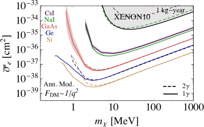
We calculate the DM-electron scattering rates in NaI, CsI, and GaAs using the QEdark module developed in Essig et al. (2016). We use PBE functionals Perdew et al. (1996), norm-conserving pseudopotentials Hamann et al. (1979), and adjust the band gaps to the values in Table 1 using a scissor correction Levine and Allan (1989, 1991). Table 2 lists the required calculation parameters. We include in the density functional theory (DFT) calculation all electrons with binding energies as low as the -shell of Ga (binding energy eV), the - and -shell electrons ( eV and eV, respectively) of Cs, and the -shell electrons of Ge as in Essig et al. (2016); Lee et al. (2015) (deeper electrons are irrelevant). The numerical uncertainty is estimated by choosing 30 random -point meshes. The sensitivity lines for Ge and Si are from Essig et al. (2016) (only one mesh is shown, but the uncertainty is small Essig et al. (2016)).
Our calculations do not include exciton effects. In the supplementary materials, we argue that exciton effects are negligible for the low-gap materials GaAs, Ge, or Si, and may have an effect for NaI and CsI.
VIII RESULTS
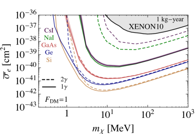
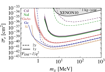
Fig. 2 (left) shows the potential sensitivity to (Eq. (3)) for two different (Eq. (4)), various materials, two thresholds, and data taken over one year with 1 kg of material. We assume a radiative efficiency of 1. The low-gap materials GaAs, Si, and Ge can reach potentially DM masses as low as a few hundred keV, whereas the reach of NaI and CsI is 1–2 MeV. This could probe lower masses than XENON10 Essig et al. (2012b), and extend the high-mass reach by one to several orders of magnitude.
The signal in GaAs, NaI, and CsI consists of one or more photons, while in Ge and Si it consists of either one or more electrons, or (if suitable dopants can provide a high radiative efficiency) one or more photons. We show two thresholds: “” requires , while “” requires , where is the mean energy needed for the recoiling electron to form another electron-hole pair. A phenomenological approach gives eV (3.6 eV, 4.2 eV) for Ge (Si, GaAs) Klein (1968); Knoll (2010); Essig et al. (2016). Precise values for CsI and NaI are unavailable, so we show Knoll (2010). More theoretical work and an experimental calibration can better quantify the number of photons produced by low-energy electron recoils. The mass threshold is different for the and lines. However, the low-gap materials have a similar high-mass reach for either threshold, since is typically several eV and more likely to produce two rather than one photon. Resolving two photons in coincidence can help reduce backgrounds.
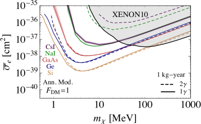
The annual modulation of the signal rate can be used as a discriminant from background Drukier et al. (1986). Fig. 2 (right) shows discovery lines for which with . Here is the modulation amplitude and () is the total number of signal (background) events. The sensitivity weakens , assuming is constant in time.
To summarize, we described a novel search for sub-GeV DM, using scintillators. Scintillators provide a complementary path with potential advantages over other approaches searching for a low ionization signal: the detection of photons may be technologically easier with fewer dark counts.
IX Acknowledgments
We are grateful to Matthew Pyle for numerous insightful discussions, including discussing potential backgrounds (like afterglow), and for suggesting how these could be characterized. We are also grateful to Jeremy Mardon and Tomer Volansky for numerous stimulating conversations. We thank Philip Allen, Jeremy Mardon, and Matthew Pyle for comments on a draft of this manuscript. We have benefited from many useful conversations with Thomas Allison, Mariví Fernández-Serra, Eden Figueroa, Enectali Figueroa-Feliciano, Lauren Hsu, Mark Hybertsen, Serge Luryi, Aaron Manalaysay, Ben Mazin, Daniel McKinsey, Laszlo Mihaly, Florian Reindl, Karoline Schäffner, and Craig Woody. R.E. is supported by the DoE Early Career research program DESC0008061 and through a Sloan Foundation Research Fellowship. T.-T.Y. is also supported by grant DESC0008061. A.M. acknowledges support from NSF grant PHY1316617. A.S. acknowledges support from DoE grant DE-FG02-09ER16052. S.D. acknowledges support from the U.S. Department of Homeland Security, Domestic Nuclear Detection Office. This research used resources of the National Energy Research Scientific Computing Center, a DoE Office of Science User Facility supported by the Office of Science of the U.S. Department of Energy under Contract No. DE-AC02-05CH11231 and the Handy and LIred computer clusters at the Stony Brook University Institute for Advanced Computational Science.
References
- Essig et al. (2012a) R. Essig, J. Mardon, and T. Volansky, Phys. Rev. D85, 076007 (2012a), arXiv:1108.5383 [hep-ph] .
- Essig et al. (2016) R. Essig, M. Fernandez-Serra, J. Mardon, A. Soto, T. Volansky, and T.-T. Yu, JHEP 05, 046 (2016), arXiv:1509.01598 [hep-ph] .
- Graham et al. (2012) P. W. Graham, D. E. Kaplan, S. Rajendran, and M. T. Walters, Phys. Dark Univ. 1, 32 (2012), arXiv:1203.2531 [hep-ph] .
- Lee et al. (2015) S. K. Lee, M. Lisanti, S. Mishra-Sharma, and B. R. Safdi, Phys. Rev. D92, 083517 (2015), arXiv:1508.07361 [hep-ph] .
- Essig et al. (2012b) R. Essig, A. Manalaysay, J. Mardon, P. Sorensen, and T. Volansky, Phys. Rev. Lett. 109, 021301 (2012b), arXiv:1206.2644 [astro-ph.CO] .
- Hochberg et al. (2016a) Y. Hochberg, Y. Zhao, and K. M. Zurek, Phys. Rev. Lett. 116, 011301 (2016a), arXiv:1504.07237 [hep-ph] .
- Hochberg et al. (2015a) Y. Hochberg, M. Pyle, Y. Zhao, and K. M. Zurek, (2015a), arXiv:1512.04533 [hep-ph] .
- Schutz and Zurek (2016) K. Schutz and K. M. Zurek, (2016), arXiv:1604.08206 [hep-ph] .
- Hochberg et al. (2016b) Y. Hochberg, Y. Kahn, M. Lisanti, C. G. Tully, and K. M. Zurek, (2016b), arXiv:1606.08849 [hep-ph] .
- Essig et al. (2013a) R. Essig, J. A. Jaros, W. Wester, P. H. Adrian, S. Andreas, et al., (2013a), arXiv:1311.0029 [hep-ph] .
- Bird et al. (2004) C. Bird, P. Jackson, R. V. Kowalewski, and M. Pospelov, Phys.Rev.Lett. 93, 201803 (2004), arXiv:hep-ph/0401195 [hep-ph] .
- Borodatchenkova et al. (2006) N. Borodatchenkova, D. Choudhury, and M. Drees, Phys.Rev.Lett. 96, 141802 (2006), arXiv:hep-ph/0510147 [hep-ph] .
- McElrath (2005) B. McElrath, Phys.Rev. D72, 103508 (2005), arXiv:hep-ph/0506151 [hep-ph] .
- Fayet (2006) P. Fayet, Phys.Rev. D74, 054034 (2006), arXiv:hep-ph/0607318 [hep-ph] .
- Bird et al. (2006) C. Bird, R. V. Kowalewski, and M. Pospelov, Mod.Phys.Lett. A21, 457 (2006), arXiv:hep-ph/0601090 [hep-ph] .
- Kahn et al. (2008) Y. Kahn, M. Schmitt, and T. M. Tait, Phys.Rev. D78, 115002 (2008), arXiv:0712.0007 [hep-ph] .
- Fayet (2007) P. Fayet, Phys.Rev. D75, 115017 (2007), arXiv:hep-ph/0702176 [HEP-PH] .
- Essig et al. (2009) R. Essig, P. Schuster, and N. Toro, Phys.Rev. D80, 015003 (2009), arXiv:0903.3941 [hep-ph] .
- Bjorken et al. (2009) J. D. Bjorken, R. Essig, P. Schuster, and N. Toro, Phys. Rev. D80, 075018 (2009).
- Reece and Wang (2009) M. Reece and L.-T. Wang, JHEP 0907, 051 (2009), arXiv:0904.1743 [hep-ph] .
- Fayet (2010) P. Fayet, Phys.Rev. D81, 054025 (2010), arXiv:0910.2587 [hep-ph] .
- Yeghiyan (2009) G. K. Yeghiyan, Phys.Rev. D80, 115019 (2009), arXiv:0909.4919 [hep-ph] .
- Badin and Petrov (2010) A. Badin and A. A. Petrov, Phys.Rev. D82, 034005 (2010), arXiv:1005.1277 [hep-ph] .
- Echenard (2012) B. Echenard, Mod.Phys.Lett. A27, 1230016 (2012), arXiv:1205.3505 [hep-ex] .
- March-Russell et al. (2012) J. March-Russell, J. Unwin, and S. M. West, JHEP 1208, 029 (2012), arXiv:1203.4854 [hep-ph] .
- Essig et al. (2013b) R. Essig, J. Mardon, M. Papucci, T. Volansky, and Y.-M. Zhong, JHEP 1311, 167 (2013b), arXiv:1309.5084 [hep-ph] .
- Essig et al. (2013c) R. Essig, E. Kuflik, S. D. McDermott, T. Volansky, and K. M. Zurek, JHEP 1311, 193 (2013c), arXiv:1309.4091 [hep-ph] .
- Boehm et al. (2013) C. Boehm, M. J. Dolan, and C. McCabe, JCAP 1308, 041 (2013), arXiv:1303.6270 [hep-ph] .
- Nollett and Steigman (2014) K. M. Nollett and G. Steigman, Phys. Rev. D89, 083508 (2014), arXiv:1312.5725 [astro-ph.CO] .
- Andreas et al. (2013) S. Andreas et al., (2013), arXiv:1312.3309 [hep-ex] .
- Izaguirre et al. (2013) E. Izaguirre, G. Krnjaic, P. Schuster, and N. Toro, Phys.Rev. D88, 114015 (2013), arXiv:1307.6554 [hep-ph] .
- Battaglieri et al. (2014) M. Battaglieri et al. (BDX Collaboration), (2014), arXiv:1406.3028 [physics.ins-det] .
- Izaguirre et al. (2014) E. Izaguirre, G. Krnjaic, P. Schuster, and N. Toro, (2014), arXiv:1411.1404 [hep-ph] .
- Batell et al. (2014) B. Batell, R. Essig, and Z. Surujon, Phys.Rev.Lett. 113, 171802 (2014), arXiv:1406.2698 [hep-ph] .
- Kahn et al. (2015) Y. Kahn, G. Krnjaic, J. Thaler, and M. Toups, Phys. Rev. D91, 055006 (2015), arXiv:1411.1055 [hep-ph] .
- Krnjaic (2015) G. Krnjaic, (2015), arXiv:1512.04119 [hep-ph] .
- Batell et al. (2009) B. Batell, M. Pospelov, and A. Ritz, Phys. Rev. D80, 095024 (2009), arXiv:0906.5614 [hep-ph] .
- Izaguirre et al. (2015) E. Izaguirre, G. Krnjaic, P. Schuster, and N. Toro, (2015), arXiv:1505.00011 [hep-ph] .
- Boehm and Fayet (2004) C. Boehm and P. Fayet, Nucl.Phys. B683, 219 (2004), arXiv:hep-ph/0305261 [hep-ph] .
- Strassler and Zurek (2007) M. J. Strassler and K. M. Zurek, Phys.Lett. B651, 374 (2007), arXiv:hep-ph/0604261 [hep-ph] .
- Arkani-Hamed et al. (2009) N. Arkani-Hamed, D. P. Finkbeiner, T. R. Slatyer, and N. Weiner, Phys.Rev. D79, 015014 (2009), arXiv:0810.0713 [hep-ph] .
- Pospelov and Ritz (2009) M. Pospelov and A. Ritz, Phys. Lett. B671, 391 (2009).
- Hooper and Zurek (2008) D. Hooper and K. M. Zurek, Phys.Rev. D77, 087302 (2008), arXiv:0801.3686 [hep-ph] .
- Feng and Kumar (2008) J. L. Feng and J. Kumar, Phys.Rev.Lett. 101, 231301 (2008), arXiv:0803.4196 [hep-ph] .
- Morrissey et al. (2009) D. E. Morrissey, D. Poland, and K. M. Zurek, JHEP 0907, 050 (2009), arXiv:0904.2567 [hep-ph] .
- Essig et al. (2010) R. Essig, J. Kaplan, P. Schuster, and N. Toro, (2010), arXiv:1004.0691 [hep-ph] .
- Cohen et al. (2010) T. Cohen, D. J. Phalen, A. Pierce, and K. M. Zurek, Phys.Rev. D82, 056001 (2010), arXiv:1005.1655 [hep-ph] .
- Lin et al. (2012) T. Lin, H.-B. Yu, and K. M. Zurek, Phys.Rev. D85, 063503 (2012), arXiv:1111.0293 [hep-ph] .
- Chu et al. (2012) X. Chu, T. Hambye, and M. H. Tytgat, JCAP 1205, 034 (2012), arXiv:1112.0493 [hep-ph] .
- Hochberg et al. (2014) Y. Hochberg, E. Kuflik, T. Volansky, and J. G. Wacker, Phys.Rev.Lett. 113, 171301 (2014), arXiv:1402.5143 [hep-ph] .
- Hochberg et al. (2015b) Y. Hochberg, E. Kuflik, H. Murayama, T. Volansky, and J. G. Wacker, Phys. Rev. Lett. 115, 021301 (2015b), arXiv:1411.3727 [hep-ph] .
- Cushman et al. (2013) P. Cushman et al., in Community Summer Study 2013: Snowmass on the Mississippi (CSS2013) Minneapolis, MN, USA, July 29-August 6, 2013 (2013) arXiv:1310.8327 [hep-ex] .
- Angle et al. (2011) J. Angle et al. (XENON10), Phys. Rev. Lett. 107, 051301 (2011), [Erratum: Phys. Rev. Lett.110,249901(2013)], arXiv:1104.3088 [astro-ph.CO] .
- Agnese et al. (2016) R. Agnese et al. (SuperCDMS), Phys. Rev. Lett. 116, 071301 (2016), arXiv:1509.02448 [astro-ph.CO] .
- Fernandez Moroni et al. (2012) G. Fernandez Moroni, J. Estrada, G. Cancelo, S. E. Holland, E. E. Paolini, and H. T. Diehl, Exper. Astron. 34, 43 (2012), arXiv:1106.1839 [astro-ph.IM] .
- Note (1) Note that Starkman:1994gf proposed the search of one or more photons from Weak-scale dark matter through atomic excitations.
- (57) M. Pyle, private communication .
- Aprile et al. (2016a) E. Aprile et al. (XENON100), (2016a), arXiv:1605.06262 [astro-ph.CO] .
- Luke et al. (1990) P. Luke, J. Beeman, F. Goulding, S. Labov, and E. Silver, Nucl.Instrum.Meth. A289, 406 (1990).
- Neganov and Trofimov (1985) B. Neganov and V. Trofimov, Otkrytiya, Izobret 146, 215 (1985).
- Golwala (2016) S. Golwala (SuperCDMS), “SuperCDMS SNOLAB: Goals, Design, and Status,” (2016), talk given at UCLA DM 2016.
- Mazin et al. (2012) B. A. Mazin, B. Bumble, S. R. Meeker, K. O’Brien, S. McHugh, and E. Langman, Opt. Express 20, 1503 (2012).
- Irwin and Hilton (2005) K. Irwin and G. Hilton, Topics in Applied Physics 99, 63 (2005).
- Petroff et al. (1987) M. D. Petroff, M. G. Stapelbroek, and W. A. Kleinhans, Applied Physics Letters 51, 406 (1987).
- Santavicca et al. (2010) D. F. Santavicca, B. Reulet, B. S. Karasik, S. V. Pereverzev, D. Olaya, M. E. Gershenson, L. Frunzio, and D. E. Prober, Applied Physics Letters 96, 083505 (2010), http://dx.doi.org/10.1063/1.3336008.
- Karasik et al. (2012) B. S. Karasik, S. V. Pereverzev, A. Soibel, D. F. Santavicca, D. E. Prober, D. Olaya, and M. E. Gershenson, Applied Physics Letters 101, 052601 (2012), http://dx.doi.org/10.1063/1.4739839.
- Goldie et al. (2011) D. J. Goldie, A. V. Velichko, D. M. Glowacka, and S. Withington, Journal of Applied Physics 109, 084507 (2011), http://dx.doi.org/10.1063/1.3561432.
- Miller et al. (2003) A. J. Miller, S. W. Nam, J. M. Martinis, and A. V. Sergienko, Applied Physics Letters 83, 791 (2003).
- Angloher et al. (2016a) G. Angloher et al. (CRESST), Eur. Phys. J. C76, 25 (2016a), arXiv:1509.01515 [astro-ph.CO] .
- Angloher et al. (2016b) G. Angloher et al., (2016b), arXiv:1602.08884 [physics.ins-det] .
- Biroth et al. (2015) M. Biroth, P. Achenbach, E. Downie, and A. Thomas, Nuclear Instruments & Methods in Physics Research Section A-Accelerators Spectrometers Detectors and Associated Equipment 787, 68 (2015).
- Achenbach et al. (2016) P. Achenbach, M. Biroth, E. Downie, and A. Thomas, Nuclear Instruments & Methods in Physics Research Section A-Accelerators Spectrometers Detectors and Associated Equipment 824, 74 (2016).
- Drukier et al. (1986) A. K. Drukier, K. Freese, and D. N. Spergel, Phys. Rev. D33, 3495 (1986).
- Tucker-Smith and Weiner (2001) D. Tucker-Smith and N. Weiner, Phys. Rev. D64, 043502 (2001), arXiv:hep-ph/0101138 [hep-ph] .
- Note (2) We acknowledge Matthew Pyle for insightful discussions.
- Moszynski et al. (2005a) M. Moszynski, M. Balcerzyk, W. Czarnacki, M. Kapusta, W. Klamra, P. Schotanus, A. Syntfeld, M. Szawlowski, and V. Kozlov, Nuclear Instruments and Methods in Physics Research Section A: Accelerators, Spectrometers, Detectors and Associated Equipment 537, 357 (2005a), proceedings of the 7th International Conference on Inorganic Scintillators and their Use in Scientific and Industrial Applications.
- ADAMS and DAMS (1970) C. C. ADAMS and R. DAMS, eds., Applied Gamma-Ray Spectrometry, second edition completely revised and enlarged ed., International Series of Monographs on Analytical Chemistry, Vol. 2 (Pergamon, 1970) pp. iv –.
- Hofstadter (1949a) R. Hofstadter, Phys. Rev. 75, 796 (1949a).
- Hofstadter (1949b) R. Hofstadter, Phys. Rev. 75, 1611 (1949b).
- (80) “Saint-gobain crystals,” http://www.crystals.saint-gobain.com/, accessed: 2016-02-17.
- Moszyriski et al. (2008) M. Moszyriski, A. Nassalski, A. Syntfeld-Kazuch, L. Swiderski, and T. Szczesniak, Nuclear Science, IEEE Transactions on 55, 1062 (2008).
- Sailer et al. (2012) C. Sailer, B. Lubsandorzhiev, C. Strandhagen, and J. Jochum, European Physical Journal C 72, 2061 (2012), arXiv:1203.1172 [physics.ins-det] .
- Mikhailik et al. (2015) V. B. Mikhailik, V. Kapustyanyk, V. Tsybulskyi, V. Rudyk, and H. Kraus, physica status solidi (b) 252, 804 (2015).
- Cusano (1964) D. Cusano, Solid State Communications 2, 353 (1964).
- Knapitsch and Lecoq (2014) A. Knapitsch and P. Lecoq, International Journal of Modern Physics A 29, 1430070 (2014).
- Moszynski et al. (2002) M. Moszynski, M. Balcerzyk, W. Czarnacki, M. Kapusta, W. Klamra, P. Schotanus, A. Syntfeld, and M. Szawlowski, in Nuclear Science Symposium Conference Record, 2002 IEEE, Vol. 1 (2002) pp. 346–351 vol.1.
- Amsler et al. (2002) C. Amsler, D. Grögler, W. Joffrain, D. Lindelöf, M. Marchesotti, P. Niederberger, H. Pruys, C. Regenfus, P. Riedler, and A. Rotondi, Nuclear Instruments and Methods in Physics Research Section A: Accelerators, Spectrometers, Detectors and Associated Equipment 480, 494 (2002).
- Trilling (1970) G. Trilling, Bubble chamber physics in the seventies (1970).
- Zdesenko et al. (2005) Y. Zdesenko, F. A. III, V. Brudanin, F. Danevich, S. Nagorny, I. Solsky, and V. Tretyak, Nuclear Instruments and Methods in Physics Research Section A: Accelerators, Spectrometers, Detectors and Associated Equipment 538, 657 (2005).
- Aprile et al. (2009) E. Aprile, L. Baudis, B. Choi, K. L. Giboni, K. Lim, A. Manalaysay, M. E. Monzani, G. Plante, R. Santorelli, and M. Yamashita, Phys. Rev. C79, 045807 (2009), arXiv:0810.0274 [astro-ph] .
- Chepel and Araujo (2013) V. Chepel and H. Araujo, JINST 8, R04001 (2013), arXiv:1207.2292 [physics.ins-det] .
- Dehmer and Pratt (1982) P. M. Dehmer and S. T. Pratt, The Journal of Chemical Physics 76, 843 (1982).
- Guo and McKinsey (2013) W. Guo and D. N. McKinsey, Phys. Rev. D87, 115001 (2013), arXiv:1302.0534 [astro-ph.IM] .
- de Haas and Dorenbos (2008) J. T. M. de Haas and P. Dorenbos, IEEE Transactions on Nuclear Science 55, 1086 (2008).
- of Standards and (NIST) T. N. I. of Standards and T. (NIST), “Handbook of basic atomic spectroscopic data,” .
- Moszynski et al. (2005b) M. Moszynski, M. Balcerzyk, W. Czarnacki, A. Nassalski, T. Szczesniak, H. Kraus, V. B. Mikhailik, and I. M. Solskii, Nuclear Instruments & Methods in Physics Research Section A-Accelerators Spectrometers Detectors and Associated Equipment 553, 578 (2005b).
- Angloher et al. (2009) G. Angloher et al., Astropart. Phys. 31, 270 (2009), arXiv:0809.1829 [astro-ph] .
- Akerib et al. (2016) D. S. Akerib et al. (LUX), Phys. Rev. Lett. 116, 161302 (2016), arXiv:1602.03489 [hep-ex] .
- Abe et al. (2013) K. Abe et al., Nucl. Instrum. Meth. A716, 78 (2013), arXiv:1301.2815 [physics.ins-det] .
- Aprile et al. (2016b) E. Aprile et al. (XENON), JCAP 1604, 027 (2016b), arXiv:1512.07501 [physics.ins-det] .
- Akerib et al. (2015) D. S. Akerib et al. (LZ), (2015), arXiv:1509.02910 [physics.ins-det] .
- Aalseth et al. (2015) C. E. Aalseth et al., Adv. High Energy Phys. 2015, 541362 (2015).
- Bernabei et al. (2010) R. Bernabei et al. (DAMA, LIBRA), Eur. Phys. J. C67, 39 (2010), arXiv:1002.1028 [astro-ph.GA] .
- Froborg (2016) F. Froborg (SABRE), in 14th International Conference on Topics in Astroparticle and Underground Physics (TAUP 2015) Torino, Italy, September 7-11, 2015 (2016) arXiv:1601.05307 [physics.ins-det] .
- Barbosa de Souza et al. (2016) E. Barbosa de Souza et al. (DM-Ice), Submitted to: Phys. Rev. Lett. (2016), arXiv:1602.05939 [physics.ins-det] .
- Lee et al. (2007) H. S. Lee et al. (KIMS), Phys. Rev. Lett. 99, 091301 (2007), arXiv:0704.0423 [astro-ph] .
- Note (3) DM-electron scattering in e.g. xenon TPCs could produce two photons in a multi-step de-excitation process. However the efficiency to detect a photon is low (e.g. in LUX). Moreover, the PMTs are not sensitive to the second photon, which is in the infrared.
- Derenzo et al. (2006) S. E. Derenzo, E. Bourret-Courchesne, F. J. James, M. K. Klintenberg, Y. Porter-Chapman, J. Wang, and M. J. Weber, IEEE Nuclear Science Symposium Conference Record , 1132 (2006).
- Steger et al. (2011) M. Steger, A. Yang, T. Sekiguchi, K. Saeedi, M. L. W. Thewalt, M. O. Henry, K. Johnston, H. Riemann, N. V. Abrosimov, M. F. Churbanov, A. V. Gusev, A. K. Kaliteevskii, O. N. Godisov, P. Becker, and H.-J. Pohl, Journal of Applied Physics 110, 081301 (2011), http://dx.doi.org/10.1063/1.3651774.
- Davies (1994) G. Davies, Physica Scripta 1994, 7 (1994).
- Davies et al. (1992) G. Davies, E. C. Lightowlers, K. Itoh, W. L. Hansen, E. E. Haller, and V. Ozhogin, Semiconductor Science and Technology 7, 1271 (1992).
- Perdew et al. (1996) J. P. Perdew, K. Burke, and M. Ernzerhof, Phys. Rev. Lett. 77, 3865 (1996).
- Hamann et al. (1979) D. R. Hamann, M. Schlüter, and C. Chiang, Phys. Rev. Lett. 43, 1494 (1979).
- Levine and Allan (1989) Z. Levine and D. Allan, Phys. Rev. Lett. 63, 1719 (1989).
- Levine and Allan (1991) Z. Levine and D. Allan, Phys. Rev. B 43, 4187 (1991).
- Klein (1968) C. A. Klein, Journal of Applied Physics 39, 2029 (1968).
- Knoll (2010) G. F. Knoll, Radiation detection and measurement; 4th ed. (Wiley, New York, NY, 2010).
- Knox (1963) R. Knox, Theory of excitons, Solid state physics: Supplement (Academic Press, 1963).
- Song and Williams (1996) A. Song and R. Williams, Self-trapped excitons, Springer series in solid-state sciences (Springer, 1996).
- Cho et al. (2012) K. Cho, P. Dean, B. Fischer, D. Herbert, J. Lagois, and P. Yu, Excitons, Topics in Current Physics (Springer Berlin Heidelberg, 2012).
- Kubo and Hanamura (2012) R. Kubo and E. Hanamura, Relaxation of Elementary Excitations: Proceedings of the Taniguchi International Symposium, Susono-shi, Japan, October 12–16, 1979, Springer Series in Solid-State Sciences (Springer Berlin Heidelberg, 2012).
- (122) “Almaz optics,” http://www.almazoptics.com, accessed: 2016-06-16.
- Setyawan et al. (2009) W. Setyawan, R. M. Gaume, R. S. Feigelson, and S. Curtarolo, IEEE Transactions on Nuclear Science 56, 2989 (2009).
- Kamiyoshi and Nigara (1970) K. Kamiyoshi and Y. Nigara, physica status solidi (a) 3, 735 (1970).
- Singh (1992) J. Singh, Physics of semiconductors and their heterostructures (McGraw-Hill, 1992).
Supplemental Material:
Direct Detection of sub-GeV Dark Matter with Scintillating Targets
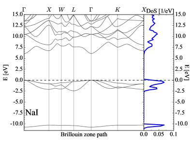
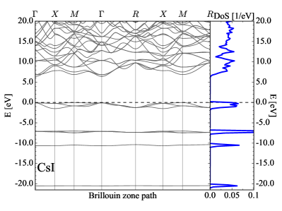
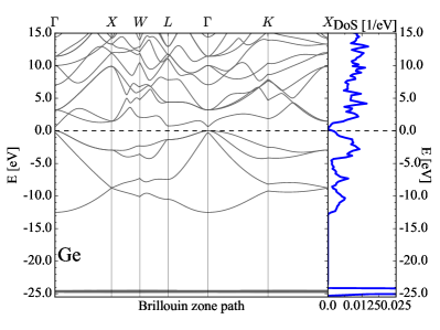
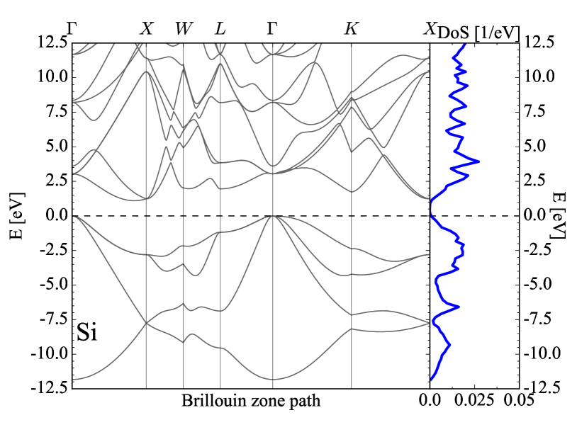
In these supplementary materials, we provide a few more details that are not essential for understanding the letter. In particular, we discuss the scintillation mechanisms of various materials mentioned in Table 1, as well as give a brief discussion on whether the effect of excitons should be included in the calculation of the DM-electron scattering rates. For completeness, we also provide plots showing our calculated band structures and density of states for the five elements shown in Fig. 2, as well as the recoil spectra for GaAs, NaI, and CsI.
X BRIEF REVIEW OF SCINTILLATION MECHANISMS
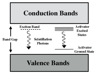
We review briefly the scintillation mechanisms of the materials listed in Table 1 of the letter. In general, for a material to be a scintillator, it must contain luminescent centers. These centers can be either extrinsic (e.g. dopants and impurities) or intrinsic (e.g. defects of the lattice or excitons), and give rise to a transition between a higher- and a lower-energy state. Moreover, the energy levels involved in the transition must be contained in a forbidden energy region (e.g. the band gap for semiconductors and insulators, or excimer states in gases) to avoid re-absorption of the emitted light or photoionization of the center (Fig. 3).
Pure CsI and NaI at cryogenic temperatures scintillate via the formation of self-trapped excitons, where an exciton (an electron-hole bound state) becomes self-trapped by deforming the lattice structure around it. At cryogenic temperatures the system lies at the minimum energy in lattice configuration space, and the system can only return to the ground state by emission of a photon. At higher temperatures, thermally induced lattice vibrations allow the system to return to the ground state by phonon emission resulting in a low radiative efficiency. At room temperature, this thermal quenching is over- come by doping the material with e.g. thallium. In these cases, Tl+ traps the excitons and provides an efficient luminescence center.
Direct-gap semiconductors, like GaAs, have the advantage that an excited electron can recombine with a hole without requiring a change in crystal momentum. In practice, however, dopants are used to enhance the radiative quantum efficiency, by providing radiative centers, and to reduce non-radiative recombination from impurities and native defects.
Indirect-gap semiconductors, like Si and Ge, require dopants to allow radiative recombination at cryogenic temperatures through the formation of a bound exciton that can radiate without the need for a change in crystal momentum.
Plastic scintillators consist of a base polymer that contains delocalized -orbital electrons and a small concentration of fluorescent molecules. Excited -orbital electrons will diffuse through the base polymer and excite fluorescent molecules. These excitations have radiative lifetimes of nanoseconds. This process is efficient both at room and cryogenic temperatures.
In tungstate scintillators, valence-band electrons on the oxygen ions can be excited to conduction band states on the tungsten ions. In PbWO4, the excited state is thermally quenched so that at room temperature the luminosity is low and the decay time is short. CaWO4 and CdWO4 are more efficient at room temperature and their decay times are 10 microseconds.
XI EFFECT OF EXCITONS ON DARK MATTER-ELECTRON SCATTERING-RATE CALCULATION
Our calculation of the DM-electron scattering rate neglects the effect of excitons. In this section, we discuss why we expect this to be a good approximation for the low-band-gap materials (Ge, Si, and GaAs), but that there may be an correction for the large-band-gap insulators (NaI and CsI).
Semiconductors or insulating crystals are characterized by a finite band gap, , between the top of the valence band and the bottom of the conduction band. These bands form an energy continuum for the excitation of an electron from the valence to the conduction band, which can be viewed as the creation of a free-electron-free-hole pair. In our calculation of the DM-electron scattering rate, we included the contribution of this continuum of states.
The small electrostatic Coulomb attraction between the negatively charged electron and positively charged hole creates an exciton, a bound electron-hole pair (see e.g. Knox (1963); Song and Williams (1996); Cho et al. (2012); Kubo and Hanamura (2012) and references therein). As we will see below, this Coulomb-bound electron-hole pair can be modeled with Rydberg-like states with energies , where is the binding energy and labels the Rydberg-like energy level. The energy of these excitons is therefore in the “forbidden” band-gap region, so that the density of states is nonzero even at energies slightly below the conduction band. Moreover, the bound electron-hole pair has ionized states with a continuous energy due to their relative motion. It turns out that excitons therefore also moderately increase the density of states just above the band gap compared to a calculation that neglects them. Including exciton effects in the DM-electron scattering-rate calculation could thus be important for two reasons. First, a nonzero density of states below the band gap means that the actual mass threshold is slightly lower. Second, any calculation that neglects exciton effects might underestimate slightly the scattering rate.
Excitons are extensively studied in solid state physics and play an important role in determining the properties of various materials. For example, it is well known that excitons are crucial in understanding the spectrum for the absorption of light, as they allow for photons with an energy just below to be absorbed by an electron. Similarly, excitons can play an essential role in determining the scintillation properties of a material. For example, an electron excited from the valence to the conduction band can quickly relax to the bottom of the conduction band and then into an exciton state by emitting phonons. The radiative decay of the exciton then yields a photon whose energy is just below that of the band gap. This typically allows the photon to traverse the material without being absorbed again, i.e. the material scintillates.
| [eV] | |||||
|---|---|---|---|---|---|
| CsI Alm ; Setyawan et al. (2009) | 5.65 | 0.312 | 2.270 | 0.117 | 2.37 |
| NaI Kamiyoshi and Nigara (1970); Setyawan et al. (2009) | 7.28 | 0.287 | 2.397 | 0.066 | 2.20 |
| GaAs Alm ; Singh (1992) | 12.85 | 0.067 | 0.45 | 0.005 | 20.3 |
| Ge Alm ; Singh (1992) | 16 | 0.2 | 0.28 | 0.006 | 12.7 |
| Si Alm ; Singh (1992) | 13 | 0.33 | 0.49 | 0.016 | 6.38 |
We can estimate how far below the conduction band the density of states will be nonzero from exciton effects by using a hydrogen-like model for the electron-hole pair. In particular, the exciton binding energies can be approximated by a modified Rydberg energy, namely
| (8) |
where is the dielectric constant of the crystal, , and is the effective electron-hole reduced mass, given by
| (9) |
where () is the effective electron (hole) mass. In this approximation, the electron-hole pair is assumed to be subject to a screened Coulomb potential characterized by the dielectric constant . This is a good approximation only if the exciton radius, , is much larger than the lattice constant (Wannier exciton). The exciton radius is given by
| (10) |
where is the (hydrogen) Bohr radius. The relevant values for the materials we considered in the letter are given in Table 3, which also lists the binding energy and size of the various 1s exciton states (i.e. with ).
The 1s-exciton radii listed in Table 3 for GaAs, Ge, and Si are much larger than the lattice constants given in Table 2, so that the approximation of the binding energies with Eq. (8) is expected to be reasonable. For NaI and CsI, the approximation is expected to be worse, but not dramatically so. We can thus use this simple estimate of the binding energies to reach at least qualitative conclusions for how the inclusion of exciton effects might affect the DM-mass threshold and the DM-electron scattering-rate calculation.
First, we see from Table 3 that the 1s-exciton binding energies for the low-band-gap materials, GaAs, Ge, and Si, are very small, meV, but even for the insulators, NaI and CsI, the binding energy only reaches about meV. This lowers the mass threshold by keV, depending on the material, an effect that is smaller than the numerical uncertainty of the rate calculation without excitons.
Second, recall that the electron’s recoil energy after a DM scattering event is typically several eV. The typical recoil energy is thus larger than the band gap energy for semiconductors like GaAs, Ge, and Si. A moderate increase in the density of states from the inclusion of exciton effects meV below the band gap, as well as just above it, is thus not expected to be important in the rate calculation. For the insulators NaI and CsI with band gaps around 6 eV, an increase in the density of states below and above the conduction band’s bottom could be somewhat important, since the electron will largely prefer to scatter to those states rather than higher-energy ones.
The calculation of exciton effects in the DM-electron scattering requires a dedicated effort. One reason for this is that existing numerical codes usually calculate exciton effects for photon absorption or emission. However, a photon being absorbed by an electron does not significantly change the momentum of the electron, so that the transition from valence to conduction band occurs at roughly the same -point. Instead, DM scattering off an electron does transfer a sizeable momentum, comparable with the crystal momentum.
The above discussion shows that it would be desirable to include exciton effects for NaI and CsI in the future. Neglecting the exciton effects, as we have done in our calculations, gives an overall conservative estimate for the DM-electron scattering rates.
XII RECOIL SPECTRA FOR GALLIUM ARSENIDE, SODIUM IODINE, AND CESIUM IODINE
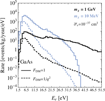
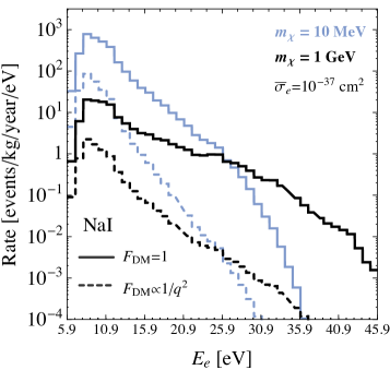
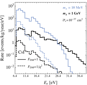
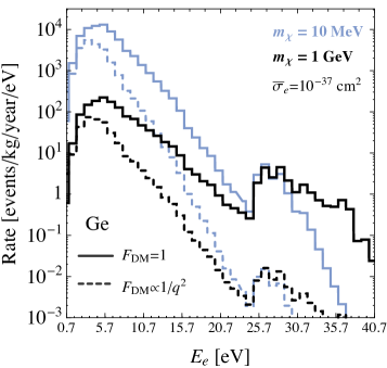
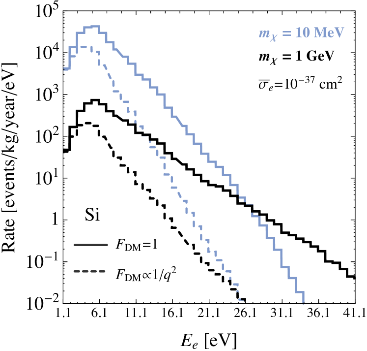
Fig. 4 shows the electron recoil spectra from DM-electron scattering for GaAs, NaI, and CsI. as a function of total deposited energy , for two DM masses and two choices for the DM form factor. We include also spectra for Ge and Si for comparison (see also Essig et al. (2016)). As expected, the spectra extend to higher recoil energies for higher DM masses, and spectra decrease faster than those for , since lower momentum transfers are preferred. Bump-like features in the spectra are explained by comparing the energy at which they occur with the energies of the available valence bands.
XIII DENSITY OF STATES AND BAND STRUCTURES
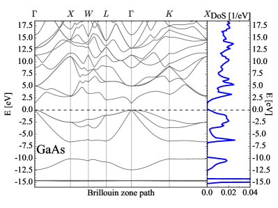
Fig. 5 shows our calculated band structure and density of states (DoS) for GaAs, NaI, and CsI. For completeness, we include slightly modified plots from Essig et al. (2016) for Ge and Si. We show all valence electron levels included in our DM-electron-scattering-rate calculation as well as the bottom of the conduction band.