Electrostatic control of quantum Hall ferromagnetic transition, a step toward reconfigurable network of helical channels
Abstract
Ferromagnetic transitions between quantum Hall states with different polarization at a fixed filling factor can be studied by varying the ratio of cyclotron and Zeeman energies in tilted magnetic field experiments. However, an ability to locally control such transitions at a fixed magnetic field would open a range of attractive applications, e.g. formation of a reconfigurable network of one-dimensional helical domain walls in a two-dimensional plane. Coupled to a superconductor, such domain walls can support non-Abelian excitation. In this article we report development of heterostructures where quantum Hall ferromagnetic (QHFm) transition can be controlled locally by electrostatic gating. A high mobility two-dimensional electron gas is formed in CdTe quantum wells with engineered placement of paramagnetic Mn impurities. Gate-induced electrostatic field shifts electron wavefunction in the growth direction and changes overlap between electrons in the quantum well and d-shell electrons on Mn, thus controlling the s-d exchange interaction and the field of the QHFm transition. The demonstrated shift of the QHFm transition at a filling factor is large enough to allow full control of spin polarization at a fixed magnetic field.
I Introduction
One of the key ingredient in the realization of topological superconductivityKitaev (2001) is to remove fermion doubling. The doubling is naturally absent in fully spin polarized systems, yet ferromagnetic spin arrangement is not compatible with a conventional s-wave superconductivity. It has been realized that spin doubling can be removed in spin-full systems if spin is locked to the carrier momentumFu and Kane (2008); Sau et al. (2010); Lutchyn et al. (2010); Oreg et al. (2010); Alicea (2010). While signatures of Majorana fermions have been reported in hybrid semiconductor/superconductor nanowires Rokhinson et al. (2012); Mourik et al. (2012); Churchill et al. (2013), removal of fermion doubling has been observed in electron transport only in the cleanest nanowires fabricated by cleaved edge overgrowth techniqueQuay et al. (2010).
An elegant proposal to circumvent fermion doubling is to couple two two-dimensional electron gases (2DEGs) with different sign of Landé -factor and subject then to a quantized magnetic fieldClarke et al. (2012); Stern and Lindner (2013). In a quantum Hall effect (QHE) regime two oppositely polarized counter-propagating edge channels at the boundary of two 2DEGs form a helical domain wall (h-DW), similar to helical channels at the edges of two-dimensional topological isolators Hasan and Kane (2010). Coupled to an s-wave superconductor, h-DW should support Majorana fermions in the integer QHE regime and parafermions in the fractional QHE regimeClarke et al. (2012).
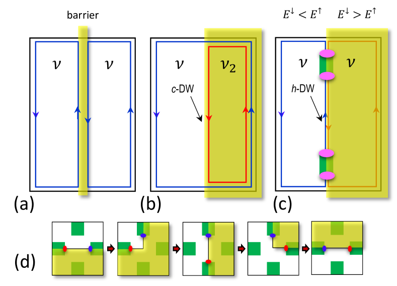
While bringing two different electron gases into a close proximity is an experimentally challenging proposition, we propose to use electrostatically controlled quantum Hall ferromagnetic (QHFm) transitions to form helical domain walls, see schematic in Fig. 1. In a QHE regime kinetic energy of electrons in a 2DEG is quantized into Landau levels (LL), which are further split due to the presence of spin. Polarization of a 2DEG and, more importantly, of the top filled energy level, depends on the number of occupied energy levels (the filling factor is a ratio of electron and magnetic flux densities), and changes as the system undergoes phase transitions between QHE states with different filling factors. If a 2D gas is separated into regions with different ’s by, e.g., electrostatic gating, chiral current-caring states are formed at the boundary. The actual order of spin-split energy levels is determined by an intricate balance between Zeeman, cyclotron and exchange energies. By shifting the balance it is possible to induce magnetic phase transitions between different QHE states with the same filling factor. QHFm transitions in integer and fractional QHE regimes have been studied extensively in the pastEisenstein et al. (1990); De Poortere (2000); Smet et al. (2001); Jaroszyński et al. (2002); Gusev et al. (2003); Betthausen et al. (2014). The QHFm transition field in those experiments was adjusted by in-plane (Zeeman) magnetic field , which does not afford local control of polarization.
In this article we report development and characterization of heterostructures where is sensitive to electrostatic gating, , and, thus, can be controlled locally, an enabling step toward experimental realization of theoretical concepts Clarke et al. (2012); Stern and Lindner (2013). In devices with multiple gates a possibility to reconfigure a network of h-DW opens a new class of systems where non-Abelian excitation can be created and manipulated.
II Electrostatic control of quantum Hall ferromagnet
II.1 QHFm transition in dilute magnetic semiconductor
Electrostatic control of QHFm transitions is realized in a dilute magnetic semiconductor CdTe:Mn with engineered placement of paramagnetic impurities. Substitutional Mn is a neutral impurity in CdTe and fractional QHE has been observed in high mobility CdTe:Mn two-dimensional electron gases with of MnBetthausen et al. (2014). Exchange interaction between d-electrons on Mn (spin ) and s-electrons in the QW modifies energy spectrum of a 2DEG and results in unusual spin splitting and level crossing at high magnetic fieldsWojtowicz et al. (1999). QHFm transition in both integer and fractional QHE regimes have been observed in tilted magnetic fields experiments in QWs with uniform Mn doping Jaroszyński et al. (2002); Betthausen et al. (2014). In the presence of magnetic field spin-dependent energy in dilute magnetic semiconductors is Furdyna (1988):
| (1) |
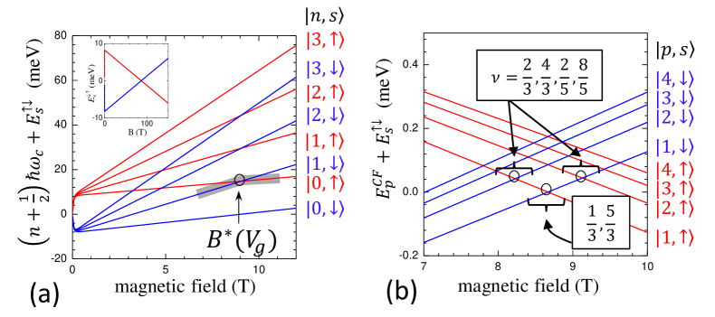
where the first term is the Zeeman splitting and the second term is due to an s-d exchange. Here in CdTe, meV Gaj et al. (1994); Kiselev et al. (1998), is an effective Mn concentration, and is due to Mn-Mn antiferromagnetic interaction. At low fields spin splitting is dominated by a large positive exchange term, while at high fields and low temperatures the Brillouin function and -dependence is dominated by the negative Zeeman term. In Fig. 2 we plot spin splitting of energy levels (1) and spectrum of Landau levels (LL) for electrons and composite fermions (CF) , where energy gaps between CF levelsPark and Jain (1998) . Here is the reduced Plank’s constant, is the cyclotron frequency, is the charging energy, is the magnetic length, constant depends on the confining potential Liu et al. (2014), and . The field of spin subbands crossing for the same LL ( and ) or neighboring LLs ( and ) depends on the strength of the s-d exchange interaction . Thus, engineering heterostructures with gate-tunable s-d exchange will allow local control of spin polarization in both integer and fractional QHE regimes.
II.2 Heterostructures with s-d exchange control
The second term in (1) is a mean-field approximation to the exchange Hamiltonian , where interaction of an electron at a position with a large number of Mn ions at positions is approximated as an overlap of the electron wavefunction with a uniform Mn background within and an average magnetization . For quantum wells with homogeneous Mn distribution throughout the whole QW region an integral has weak dependence on the shape of and level crossing field is almost independent of a gate voltage Jaroszyński et al. (2002).
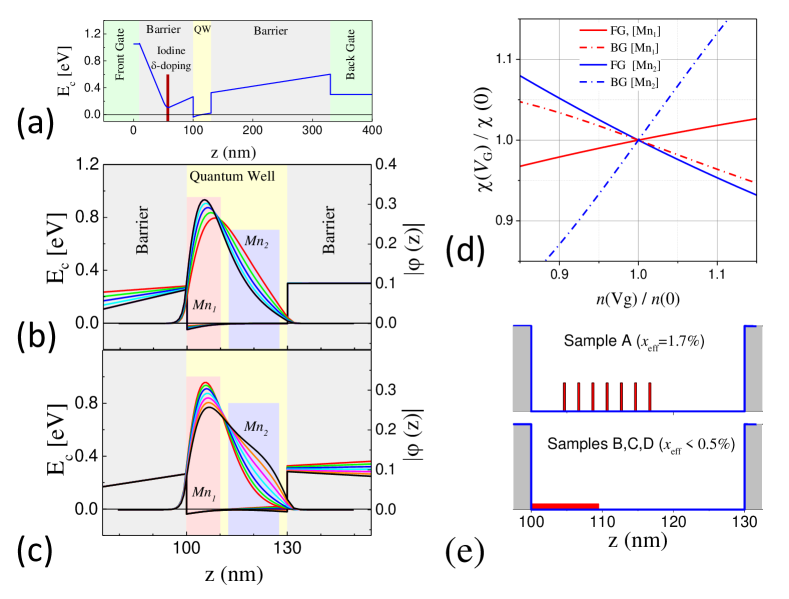
We now consider non-uniform distribution of Mn inside a QW, e.g. Mn is confined to regions or within the QW, see Fig. 3b,c. In these regions has strong dependence on the out-of-plane electric field and becomes gate dependent, . Application of positive (negative) voltage to the front gate shifts electron wavefunction closer to (away from) the surface, for and for . Gate voltage also changes electron density , thus for and for for the front gate. Application of a back gate voltage results in a density change but electrical field shifts wavefunction in the opposite direction, thus for and for for the back gate. Described behaviour is summarized on a Fig.3d. For the formation of well defined h-DWs we want to control with a minimal change of in order to remain at the same filling factor , or maximize .
In order to demonstrate electrostatic control of QHFm transition several Cd1-xMnxTe/ Cd0.8Mg0.2Te quantum well heterostructures were grown by molecular beam epitaxy (MBE), see Jaroszyński et al. (2002); Betthausen et al. (2014) for details. Iodine delta-doping layer is separated from the QW by a 30 nm Cd0.8Mg0.2Te spacer. Mn was introduced into the QW region either as a digital -doping or as a continuous doping, see schematics in Fig. 3e. More than 35 wafers have been grown and characterized with different Mn placement and concentration, here we report data on 4 representative wafers with , 0.34%, 0.20% and 0.085% (wafers A,B,C and D). Samples were patterned into m-wide Hall bars. A semitransparent Ti front gate (10 nm thick) was thermally evaporated onto the central part of Hall bars. Ohmic contacts were produced by soldering freshly cut indium ingots similar to previous studies Jaroszyński et al. (2002); Betthausen et al. (2014). Copper foil glued to the back of samples served as a back gate. Devices were illuminated with a red LED at 4 K, low temperature electron density and mobility were in the range of cm-2 and cm2/Vs in different samples. Electron transport was measured in a dilution refrigerator using standard ac technique with 10 nA excitation.
II.3 Smooth QHFm transition at
Spin levels crossing measured in optical experimentsWojtowicz et al. (1999) and QHFm transitions observed in the fractional QHE regimeBetthausen et al. (2014) are well described by Eq. 1 and the values of extracted from the beating of Shubnikov - de Haas (SdH) oscillations at low fieldsTeran et al. (2002). Yet, we did not observe any re-entrant behavior at . We conclude that the absence of a transport signature of the QHFm transition at is either due to a phase separation in the vicinity of the transition or strong e-e exchange interaction and anticrossing of levels with the same orbital wavefunction.
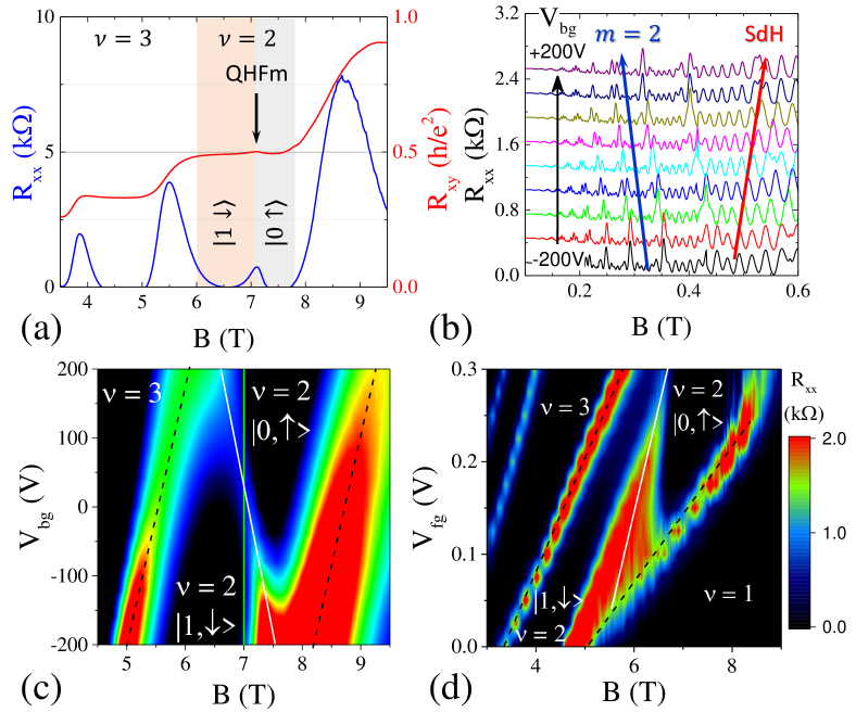
An ability to locally control exchange interaction for small is crucial for the formation of h-DW in a fractional quantum Hall regime, a prerequisite for the creation of higher order non-Abelian excitations. The strength of the exchange interaction can be obtained from the beating in the SdH regime, where the -th node is defined by the condition Teran et al. (2002) . Gate dependence of magnetoresistance in wafer C at low fields is shown in Fig. 4b. Nodes are shifted to lower fields as the voltage on the back gate increases, . At the same time SdH peaks shift to higher fields, , and as is expected for the [Mn1] doping arrangement.
II.4 Gate control of sharp QHFm transition at
Unlike QHFm transition at , the transition at involves states from different Landau levels and e-e exchange is strongly suppressed. Also, at level crossing has much stronger -dependence meV/T, as compared to meV/T at , which suppresses phase separation. As a result quantization is lifted in the vicinity of the QHFm transition and a prominent signature in magnetoresistance is observedJaroszyński et al. (2002).
Magnetoresistance in sample A is shown in Fig. 4a. A small peak at Tesla in the middle of the state is the QHFm phase transition between and states, polarization of the top filled energy level changes across the transition. In the color plots magnetoresistance is plotted as a function of voltage on the front and back gates (Fig. 4c,d), measurements are performed by sweeping magnetic field at constant gate voltages. Electron density increases with the increase of and and peaks between adjacent QHE states shift to higher in both plots. In contrast, the QHFm transition shifts in opposite directions as a function of and , consistent with the modelling of the wavefunction-Mn1 overlap in Fig. 3d. Note that for Tesla polarization of the top level can be tuned between and states by electrostatic gating, thus realizing the theoretical concept of Fig. 2a.
Gate control of the s-d exchange is summarized in Fig. 5a for several wafers. The absolute values of Mn concentration and s-d overlap cannot be measured independently with high accuracy, by a relative change of the exchange interaction can be obtained from the gate dependence of the experimentally measured . Slopes are in a good agreement with obtained from band simulations, Fig. 3d. Note that the efficiency of the s-d exchange control depends on the slope: for QHFm transitions in the integer QHE regime and in the fractional QHE regime for large fields.
II.5 Spin-orbit-induced gap for QHFm transition
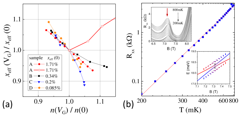
The height of the peak at has exponential -dependence and vanishes at low temperatures with an activation energy , see Fig. 5b. We attribute this small gap to the level anticrossing due to the spin-orbit (SO) coupling between neighboring LLs. Energy spectrum in the presence of SO interactions is calculated by adding Dresselhaus and Rashba spin-orbit terms to the single-particle Hamiltonian of a 2D gas in magnetic field in the presence of s-d coupling (1), square well confinement potential in direction, and electric field potential , see Appendix for details. Here and are the Dresselhaus and Rashba constants, and is defined as . The energy spectrum near and levels crossing is plotted in the insert in Fig. 5b. The value of the anticrossing gap is found to depend only on the Rashba spin-orbit coupling
| (2) |
For an average electric field of , and the calculated gap eV, in a good agreement with the experimentally measured activation gap of 96 eV. We note that an ability to open a topologically trivial (spin-orbit) gap is required for the localization of non-Abelian excitations Clarke et al. (2012).
III Conclusions
In this paper we propose a new experimentally feasible platform to realize non-Abelian excitations. The platform is based on the ability to create ferromagnetic domains in a quantum Hall effect regime, where helical domain walls are formed at the domain boundaries. These domain walls, coupled to a superconductor with high critical field , should support Majorana and higher order non-Abelian excitations. Topological protection of the QHE regime insures that only single channel with removed fermion doubling is formed, thus alleviating multi-channel complication encountered in nanowire-based devices. As a proof-of-concept we developed CdTe quantum well heterostructures with engineered placement of paramagnetic Mn impurities and demonstrated local control of the QHFm transition at by electrostatic gating. Further research is needed to develop superconducting contacts to CdTe, a possible path is to overgrow CdTe with HgCdTe/HgTe epilayers where ohmic contacts with a high- superconductor Nb have been demonstratedOostinga et al. (2013).
IV Acknowledgements
Authors acknowledge support by the U.S. Department of Energy, Office of Basic Energy Sciences, Division of Materials Sciences and Engineering under Awards DE-SC0008630 (A.K and L.P.R.), by the Department of Defence Office of Naval research Award N000141410339 (A.K, T.W., G.S. and Y. L-G.), by the National Science Centre (Poland) grant DEC-2012/06/A/ST3/00247 (V.K., Z.A., G.K., and T.W.), and by the Foundation for Polish Science (T.W.).
*
Appendix A Calculation of spin-orbit–induced anticrossing of LLs in the presence of s-d exchange
A general single-particle Hamiltonian can be written as:
where is a vector containing Pauli matrices, is an electric potential, and is a confinement potential in direction, the fifth term is s-d exchange with Mn impurities and the last two terms are Dresselhaus and Rashba spin-orbit coupling. is defined as , where and . Magnetic field corresponds to a vector potential .
For exchange interaction we use a mean-field model described in the main text , where is the density of ions, is the Brillouin function, is Boltzmann’s constant, and is a unit vector in the direction of magnetic field. We consider high-field limit . We also assume uniform Mn doping in the range . Electric potential is , we consider .
The Hamiltonian describing motion in direction is
| (4) |
Its eigenvalues for the lowest subband are:
where is the Airy function, is its first zero, , and for spin up states and for spin down.
In the presence of perpendicular magnetic field an effective Hamiltonian is
| (6) |
where lowering and rising operators are defined as , , is the magnetic length, and is the cyclotron energy.
We treat spin-orbit couplings as perturbations and found that only Rashba term has a non-zero matrix element between and energy levels. In the vicinity of crossing the energy spectrum is
| (7) |
and the anticrossing gap is given by Eq. 2.
References
- Kitaev (2001) A Yu Kitaev, “Unpaired Majorana fermions in quantum wires,” Physics-Uspekhi 44, 131 – 136 (2001).
- Fu and Kane (2008) Liang Fu and C.L. Kane, “Superconducting proximity effect and Majorana fermions at the surface of a topological insulator,” Physical Review Letters 100, 096407 (2008).
- Sau et al. (2010) Jay D. Sau, Sumanta Tewari, and S. Das Sarma, “Universal quantum computation on a semiconductor quantum wire network,” Phys. Rev. A 82,, 052322 (2010), 1007.4204 .
- Lutchyn et al. (2010) Roman M. Lutchyn, Jay D. Sau, and S. Das Sarma, “Majorana fermions and a topological phase transition in semiconductor-superconductor heterostructures,” Phys. Rev. Lett. 105, 077001 (2010).
- Oreg et al. (2010) Yuval Oreg, Gil Refael, and Felix von Oppen, “Helical liquids and Majorana bound states in quantum wires,” Phys. Rev. Lett. 105, 177002 (2010).
- Alicea (2010) Jason Alicea, “Majorana fermions in a tunable semiconductor device,” Phys. Rev. B 81, 125318 (2010).
- Rokhinson et al. (2012) Leonid P. Rokhinson, Xinyu Liu, and Jacek K. Furdyna, “The fractional a.c. Josephson effect in a semiconductor-superconductor nanowire as a signature of Majorana particles,” Nat. Phys. 8, 795 – 799 (2012).
- Mourik et al. (2012) V. Mourik, K. Zuo, S. M. Frolov, S. R. Plissard, E. P. A. M. Bakkers, and L. P. Kouwenhoven, “Signatures of Majorana fermions in hybrid superconductor-semiconductor nanowire devices,” Science 336, 1003 – 1007 (2012).
- Churchill et al. (2013) H. O. H. Churchill, V. Fatemi, K. Grove-Rasmussen, M. T. Deng, P. Caroff, H. Q. Xu, and C. M. Marcus, “Superconductor-nanowire devices from tunneling to the multichannel regime: Zero-bias oscillations and magnetoconductance crossover,” Phys. Rev. B 87, 241401 (2013).
- Quay et al. (2010) C.H.L. Quay, T.L. Hughes, J.A. Sulpizio, L.N. Pfeiffer, K.W. Baldwin, K.W. West, D. Goldhaber-Gordon, and R. de Picciotto, “Observation of a one-dimensional spin-orbit gap in a quantum wire,” Nature Physics 6, 336 – 339 (2010).
- Clarke et al. (2012) David J. Clarke, Jason Alicea, and Kirill Shtengel, “Exotic non-Abelian anyons from conventional fractional quantum Hall states,” Nat. Commun. 4, 1348 (2012).
- Stern and Lindner (2013) Ady Stern and Netanel H. Lindner, “Topological quantum computation - from basic concepts to first experiments,” Science 339, 1179 – 1184 (2013).
- Hasan and Kane (2010) M. Z. Hasan and C. L. Kane, “Topological insulators,” Rev. Mod. Phys. 82, 3045–3067 (2010).
- Eisenstein et al. (1990) J. P. Eisenstein, H. L. Stormer, L. N. Pfeiffer, and K. W. West, “Evidence for a spin transition in the fractional quantum Hall effect,” Phys. Rev. B 41, 7910–7913 (1990).
- De Poortere (2000) E. P. De Poortere, “Resistance spikes at transitions between quantum Hall ferromagnets,” Science 290, 1546–1549 (2000).
- Smet et al. (2001) J. H. Smet, R. A. Deutschmann, W. Wegscheider, G. Abstreiter, and K. von Klitzing, “Ising ferromagnetism and domain morphology in the fractional quantum Hall regime,” Phys. Rev. Lett. 86, 2412–2415 (2001).
- Jaroszyński et al. (2002) J. Jaroszyński, T. Andrearczyk, G. Karczewski, J. Wróbel, T. Wojtowicz, E. Papis, E. Kamińska, A. Piotrowska, Dragana Popović, and T. Dietl, “Ising quantum Hall ferromagnet in magnetically doped quantum wells,” Phys. Rev. Lett. 89, 266802 (2002).
- Gusev et al. (2003) G.M. Gusev, A.A. Quivy, T.E. Lamas, J.R. Leite, O. Estibals, and J.C. Portal, “Quantum Hall ferromagnet in a parabolic well,” Physical Review B 67, 155313 (2003).
- Betthausen et al. (2014) C. Betthausen, P. Giudici, A. Iankilevitch, C. Preis, V. Kolkovsky, M. Wiater, G. Karczewski, B. A. Piot, J. Kunc, M. Potemski, T. Wojtowicz, and D. Weiss, “Fractional quantum Hall effect in a dilute magnetic semiconductor,” Phys. Rev. B 90, 115302 (2014).
- Wojtowicz et al. (1999) T. Wojtowicz, M. Kutrowski, G. Karczewski, J. Kossut, F. J. Teran, and M. Potemski, “-factor dependence of the evolution of magneto-optical spectra with the density of quasi-two-dimensional electrons in heterostructures,” Phys. Rev. B 59, R10437–R10440 (1999).
- Furdyna (1988) J.K. Furdyna, “Diluted magnetic semiconductors,” Journal of Applied Physics 64, R29 (1988).
- Gaj et al. (1994) J. Gaj, W. Grieshaber, C. Bodin-Deshayes, J. Cibert, G. Feuillet, Y. Merle d’Aubigné, and A. Wasiela, “Magneto-optical study of interface mixing in the CdTe-(Cd,Mn)Te system,” Physical Review B 50, 5512–5527 (1994).
- Kiselev et al. (1998) A.A. Kiselev, E.L. Ivchenko, A.A. Sirenko, T. Ruf, M. Cardona, D.R. Yakovlev, W. Ossau, A. Waag, and G. Landwehr, “Electron and hole g factor anisotropy in CdTe/CdMgTe quantum wells,” Journal of Crystal Growth 184-185, 831–834 (1998).
- Park and Jain (1998) K. Park and J. K. Jain, “Phase diagram of the spin polarization of composite fermions and a new effective mass,” Phys. Rev. Lett. 80, 4237–4240 (1998).
- Liu et al. (2014) Yang Liu, S. Hasdemir, A. Wójs, J. K. Jain, L. N. Pfeiffer, K. W. West, K. W. Baldwin, and M. Shayegan, “Spin-polarization of composite fermions and particle-hole symmetry breaking,” Physical Review B 90,, 085301 (2014), arXiv:1406.2387 .
- (26) “nextnano3 nanodevice simulator,” http://www.nextnano.de/nextnano3/.
- Teran et al. (2002) F. Teran, M. Potemski, D. Maude, T. Andrearczyk, J. Jaroszynski, and G. Karczewski, “Pauli paramagnetism and Landau level crossing in a modulation doped CdMnTe/CdMgTe quantum well,” Physical Review Letters 88, 186803 (2002).
- Oostinga et al. (2013) Jeroen B. Oostinga, Luis Maier, Peter Schüffelgen, Daniel Knott, Christopher Ames, Christoph Brüne, Grigory Tkachov, Hartmut Buhmann, and Laurens W. Molenkamp, “Josephson supercurrent through the topological surface states of strained bulk HgTe,” Phys. Rev. X 3, 021007 (2013).