Origin of the Metal-Insulator Transition of Indium Atom Wires on Si(111)
Abstract
As a prototypical one-dimensional electron system, self-assembled indium (In) nanowires on the Si(111) surface have been believed to drive a metal-insulator transition by a charge-density-wave (CDW) formation due to electron-phonon coupling. Here, our first-principles calculations demonstrate that the structural phase transition from the high-temperature 41 phase to the low-temperature 82 phase occurs through an exothermic reaction with the consecutive bond-breaking and bond-making processes, giving rise to an energy barrier between the two phases as well as a gap opening. This atomistic picture for the phase transition not only identifies its first-order nature but also solves a long-standing puzzle of the origin of the metal-insulator transition in terms of the 2 periodic lattice reconstruction of In hexagons via bond breakage and new bond formation, not by the Peierls instability-driven CDW formation.
pacs:
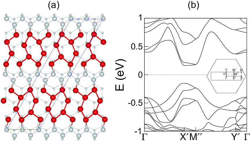
73.20.At, 68.35.Md, 71.30.+hLow-dimensional electronic systems are of great interest in contemporary condensed-matter physics because of their susceptibility to charge density wave (CDW) instability Carpinelli , non-Fermi liquid behavior Blumenstein , spin ordering Erwin ; Li , and superconductivity Qin ; TZhang at low temperatures. Specifically, metal-atom adsorption on semiconductor surfaces provides a unique playground for the exploration of such exotic physical phenomena Tejeda ; Snijders . We here focus on a prototypical example of quasi-one-dimensional (1D) systems, self-assembled indium (In) atom wires on the Si(111) surface Bunk ; Yeom1 ; Cho . Each In wire consists of two zigzag chains of In atoms [see the left panel of Fig. 1(a)] Bunk . Below 120 K, this quasi-1D system undergoes a reversible phase transition initially from a 41 structure to a 42 one, then to an 82 structure Yeom1 ; Kumpf , showing a period doubling both parallel and perpendicular to the In wires. This (41)(82) structural phase transition is accompanied by a metal-insulator (MI) transition Yeom1 ; Ahn ; Yeom2 . For the explanation of such a MI transition, the CDW mechanism due to a Peierls instability was initially proposed Yeom1 ; Ahn ; Yeom2 ; Park , but subsequently other mechanisms based on an order-disorder transition Gonzalez1 ; Gonzalez2 and many-body interactions GLee have been proposed. Despite such debates, the CDW mechanism has been most widely believed to drive the observed MI transition Yeom1 ; Ahn ; Yeom2 ; Park ; Morikawa ; SHUhm ; DMOh . It is noted that the CDW formation invokes the strong coupling between lattice vibrations and electrons near the Fermi level , caused by Fermi surface nesting with a nesting vector 2 = / (: the 41 lattice constant along the In wires) Yeom1 ; Gruner . The resulting Peierls dimerization was believed to occur on each chain, and the two dimerized chains further interact with each other, leading to a coupled double Peierls-dimerized chain model Cheon [see Fig. 1(b)].
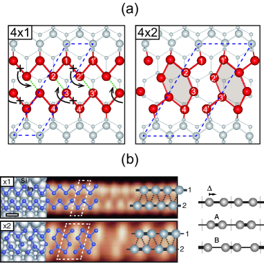
Regarding the phase transition of the In/Si(111) system, there are still some unsettled issues. Although it is well established that the structural model of the 82 phase is constituted by the basic building block of In “hexagon” [see the right panel of Fig. 1(a)], the microscopic mechanism of the hexagon formation is so far unclear whether it is driven by the Peierls dimerization on the two chains Yeom1 ; Cheon or by a shear distortion where neighboring chains are displaced in opposite directions Gonzalez1 . Recently, it was also reported that both the covalent bonding and van der Waals (vdW) interactions between the two chains play crucial roles in forming In hexagons HJKim . Moreover, the order of the phase transition has been controversial whether it belongs to first-order Park2 ; Wall ; Klasing or second-order Gonzalez1 ; Gonzalez2 ; Guo ; GLee2 . According to the mean-field theory Gruner , the CDW or order-disorder mechanism can be classified as the second-order phase transition. However, existing scanning tunneling microscopy (STM) experiments have reached the conflicting conclusions between the first-order Park2 and second-order Guo ; GLee2 transitions, whereas a recent high-resolution low-energy electron diffraction (HRLEED) study Klasing observed a robust hysteresis of diffraction spot intensities as the sample temperature slowly increases and decreases during the (41)(82) phase transition. The latter observation Klasing obviously indicates the existence of energy barrier between the two phases, representing the first-order transition Landau . All of these controversies on the microscopic mechanism of the hexagon formation and the order of the phase transition reflect our incomplete understanding of the origin of the phase transition in the In/Si(111) system.
In this paper, using first-principles density-functional theory (DFT) calculations, we propose the atomistic picture for the phase transition of the In/Si(111) system to resolve the existing problems such as the microscopic mechanism of the hexagon formation, the order of the phase transition, as well as the origin of the MI transition. We find that the hexagon formation is driven by an exothermic reaction with the consecutive bond-breaking and bond-making processes, giving rise to an energy barrier as well as a gap opening. This atomistic picture not only reveals the first-order nature of the (41)(82) phase transition, but also illustrates how the observed solitons Zhang ; THKim ; Cheon can be created at the boundary of two differently oriented hexagon structures. Our findings clarify that the MI transition of the In/Si(111) system is attributed to the 2 periodic lattice reconstruction of In hexagons via the bond breakage and the new bond formation, rather than the CDW formation arising from Fermi surface nesting Yeom1 ; Ahn ; Yeom2 ; Park ; Cheon .
To properly predict the energetics of the 41, 42, and 82 structures HJKim ; Zhang2 ; SWKim , we have performed the van der Waals energy corrected vdW hybrid DFT calculations using the FHI-aims Aims code that gives an accurate, all-electron description based on numeric atom-centered orbitals, with “tight” computational settings. For the exchange-correlation energy, we employed the hybrid functional of HSE06 HSE1 ; HSE2 . The -space integrations in various unit-cell calculations were done equivalently with 64 points in the surface Brillouin zone of the 41 unit cell. The Si(111) substrate (with the Si lattice constant = 5.418 Å) below the In chains was modeled by a 6-layer slab with 30 Å of vacuum in between the slabs. Each Si atom in the bottom layer was passivated by one H atom. All atoms except the bottom layer were allowed to relax along the calculated forces until all the residual force components were less than 0.01 eV/Å.
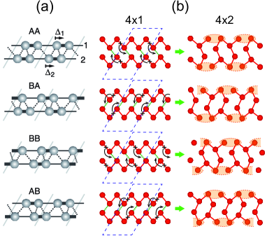
According to the previously proposed CDW mechanism Yeom1 ; Ahn ; Yeom2 ; Park ; Cheon of the structural phase transition, the ground state of the In wire was described by a double Peierls-dimerized chain model with a zigzag interchain coupling between two chains [see Fig. 1(b)]: that is, below 120 K, the In wire undergoes a period doubling CDW transition through the Peierls dimerization on both chains. Since there are the two dimerization directions that form “A” phase with a positive displacement and “B” phase with a negative [see Fig. 1(b)] on the two chains [i.e., chain “1” and chain “2” in Fig. 1(b)], the double chain can have four degenerate CDW ground phases, which were denoted as AA, BA, BB, and AB in Ref. Cheon [see Fig. 2(a)]. It is, however, noticeable that such a coupled double Peierls-dimerized atomic chain is unlikely to be fit well for the well-established hexagon structural model Gonzalez1 which involves the bond formation between the two chains. Therefore, we here propose a new atomistic model of the hexagon formation, where the bonds on the chains 1 and 2 are broken to form the new bonds between both chains. For one example of such bond breakage and new bond formation, the bond between In1 and In atoms on chain 1 and the bond between In3 and In atoms on chain 2 are broken to form the new bonds and , respectively, leading to the formation of the 42 hexagon structure [see Fig. 1(a)]. Note that the bond breaking/forming of / accompanies that of / and vice versa, as discussed below. Since there are four different bonds on chain 1 (or 2) within the 42 unit cell, four degenerate hexagon structures can be generated as shown in Fig. 2(b), which correspond to AA, BA, BB, and AB configurations in Ref. Cheon .
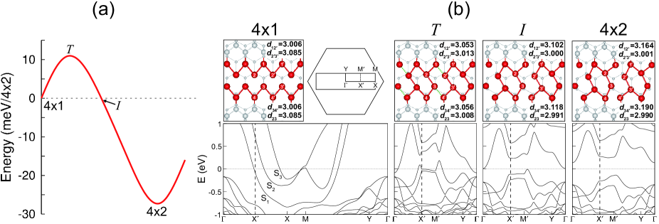
The present atomistic model of the hexagon formation is expected to have an energy barrier for the consecutive bond-breaking and bond-making processes. To find this energy barrier, we calculate the energy profile along the transition path between the 41 and 42 structures by using the nudged elastic-band method NEB . The calculated energy profile is displayed in Fig. 3(a). We find that the transition () state is higher in energy than the 41 structure by 5.4 meV per 41 unit cell, yielding an energy barrier () of 11 meV on going from the 41 to the 42 structure. Since the 42 structure is more stable than the 41 structure by 13.6 meV per 41 unit cell (see Table I), we can say that the hexagon formation occurs through an exothermic reaction with bond breakage and new bond formation. It is noted that the 82 structure is further stabilized over the 41 structure by 32.9 meV per 41 unit cell (see Table I), and is reduced to be 8 meV on going from 41 to 82, which is much smaller than that ( = 40 meV) obtained by a previous DFT calculation with the local-density approximation Wall . The existence of the energy barrier for the (41)(82) phase transition is consistent with a recent HRLEED experiment Klasing where the energy barrier was confirmed by the observation of a hysteresis of diffraction spot intensities upon slow increase and decrease of the sample temperature at the (41)(82) phase transition. Thus, the present theory and the previous HRLEED experiment support the first-order nature of the phase transition, contrasting with the second-order nature deduced from the CDW Guo ; GLee2 or order-disorder mechanism Gonzalez1 ; Gonzalez2 .
Figure 3(b) shows the atomic geometries of the state and an intermediate () state, together with those of the 41 and 42 structures. We find that, along the transition path from the 41 to the 42 phase, the In-In interatic distance () increases as 3.01 (3.01), 3.05 (3.06), 3.10 (3.12), and 3.16 (3.19) Å for 41, , , and 42, respectively, while () decreases as 3.09 (3.09), 3.01 (3.01), 3.00 (2.99), and 3.00 (2.99) Å [see Fig. 3(b)]. These results indicate that during the structural phase transition the bond breakage of proceeds the new bond formation of , simultaneously taking place with the bond breakage of and the new bond formation of . It is noticeable that such bond-breaking and bond-making processes leading to the hexagon formation were not taken into account in the coupled double Peierls-dimerized chain model Cheon . Thus, unlike the present atomistic model of the hexagon formation, the latter model Cheon does not properly describe the hexagon structure of the indium wire.
| 42 | 82 | |
|---|---|---|
| (meV per 41 unit cell) | –13.6 | –32.9 |
| (eV) | 0.27 | 0.31 |
The calculated surface band structures along the transition path between the 41 and 42 structures are also displayed in Fig. 3(b). We find that the 41 structure has the three surface bands , , and crossing the Fermi level, showing a metallic feature. On the other hand, it is clearly seen that the band gap opens during the bond-breaking and bond-making processes. Specifically, the gap opening starts from the state, leading to a band gap () of 0.27 (0.31) eV at the 42 (82) structure: see Fig. 3(b) (Fig. 5S of the Supplemental material supp ). These values of agree well with those (0.3 eV) obtained from surface transport measurements Tanikawa and scanning tunneling spectroscopy Gonzalez2 . Based on a coupled double Peierls-dimerized chain model [see Fig. 1(b)], a tight-binding Hamiltonian analysis showed that the Peierls dimerization on both chains hybridizes the and states to produce a gap opening Cheon . However, this Peierls instability-driven gap opening is characteristically different from the present gap opening driven by the 2 periodic lattice reconstruction of In hexagons that involves the bond-breaking and bond-making processes within the In wire. Since the former Peierls chain model Cheon is lacking in the atomic description of the hexagon structure as discussed above, we believe that the CDW mechanism would not be the origin of the MI transition of the In/Si(111) system.
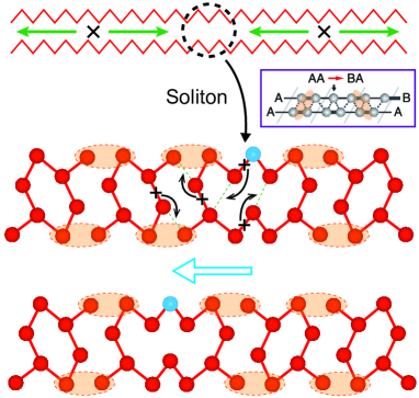
Finally, it is noteworthy that the coupled double Peierls chain model classified three types of topological edge states at the domain boundary between two different CDW phases Cheon : i.e., right-chiral, left-chiral, and nonchiral solitons among the total twelve possible solitons arising from four degenerate CDW phases. However, there remain the question of how the multiple CDW phases and the resulting solitons can be created from the 41 phase along the In wires. Based on the present atomistic picture for the phase transition, we speculate that around the phase transition temperature the bond breakage takes place at random sites of the 41 phase, initiating the hexagon formation which then propagates along the In wire (see sketch in the upper panel of Fig. 4). This speculation is supported by our calculation with a larger 48 supercell, where after the formation of a single hexagon it is converged to the 42 hexagon structure without any barrier. Indeed, the propagation of the hexagon structure was observed by an ultrafast time-resolved reflection high energy electron diffraction experiment Wall where adsorbates trigger the propagation of the phase front of the 82 structure with a constant velocity of 82 m/s. Therefore, a soliton is expected to be created at the midpoint between two bond-breakage positions after the propagation of two different hexagon structures [see Fig. 2(b)] in the opposite directions. Moreover, the created solitons can move along the In wire by the activation of bond-breaking and bond-making processes. For instance, one soliton structure corresponding to the AABA configuration in Ref. Cheon is sketched in Fig. 4, together with its movement. Future theoretical and experimental works are anticipated to investigate the detailed kinetics of solitons such as the activation energy for the soliton motion, the propagation speed of solitons, the transformation of soliton configurations, and so on.
In summary, based on first-principles DFT calculations, we have proposed the atomistic picture for the phase transition of the In/Si(111) system, where the low-temperature hexagon structure is formed through an exothermic reaction with the consecutive bond-breaking and bond-making processes. During such bond breakage and new bond formation, we found the existence of an energy barrier as well as a gap opening. Therefore, we revealed not only the first-order nature of the (41)(82) phase transition but also the origin of the MI transition in terms of the 2 periodic lattice reconstruction of In hexagon, rather than the prevailing Peierls instability-driven CDW mechanism. We anticipate that our findings will stimulate future theoretical and experimental works to reinterpret many of the existing controversial issues in the prototypical 1D In/Si(111) system in the light of the presently proposed atomistic picture for the phase transition.
This work was supported by National Research Foundation of Korea (NRF) grant funded by the Korea Government (MSIP) (2015R1A2A2A01003248). The calculations were performed by KISTI supercomputing center through the strategic support program (KSC-2015-C3-044) for the supercomputing application research. S.W.K. acknowledges support from POSCO TJ Park Foundation.
∗ Corresponding author: chojh@hanyang.ac.kr
References
- (1) J. M. Carpinelli, H. H. Weitering, E.W. Plummer, and R. Stumpf, Nature (London) 381, 398 (1996).
- (2) C. Blumenstein, J. Schäfer, S. Mietke, S. Meyer, A. Dollinger, M. Lochner, X. Y. Cui, L. Patthey, R. Matzdorf, and R. Claessen, Nat. Phys. 7, 776 (2011).
- (3) S. C. Erwin and F. J. Himpsel, Nat. Commun. 1, 58 (2010).
- (4) G. Li, P. Hopfner, J. Schafer, C. Blumenstein, S. Meyer, A. Bostwick, E. Rotenberg, R. Claessen, and W. Hanke, Nat. Commun. 4, 1620 (2013).
- (5) S. Qin, J. Kim, Q. Niu, and C. K. Shih, Science 324, 1314 (2009).
- (6) T. Zhang, P. Cheng, W.-J. Li, Y.-J. Sun, G. Wang, X.-G. Zhu, K. He, L. Wang, X. Ma, X. Chen, Y. Wang, Y. Liu, H.-Q. Lin, J.-F. Jia, and Q.-K. Xue, Nat. Phys. 6, 104 (2010).
- (7) P. Snijders and H. Weitering, Phys. Mod. Phys. 82, 307 (2010), and references therein.
- (8) A. Tejeda, Y. Fagot-Révurat, R. Cortés, D. Malterre, E. G. Miche, and A. Mascaraque, Phys. Status Solidi A 209, 614 (2012), and references therein.
- (9) H. W. Yeom, S. Takeda, E. Rotenberg, I. Matsuda, K. Horikoshi, J. Schaefer, C. M. Lee, S. D. Kevan, T. Ohta, T. Nagao, and S. Hasegawa, Phys. Rev. Lett. 82, 4898 (1999).
- (10) O. Bunk, G. Falkenberg, J. H. Zeysing, L. Lottermoser, R. L. Johnson, M. Nielsen, F. Berg-Rasmussen, J. Baker, and R. Feidenhans’l, Phys. Rev. B 59, 12228 (1999).
- (11) J.-H. Cho, D. H. Oh, K. S. Kim, and L. Kleinman, Phys. Rev B 64, 235302 (2001); J.-H. Cho, J.-Y. Lee, and L. Kleinman, Phys. Rev B 71, 081310(R) (2005); J.-H. Cho and J.-Y. Lee, Phys. Rev B 76, 033405 (2007).
- (12) C. Kumpf, O. Bunk, J. H. Zeysing, Y. Su, M. Nielsen, R. L. Johnson, R. Feidenhans’l, and K. Bechgaard, Phys. Rev. Lett. 85, 4916 (2000).
- (13) H. W. Yeom, K. Horikoshi, H. M. Zhang, K. Ono, and R. I. G. Uhrberg, Phys. Rev. B 65, 241307(R) (2002).
- (14) J. R. Ahn, J. H. Byun, H. Koh, E. Rotenberg, S. D. Kevan, and H. W. Yeom, Phys. Rev. Lett. 93, 106401 (2004).
- (15) S. J. Park, H. W. Yeom, S. H. Min, D. H. Park, and I.-W. Lyo, Phys. Rev. Lett. 93, 106402 (2004).
- (16) H. Morikawa, C. C. Hwang, and H. W. Yeom, Phys. Rev. B 81, 075401 (2010).
- (17) S. H. Uhm and H. W. Yeom, Phys. Rev. B 88, 165419 (2013).
- (18) D. M. Oh, S. Wippermann, W. G. Schmidt, and H. W. Yeom, Phys. Rev. B 90, 155432 (2014).
- (19) C. González, F. Flores, and J. Ortega, Phys. Rev. Lett. 96, 136101 (2006); C. González, J. Ortega, and F. Flores, New J. Phys. 7, 100 (2005).
- (20) C. González, J. Guo, J. Ortega, F. Flores, and H. H. Weitering, Phys. Rev. Lett. 102, 115501 (2009).
- (21) G. Lee, S.-Y. Yu, H. Kim, and J.-Y. Koo, Phys. Rev. B 70, 121304(R) (2004).
- (22) G. Grüner, Density waves in solids (Addison-Wesley Publishing Company, Advanced Book Program, 1994).
- (23) S. Cheon, T.-H. Kim, S.-H. Lee, and H. W. Yeom, Science 350, 182 (2015).
- (24) H.-J. Kim and J.-H. Cho, Phys. Rev. Lett. 110, 116801 (2013).
- (25) S. J. Park, H. W. Yeom, J. R. Ahn, and I.-W. Lyo, Phys. Rev. Lett. 95, 126102 (2005).
- (26) S. Wall, B. Krenzer, S. Wippermann, S. Sanna, F. Klasing, A. Hanisch-Blicharski, M. Kammler, W. G. Schmidt, and M. Horn-von Hoegen, Phys. Rev. Lett. 109, 186101 (2012).
- (27) F. Klasing, T. Frigge, B. Hafke, B. Krenzer, S. Wall, A. Hanisch-Blicharski, and M. Horn-von Hoegen, Phys. Rev. B 89, 121107(R) (2014).
- (28) J. Guo, G. Lee, and E. W. Plummer, Phys. Rev. Lett. 95, 046102 (2005).
- (29) G. Lee, J. Guo, and E. W. Plummer, Phys. Rev. Lett. 95, 116103 (2005).
- (30) L. Landau and E. Lifschitz, Statistical Physics (Pergamon Press, New York, 1951).
- (31) H. Zhang, J.-H. Choi, Y. Xu, X. Wang, X. Zhai, B. Wang, C. Zeng, J.-H. Cho, Z. Zhang, and J. G. Hou, Phys. Rev. Lett. 106, 026801 (2011).
- (32) T.-H. Kim and H. W. Yeom, Phys. Rev. Lett. 109, 246802 (2012).
- (33) H. Zhang, F. Ming, H.-J. Kim, H. Zhu, Q. Zhang, H. H. Weitering, X. Xiao, C. Zeng, J.-H. Cho, and Z. Zhang, Phys. Rev. Lett. 113, 196802 (2014).
- (34) S.-W. Kim, H.-J. Kim, F. Ming, Y. Jia, C. Zeng, J.-H. Cho, and Z. Zhang, Phys. Rev. B 91, 174434 (2015).
- (35) A. Tkatchenko and M. Scheffler, Phys. Rev. Lett. 102, 073005 (2009); G.-X. Zhang, A. Tkatchenko, J. Paier, H. Appel, and M. Scheffler, Phys. Rev. Lett. 107, 245501 (2011).
- (36) V. Blum, R. Gehrke, F. Hanke, P. Havu, V. Havu, X. Ren, K. Reuter, and M. Scheffler, Comput. Phys. Commun. 180, 2175 (2009).
- (37) J. Heyd, G. E. Scuseria, and M. Ernzerhof, J. Chem. Phys. 118, 8207 (2003); 124, 219906 (2006).
- (38) A. V. Krukau, O. A. Vydrov, A. F. Izmaylov, and G. E. Scuseria, J. Chem. Phys. 125, 224106 (2006).
- (39) G. Henkelman, B. P. Uberuaga, and H. Jónsson, J. Chem. Phys. 113, 9901 (2000); G. Henkelman and H. Jónsson, J. Chem. Phys. 113, 9978 (2000).
- (40) See Supplemental Material for the atomic geometry and surface band structure of the 82 structure.
- (41) T. Tanikawa, I. Matsuda, T. Kanagawa, and S. Hasegawa, Phys. Rev. Lett. 93, 016801 (2004).
Supplemental Material
1. The atomic geometry and the surface band structure of the 82 structure.
The atomic geometry and the surface band structure of the 82 structure obtained using van der Waals energy corrected hybrid DFT calculations (HSE+vdW) are shown in Fig. 5S.
