UV-photoelectric effect for augmented contrast and resolution in electron microscopy
Abstract
A new tool providing material contrast control in scanning electron microscopy (SEM) is demonstrated. The approach is based on deep-UV illumination during SEM imaging and delivers a novel material based contrast as well as higher resolution due to the photoelectric effect. Electrons liberated from illuminated sample surface contribute to the imaging which can be carried out at a faster acquisition rate, provide material selective contrast, reduce distortions caused by surface charging, and can substitute metal coating in SEM. These features provide high fidelity SEM imaging and are expected to significantly improve the performance of electron beam instruments as well as to open new opportunities for imaging and characterization of materials at the nanoscale.
pacs:
[68.37.Hk],[07.78.+s],[61.80.Ba],[68.37.-d],[77.22.Jp]I Introduction
Breakthrough in nanotechnology over the last decades and its current progress are highly related to advances in fabrication and characterization techniques based on electron beams Li and Banhart (2004); Muller (2009); Yu et al. (2011); Manfrinato et al. (2013). Scanning and transmission electron microscopies (SEM & TEM) provide imaging capabilities down to atomic resolution and enable to identify materials and determine their physical properties at the nanoscale Krivanek et al. (2010); Wang (2000); Gericke et al. (2008). Signals from the electron beam generated secondary and scattered primary electrons are used to build up electron micrographs, thus spatial imaging resolution mostly depends on the probe spot size and interaction volume of electrons in the sampleJoy (1984). As the spot size defines the resolution, the beam current determines the time needed to acquire an image. An ideal electron source would provide a high brightness single dot beam, however, in reality a trade-off between the spot size and the current of the beam has to be made.
Schottky electron emitters, cold field-emission guns and emerging carbon nanotube electron sources are used in state-of-the-art electron microscopes and provide high brightness with relatively small energy spread of the electron beam Orloff (1989); Van Veen et al. (2001); De Jonge et al. (2002). Nevertheless, it still takes a few minutes to take a good quality image using the lowest currents and the sample might move or change during this period resulting in a blurred image. At higher currents resolution is diminished not only because of a larger spot size but, also, due to surface charging in insulating or low electrical conductivity samples. Polymer coatings (e-spacer) Sun et al. (2012) as well as highly conductive Pd/Pt sputtered films 1-3 nm in thickness are solutions currently widely used to mitigate surface charging. However, as demand for higher resolution approaching 1-2 nm is commonplace in materials science and electronics Gupta et al. (2014); IBM Press Release (2 21), coatings of such thickness are already not acceptable. Moreover, samples can hardly be used in further processing steps after imaging as the coatings cannot be removed easily. Alternative approach to minimize surface charging effects is to use low vacuum imaging mode, but in this case imaging resolution is worsened Donald (2003); Thiel and Toth (2005).
Here, we exploit the photoelectric effect to demonstrate a novel approach to address the aforementioned challenges and further improve the capabilities of electron microscopy. It is shown that light emitting diodes (LEDs) at the deep-UV (DUV) spectral range provide capability to generate electrons from the sample?s surface leading to a faster image acquisition, reduced surface charging effects and improved contrast which, in addition, becomes material dependent.
II Experimental
Influence of the photoelectric effect on SEM imaging quality was studied using DUV LEDs emitting at 250-280 nm wavelengths (SETi, Ltd.). The LEDs were placed in a homemade sample sub-stage (Fig. 1(a)). The sub-stage was mounted on a sample holder of an electron beam lithography tool (Raith ) which can also be used as a high resolution SEM instrument. To minimize reflection (increase absorption) the angle of DUV light incidence on the sample was chosen which is close to the Brewster angle. Power supply for the LEDs was connected via vacuum chamber feed-through contacts and controlled from the outside.
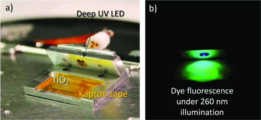
The LEDs used did not have any collimation/focusing optics on the emitting chip, hence, the sample illumination was not uniform over its area and it was difficult to calculate illuminance at particular imaging spots. The illumination profile is shown in Fig. 1(b) where paper with a fluorescent powder (UVSWG, absorption peak at 260 nm, emission peak at 525 nm) is placed instead of a sample and illuminated under 260 nm light. SEM imaging was carried out in the highest illuminance area. The UV exposure was proportional to the LED current which was used as a measure of the dose. All the experiments were carried out at maximum DUV illumination power of several W at a current of 20 mA. For the SEM imaging experiments titania (TiO2) and silicon were used as substrates for test sample fabrication.
Structures of 50 nm thick metals with different electron work functions, , (Au (5.1-5.47 eV), Ti (4.33 eV) and Al (4.06-4.26 eV)) were patterned onto the substrates using a standard electron beam lithography and lift-off process. Titania is a semi-insulating material with the electron work function of 4.9 eV Borodin and Reichling (2011), whereas Si is conductive with the work function of 4.60-4.85 eV. Silicon is a suitable substrate for SEM imaging but needs to be well grounded to facilitate removal of scattered and secondary electrons that are dispersed over the surface. For dielectric and semiconducting surfaces with low electrical conductivity the Maxwell relaxation time is long and strong charging occurs causing image distortions even though the sample is well grounded; the relaxation time is defined by the electric susceptibility and conductivity as . In our experiments, an insulating Kapton tape was placed between the samples and the sub-stage (Fig. 1(a)) to prevent removal of electrons through grounding, resulting in an increase of surface charging, hence to better reveal a charge removal effect by DUV co-illumination. The electron beam current was set to 0.4 nA and accelerating voltage of 10 kV was used for all imaging experiments, which also were in favour of an increase in surface charging.

III Results and discussion
Surface charging is the main cause of SEM image distortions when insulating materials are being imaged. It becomes a challenge to image nanometer sized structures or estimate a thickness of thin deposited layers in cross sectional imaging when conductive coatings cannot be applied.
First, surface charge removal has been tested for TiO2 substrate. The 260 nm wavelength LED light has slightly lower photon energy than the work function of titania: 4.9 eV or equivalent to a 250 nm wavelength. However, electrons from any surface defects are efficiently excited at 260 nm as it was demonstrated in the case of Ga+-ion milling under DUV illumination Gervinskas, Seniutinas, and Juodkazis (2013). SEM imaging has been tested under DUV co-illumination which is strongly absorbed at the surface. Surface defects in semiconducting and dielectric materials can be represented as defect levels in the band diagram, e.g., for the electron donor/trap typical depths are 0.1-0.3 eV below the conduction band (Fig. 2(a)). Liberation of electrons to the free vacuum level then requires correspondingly smaller photon quantum energies (slightly longer wavelengths) as compared with the work function, .
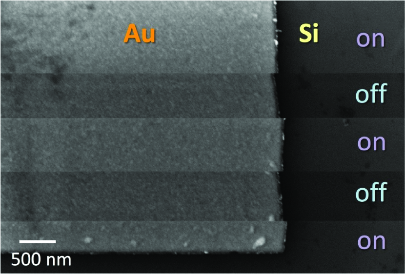
The prepared samples were placed on the sub-stage as shown in Fig. 1(a) and imaged in the SEM. A secondary electron detector operating at line averaging mode was used to better visualize image shifts resulting due to surface charging. Total scan time of one line was 26.3 ms and it took 20.2 s to acquire an entire 1024768 pixel image. The selected mode minimizes distortions in a single line as the line is scanned rapidly, but overall image obtained upon combining all the individual lines is distorted due to the charge accumulation induced drift. Images taken without and with DUV illumination are shown in Fig. 2(b) and (c), respectively. Without the DUV exposure the image drifts and becomes distorted; a contour of the actual patterned cross is indicated by the yellow dotted outline. The drift is avoided under DUV resulting in unequivocal imaging. The photoelectric effect causes any accumulated electrons to escape from the sample surface, hence, the drift is eliminated. Wide area illumination favors removal of charge gradients, hence, reduces currents, and it does not perturb the imaging electron beam. Figure 6 shows SEM image of a 50 nm thick gold structure on a silicon substrate. Deep UV illumination at 260 nm wavelength was alternatingly switched on and off during the image acquisition, which allowed to monitor changes induced by DUV exposure in situ. Clearly, the image becomes brighter when the illumination is on due to additional electrons liberated from the sample. Image drift can be qualitatively evaluated based on the edge angle changes in the ”on” and ”off” cases. The edge is straight under DUV exposure and starts to drift once the light is switched off. A clear correlation between the image drift and LED current has been confirmed.
Another advantage of DUV illumination during SEM image acquisition is the new ability to exploit material contrast. In most cases backscattered electron detection is used to obtain material contrast in SEM. Material contrast imaging with a high resolution is in demand for failure analysis in electronics Ratchev, Vandevelde, and De Wolf (2004); Coyle et al. (2009), mineralogy Gottlieb et al. (2000) and materials nano-engineering Hu et al. (2006); Bruet et al. (2008); Hibi et al. (2014). Using DUV illumination with photon energies close to the work function, materials with differing values of the work function are readily revealed. Under UV exposure the contrast between different materials appears not only due to disparate rates of secondary electron generation, but because of differences in the work function as well.
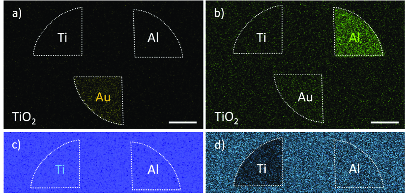
This newly proposed material contrast dependence on the work function was tested for Ti, Au and Al structures on a TiO2 substrate. Quarter-pie patterns of each metal were fabricated on the same substrate and spaced within a few microns to fit into one field of view during SEM imaging. Elemental analysis was first carried out by SEM energy dispersive x-ray spectroscopy (EDX). The elemental map identifying all three metals is provided in supplementary material Fig. S1. Oxygen signal has been observed over the Al structure indicates that the surface was oxidized and the work function has been correspondingly altered.
The quarter-pie structures were imaged with and without DUV light (Fig. 4). The acquisition contrast was optimized for the best imaging without DUV illumination. All SEM settings were kept the same when the DUV was switched on. Aluminium under illumination, due to its lowest work function (), is stripped of the largest amount of electrons and appears the darkest. Materials most deficient in electrons look darker because secondary electrons require more energy to escape them as surface potential barrier becomes higher.
A generic scaling of light - matter interaction defined by the cross section, , which determines the probability of photoelectric effect depends on the atomic number, , of the target material and the photon energy, , as Siegbahn ed. (2012) where the exponent is bound between . Hence, a stronger light matter interaction is expected for heavier elements, in our case . However, the contrast dependence is more complex.
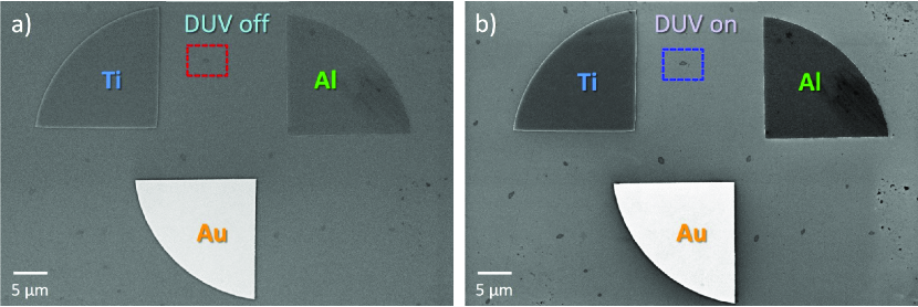
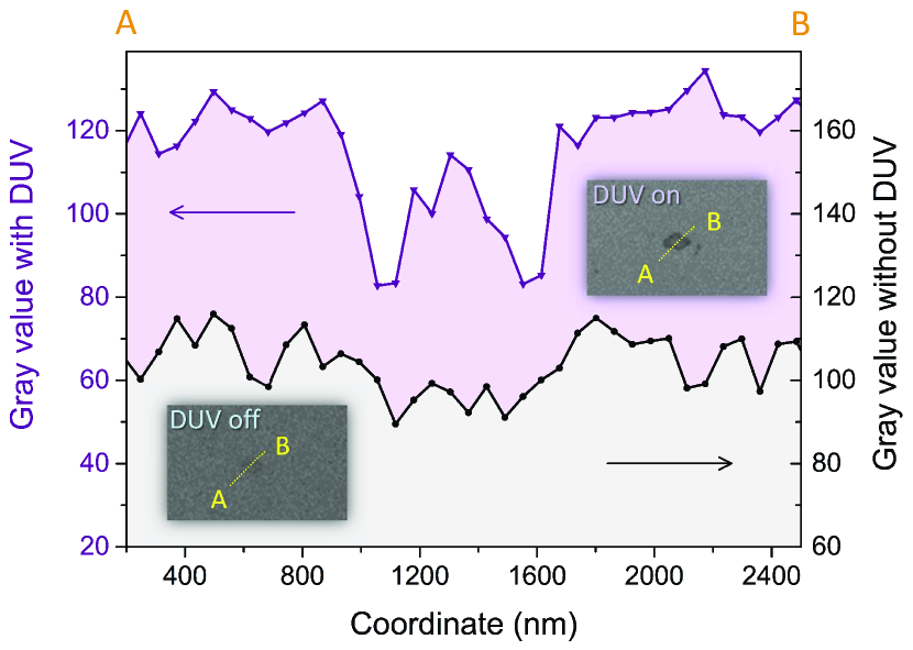
With the increased contrast between different materials, a higher resolution could be achieved. As shown in Fig. 4, the residues of poly(methyl methacrylate) resist with the work function of 4.68 eV Van Krevelen and Te Nijenhuis (2009) are resolved much better under the DUV illumination. A gray scale analysis of areas marked in Fig. 4 showed a wider dynamic range as well as larger changes in pixel signal values around the residue edges for the image taken under the illumination. The analysis graph is presented in supplementary material Fig. S2. The technique is highly appealing for nanomaterial research as better contrast due to material response yields an increase of the resolution when different materials are being imaged.
Combination of several wavelength LEDs and their availability at higher luminous fluences are expected to create new solutions for advanced SEM imaging. Deep-UV illumination incorporated into high resolution SEM microscopes could substitute the metal coating of samples for SEM imaging. This ?optical coating? will simplify and accelerate SEM imaging making it more flexible and compatible with production line inspection without damaging a chip; of special note is that the inspected chip can go into further processing steps and subsequently be imaged for a better process control feedback. Deep-UV co-illumination simultaneous with SEM imaging demonstrated here for the first time makes this technology also highly appealing for imaging of various nanomaterials. The required instrumentation to realize a LED light flood gun in a standard SEM microscope is straightforward. One could foresee DUV LEDs mounted directly inside a microscope?s vacuum chamber rather than used on a sample holder as in this proof-of-the-principle study.
IV Conclusions
Deep-UV co-illumination during SEM imaging creates a new method for contrast control via the work function of material being imaged. Moreover, SEM image distortions due to surface charging are mitigated via removal of strong charge gradients by DUV light. This method can strongly advance material research especially where high resolution imaging of dielectrics and metals placed at nanoscale proximity is required as well as for probing bio-materials where use of conductive coatings is prohibitive. Deep-UV illumination is expected to advance nanofabrication methods based on electron and ion beam techniques and substitute metal coating in imaging.
Acknowledgements.
SJ is grateful for partial support via the Australian Research Council DP130101205 Discovery project.References
- Li and Banhart (2004) J. Li and F. Banhart, Nano Letters 4, 1143 (2004).
- Muller (2009) D. A. Muller, Nature materials 8, 263 (2009).
- Yu et al. (2011) N. Yu, P. Genevet, M. A. Kats, F. Aieta, J.-P. Tetienne, F. Capasso, and Z. Gaburro, science 334, 333 (2011).
- Manfrinato et al. (2013) V. R. Manfrinato, L. Zhang, D. Su, H. Duan, R. G. Hobbs, E. A. Stach, and K. K. Berggren, Nano letters 13, 1555 (2013).
- Krivanek et al. (2010) O. L. Krivanek, M. F. Chisholm, V. Nicolosi, T. J. Pennycook, G. J. Corbin, N. Dellby, M. F. Murfitt, C. S. Own, Z. S. Szilagyi, and M. P. Oxley, Nature 464, 571 (2010).
- Wang (2000) Z. Wang, The Journal of Physical Chemistry B 104, 1153 (2000).
- Gericke et al. (2008) T. Gericke, P. Würtz, D. Reitz, T. Langen, and H. Ott, Nature Physics 4, 949 (2008).
- Joy (1984) D. C. Joy, Journal of Microscopy 136, 241 (1984).
- Orloff (1989) J. Orloff, Ultramicroscopy 28, 88 (1989).
- Van Veen et al. (2001) A. Van Veen, C. Hagen, J. Barth, and P. Kruit, Journal of Vacuum Science & Technology B 19, 2038 (2001).
- De Jonge et al. (2002) N. De Jonge, Y. Lamy, K. Schoots, and T. H. Oosterkamp, Nature 420, 393 (2002).
- Sun et al. (2012) S. Sun, K.-Y. Yang, C.-M. Wang, T.-K. Juan, W. T. Chen, C. Y. Liao, Q. He, S. Xiao, W.-T. Kung, and G.-Y. Guo, Nano letters 12, 6223 (2012).
- Gupta et al. (2014) S. Gupta, V. Moroz, L. Smith, Q. Lu, and K. C. Saraswat, IEEE Trans. Electron Dev. 61, 1222 (2014).
- IBM Press Release (2 21) IBM Press Release, “http://www-03.ibm.com/press/us/en/pressrelease/47301.wss,” (Accessed: 2015-12-21).
- Donald (2003) A. M. Donald, Nature materials 2, 511 (2003).
- Thiel and Toth (2005) B. L. Thiel and M. Toth, Journal of applied physics 97, 051101 (2005).
- Borodin and Reichling (2011) A. Borodin and M. Reichling, Physical Chemistry Chemical Physics 13, 15442 (2011).
- Gervinskas, Seniutinas, and Juodkazis (2013) G. Gervinskas, G. Seniutinas, and S. Juodkazis, Laser Phot. Rev. 7, 1049 (2013).
- Ratchev, Vandevelde, and De Wolf (2004) P. Ratchev, B. Vandevelde, and I. De Wolf, Device and Materials Reliability, IEEE Transactions on 4, 5 (2004).
- Coyle et al. (2009) R. Coyle, M. Reid, C. Ryan, R. Popowich, P. Read, D. Fleming, M. Collins, J. Punch, and I. Chatterji, in Electronic Components and Technology Conference, 2009. ECTC 2009. 59th (IEEE, 2009) pp. 423–430.
- Gottlieb et al. (2000) P. Gottlieb, G. Wilkie, D. Sutherland, E. Ho-Tun, S. Suthers, K. Perera, B. Jenkins, S. Spencer, A. Butcher, and J. Rayner, JoM 52, 24 (2000).
- Hu et al. (2006) M.-S. Hu, H.-L. Chen, C.-H. Shen, L.-S. Hong, B.-R. Huang, K.-H. Chen, and L.-C. Chen, Nature materials 5, 102 (2006).
- Bruet et al. (2008) B. J. Bruet, J. Song, M. C. Boyce, and C. Ortiz, Nature materials 7, 748 (2008).
- Hibi et al. (2014) H. Hibi, M. Yamaguchi, N. Yamamoto, and F. Ishikawa, Nano letters 14, 7024 (2014).
- Siegbahn ed. (2012) K. Siegbahn ed., Alpha-, beta-and gamma-ray spectroscopy. Vol. 1. (Elsevier, 2012).
- Van Krevelen and Te Nijenhuis (2009) D. Van Krevelen and K. Te Nijenhuis, Properties of Polymers (Elsevier Science, 2009).
V Supplement
