Crafting zero-bias one-way transport of charge and spin
Abstract
We explore the electronic structure and transport properties of a metal on top of a (weakly coupled) two-dimensional topological insulator. Unlike the widely studied junctions between topological non-trivial materials, the systems studied here allow for a unique bandstructure and transport steering. First, states on the topological insulator layer may coexist with the gapless bulk and, second, the edge states on one edge can be selectively switched-off, thereby leading to nearly perfect directional transport of charge and spin even in the zero bias limit. We illustrate these phenomena for Bernal stacked bilayer graphene with Haldane or intrinsic spin-orbit terms and a perpendicular bias voltage. This opens a path for realizing directed transport in materials such as van der Waals heterostructures, monolayer and ultrathin topological insulators.
pacs:
73.20.At; 03.65.Vf; 72.80.VpI Introduction.
More than ten years ago, the advent of graphene Novoselov et al. (2004, 2005); Zhang et al. (2005); Castro Neto et al. (2009) kickstarted the discovery of the new family of two-dimensional (2D) materials. Today, they are used as building blocks for engineering a new way back to three-dimensions, the so-called van der Waals heterostructures. Geim and Grigorieva (2013) A minimal unit with such hierarchy is a bilayer system composed of two weakly coupled layers, say and . The general Hamiltonian has the form:
| (1) |
where the intra-layer interactions encoded in the diagonal blocks dominate over the inter-layer coupling represented by the off-diagonal terms. Such arrangement may bring new possibilities which can already be noted in the case of bilayer graphene, the opening of a tunable bandgap by applying a perpendicular bias Castro et al. (2007); Oostinga et al. (2008) being a noteworthy example. Moreover, the bandgap obtained in that way may even host marginal topological states. Li et al. (2012)
Another type of bipartite system of interest includes two coupled topological insulators. Hasan and Kane (2010); Xiao et al. (2010); Ortmann et al. (2015) A typical junction involves two insulators with different topology Shevtsov et al. (2012) side by side where robust edge states develop at the interface. A less studied case is that of a 2D topological insulator (TI) weakly coupled to a metal. Recently, it was shown that edge states may survive even on a gapless bulk. Baum et al. (2015) Works addressing a non-equilibrium incarnation of TIs called Floquet topological insulators, have also pointed out that well defined topological states may exist, even on a gapless bulk. Rudner et al. (2013); Perez-Piskunow et al. (2015); Titum et al.
Here we explore the properties of a 2D metal on top of a 2D topological insulator. Although the overall system has a gapless bulk, we find that edge states do coexist and those at one edge of the TI layer can be selectively switched-off while the propagating states on the opposite edge do survive and may even keep their robustness to disorder and lattice imperfections. In a 2D TI such a selective switch-off is prevented by the bulk-boundary correspondence, a constraint which is circumvented in the composite metal on topological insulator (MOTI) system proposed here. As we will show below, the unique control of the edge states allowed by the MOTI sets the basis for one-way (directed) transport of charge and spin.
To illustrate this effect we consider bilayer graphene with either Haldane or intrinsic spin-orbit terms (ISO). Besides breaking inversion symmetry, a perpendicular bias voltage shifts the bands on each layer and can be used to generate an energy range where a 2D TI (say in the bottom layer) is weakly coupled to a metal (in the top layer). The selective switch-off of the edge states is evidenced as unpaired (non-reciprocal) edge states in the band structure which now bears a built-in asymmetry between left and right moving states. By using a three-terminal setup where two leads are connected to the bottom layer and a third lead to the top one, the built-in asymmetry can then be exploited to generate nearly perfect one-way transport of charge or spin (depending on whereas a Haldane or ISO term is considered). Interestingly, transport occurs even without a source drain bias, i.e. it can be seen as a pump effect operating without time-dependent potentials.
Two mechanisms are proposed for the selective switch-off of edge states. The first one exploits the strong sublattice polarization of the edge states together with the peculiar Bernal stacking. The stacking establishes a preferential coupling among those states polarized on the B sublattice of the TI layer and those in the A sublattice of the metal layer. In contrast, the set of states on the TI polarized on the A sublattice remain less affected by the top layer. The second mechanism is based on a geometrical setup where the top layer covers only one edge of the lower layer. While in the first case transport is fragile to perturbations, in the second case it improves when adding disorder or edge roughness, i.e. it is antifragile Taleb (2012) and thereby does not rely on the particular stacking order nor specifics of the model for the top layer, as long as it has a continuum able to hybridize with the topological states of the bottom layer. This motivates the acronym MOTI and opens the door for realizing similar phenomena in more general situations.
In the following we start by examining a spinless model of a graphene bilayer with a Haldane term. There we will see how the edge states can be selectively switched off and explain the underlying mechanism. Later on, in Sec. III, we discuss how this mechanism can be used to achieve perfect directional transport. Section IV presents a results for a bilayer with intrinsic spin-orbit coupling, a case leading to spin and valley polarized currents. Finally, we discuss the possible experimental realizations of this proposal.
II The biased Haldane bilayer: coexisting bulk and edge states.
To start with, let us analyze a graphene bilayer with a Haldane term. Haldane (1988) This spinless model will allow us to introduce the main ideas. Later on, we will consider a more realistic intrinsic spin-orbit (ISO) term. The Hamiltonian for spinless electrons is given by:
| (2) |
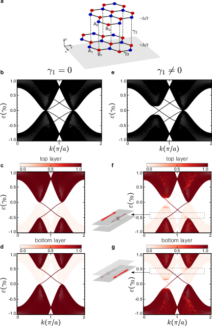
where and are the electronic creation and annihilation operators at the -orbital on site , is the nearest-neighbors matrix element and is the Haldane coupling. is () if the path from to is clockwise (anticlockwise). The on-site energies are chosen equal to () for the sites on the lower layer (upper layer) as to model a perpendicular bias. models the Bernal stacking (Fig. 1(a)) where sits on top of with the matrix element between them being .
The calculations presented here were carried out with home-made codes built on the Kwant Groth et al. (2014) module. More details on the parameters used and additional results supporting our conclusions are available in the Appendices.
To motivate the discussion let us look at the bandstructure under a strong bias voltage applied perpendicularly to the bilayer. A single of those layers bears a bulk gap with gapless Hall-like chiral states propagating along the edges. Haldane (1988) If the interlayer interaction is turned off as in Fig. 1 (b), the spectrum is the sum of that of each layer, that is, two copies of the same spectrum shifted by . When the interlayer interaction is turned on, it may be tempting to say that the main effect is to introduce a valley asymmetry close to zero energy as shown in Fig. 1 (e), an effect which has been studied in detail before. van Gelderen and Smith (2010) But, as we will see later on, there is a more striking asymmetry hidden below the gapless spectrum.
Figures 1(c–d) and (f–g) show the spectrum with a color scale encoding the weight of each state on the top (panel c and f) or bottom (panel d and g) layers, with (c-d) or without (f-g) interlayer coupling. Interestingly, in panels f and g there is a range of energies where one of the two chiral edge states is switched off (dashed rectangles).
The physical origin of this ”switch-off” relies on the hybridization of the edge states with the continuum states on the other layer. Because of the large density of states on the ungapped layer, even a coupling is enough to produce new eigenstates which have a vanishing weight on the lower layer, thereby leading to the observed switch off. The missing link is now why the switch off happens to be selective and does not act equally on all the edge states.
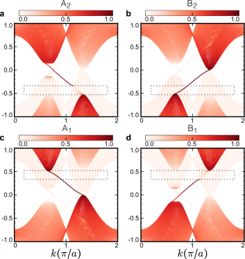
To rationalize this, let us look at the spectrum aided by a color scale resolving the different sublattices (Figs. 2a–d). One can notice a strong sublattice polarization of the edge states with values of . This is inherited from Haldane’s model and assisted by the strong bias which deters mixing between layers. Moreover, the peculiar Bernal stacking (Fig. 1(a)) introduces a difference in the environment of those sites lying on top of each other ( and ) and the others ( and ): States polarized on or will be better protected from hybridization with the states in the other layer. Therefore, those edge states polarized on sublattices and are selectively switched-off by the coupling with the continuum on the other layer. The valley where the switching off occurs depends on the bias voltage and the Haldane terms: switching the polarity of the bias or the sign of the term, changes the valley on which the states are switched-off.
III Harnessing the chiral edge state switch-off mechanism for achieving directional transport.
Could we harness this mechanism to achieve directional transport? Connecting only two leads to one of the layers (left () and right ()) does not provide the sought-for asymmetry . Even though left-right symmetry is broken because time-reversal (TRS) and inversion (IS) symmetries are broken, the required probability current conservation applied to the corresponding scattering matrix imposes . To circumvent this problem, we use a trick inspired in the physics of quantum pumps Foa Torres (2005): connecting an additional lead to the top layer (see Fig. 3(a)). Unitarity is now less restrictive on the resulting scattering matrix, thereby permiting to obtain while allowing for independent control of the occupations.
As a proof of concept, we show in Fig. 3(b) the transmittances between the and . Directional asymmetry sets in to allow for and, more interesting, when the edge states are selectively switched-off transport is almost perfectly non-reciprocal.
So far we have relied on the sublattice polarization to achieve the selective switch-off. This has the disadvantage that, for example, changing the termination from zigzag to armchair will destroy the effect. Therefore, it would be desirable to improve it in such a way that: (i) the switch-off is enhanced when adding disorder and edge roughness, and (ii) the transporting edge states keep the robustness they had in the isolated monolayer. To do this, we propose a slightly different scheme based on uncovering one of the edges at the bottom layer as represented in Fig. 3(c). This effectively decouples the corresponding edge states from the continuum on the upper layer, thereby restoring their robustness against disorder and edge roughness. Moreover, the covered edge can still be effectively switched-off independently of the details of the termination, stacking order and specifics of the lattice on the top layer. This is illustrated in Fig. 3(d) where and are shown for a device of vacancies distributed randomnly and rough edges. Interestingly, not only do the transporting states remain robust but also transport in the opposite direction is strongly suppressed in the full span of the bulk gap.
One may wonder whether new edge states would be formed at the newly created monolayer-bilayer interface, but this is not the case as we have verified numerically. Two factors contribute to this behavior: each layer retains most of its properties because of the large bias, and the top layer is metallic preventing the application of the bulk boundary correspondence.
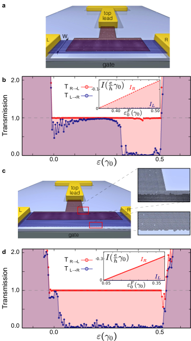
In the setup of Fig. 3(c) one observes a special feature: disorder and edge roughness tend to improve one-way transport as compared to a pristine system 111An exception being a system with perfect zigzag termination as in Fig. 1 where the edge state to be switched-off is polarized in the sublattice. (further results are included in C). This is different from merely being resilent to disorder as in the case of topological states and occurs because while the transporting edge states remain robust to disorder/roughness, the switching-off improves with it, i.e. it is antifragile. Taleb (2012)
We verified that the scattering matrix of the full system (having broken IS and TRS) is indeed non-reciprocal. But, is this enough to get a directed current at zero bias voltage? To answer this question one needs to consider the occupations at the different leads. The current flowing through lead is:
| (3) |
where , with being the top lead, and is the Fermi-Dirac distribution at lead . A similar expression holds for the left lead. To get a directed currrent, besides the non-reciprocity of the scattering matrix, the chemical potential in the third lead () needs to be different from the one on the other layer (), . Indeed, the transmittances obey the sum rule and therefore the kernel in Eq. (3) is identically zero if all the occupations are equal. In the limit of perfect switch-off of one edge state, a current exits from the right lead towards the left one even at zero bias () (see Figs. 3(b) and (d) insets).
The incoming modes that would match with the switched-off states are not backscattered but rather diverted to the upper lead. Thus, the partial scattering matrix for the two lower leads is the one of an isolator. Jalas et al. (2013) When looking at the full scattering matrix we get a circulator, Metelmann and Clerk (2015) charge flows from to to but not in the opposite direction. This is verified by explicit calculation of the currents (Figs. 3(b) and (d) insets) where we see that because the current injected by the right lead is compensated by a contribution of the same magnitude from to .
IV Biased bilayer with ISO: Pumping pure spin currents.
Let us now consider the Hamiltonian for a graphene bilayer with intrinsic spin-orbit (ISO) interaction van Gelderen and Smith (2010); Prada et al. (2011):
| (4) |
where and are the electronic creation and annihilation operators at the -orbital on site with spin up or spin down .
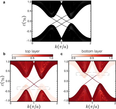
In the model of Eq. (IV) we have two copies of the spinless case considered before, one for each spin , but with an opposite phase in the second nearest neighbor term. Therefore, instead of having chiral edge states, one gets helical spin-polarized counter-propagating states. Kane and Mele (2005) Figure 4 shows the spectrum for the spinful model with a color scale encoding the weight either on the left half or the right half of the lower layer (see shaded area in the schemes). The direction of the spin polarized edge states is also indicated with arrows. Although the required spin-orbit coupling is too small in graphene, the same physics can be realized in other systems such as silicene. Ezawa (2015); Tao et al. (2015)
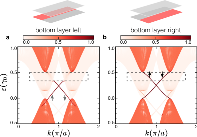
Consistently with our previous discussion one sees that the selective edge state switch-off works this time destroying the edge states with both spin projections on the same border. Interestingly, we note that in a setup like the one shown in Fig. 3, one gets a pure spin and valley current (with vanishing charge current).
Such a setup would therefore pump spin and valley from the left lead into the right one and viceversa. The direction of the valley current is inverted by inverting the polarity of the perpendicular bias. In contrast to previous proposals for spin-injection where edge states in a non-topological phase where used, Wimmer et al. (2008) here transport enjoys the robustness of the underlying topological phase.
V Summary and final remarks.
Here we present a path for crafting a non-reciprocal band-structure with edge states propagating in only one direction in a finite system. To such end we exploit the effect of placing a metal (any system with a continuum spectrum in the energy range of interest) on top of a two-dimensional system which would otherwise be a topological insulator. We show that the hybridization between the edge states on the TI and the continuum on the metal, can then be harnessed to selectively switch off the states propagating on a chosen edge of the TI.
This can be done within the same material by using, for example, a perpendicular bias voltage as shown here for bilayer graphene with spin-orbit interaction. Though pristine bilayer graphene has a small spin-orbit coupling, the following physical realizations can be envisaged:
(i) Since a stronger spin-orbit coupling is readily available in silicene or other two-dimensional materials Ezawa (2015); Tao et al. (2015) (which also have a honeycomb lattice), one can foresee a realization in a silicene sample with a graphene electrode on top;
(ii) Furthermore, even in graphene, there is theoretical and experimental evidence indicating that a spin-orbit coupling can be achieved through defects Cresti et al. (2014) or by using a specific substrate as in Ref. Calleja et al., 2015. Therefore, an alternative would be using induced spin-orbit coupling on only one layer of a bilayer sample;
Another useful result is that by using a suitable geometry, the switch off mechanism has the feature of becoming more effective with added disorder and edge-roughness, i.e. it is antifragile. An observable consequence of this effect is the generation of pure valley and spin directed currents, which can be detected through non-local transport measurements. Valenzuela and Tinkham (2006); Brune et al. (2012); Gorbachev et al. (2014) Our results may also find an application in ultrathin topological insulators, Hong et al. (2010) and van der Waals heterostructures. Geim and Grigorieva (2013)
Acknowlegdments. LEFFT and VDL acknowledge financial support from SeCyT-UNC. LEFFT acknowledges the support of the Abdus Salam International Centre for Theoretical Physics (ICTP, Trieste). VDL thanks CONICET for the fellowship. ESM acknowledges Chilean FONDECYT grant Nr. 11130129. We thank Stephan Roche and Luis Brey for useful comments on an early version of this manuscript.
Author contributions. ESM and LEFFT developed the concept and designed the study. LEFFT wrote a code and obtained the numerical results shown here, VDL verified the results. All authors discussed the results and agreed on the material to be selected for this work. LEFFT wrote the manuscript which was improved with comments and inputs from all authors.
Appendix A Localization of the edge states
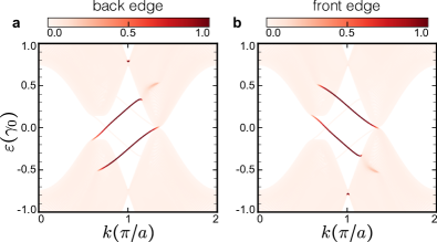
The localization of the edge states in the model introduced in the main text can be appreciated in Fig. 5. The color scale encodes the weight of each state on sites up to far away from the corresponding edge. The chirality of the edge states is evident.
Appendix B Role of the interlayer bias and other parameters used
The results shown in the main text correspond to an interlayer bias of the same magnitude as the bulk gap of the unbiased system. Here we show complementary results for a situation where the interlayer bias is smaller . The selective edge state demolition takes place over a smaller energy range but it is otherwise not compromised.
The parameters used in the text were chosen to illustrate the basic idea. Even though bilayer graphene is known for having a small spin-orbit coupling, our model offers a simple and minimal situation to illustrate the undelying physical phenomenon which, we expect, could lead to further refinement and experiments in different materials and devices.
Appendix C Additional results for the transport properties
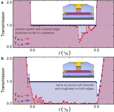
In the discussion of Fig. 3 of the main text it was mentioned that edge roughness would generally improve the selective edge state demolition for the setup of Fig. 3(c). In that situation where one edge is covered, the demolition would indeed not be effective in the full energy if the system is pristine and the corresponding edge state is polarized on the sublattice. This is illustrated in Fig. 7(a). Adding edge roughness and disorder leads to an improvement of the one-way transport as evidenced in Fig. 7(b). Thus, the demolition mechanism is anti-fragile as it improves with disorder.
References
- Novoselov et al. (2004) K. S. Novoselov, A. K. Geim, S. V. Morozov, D. Jiang, Y. Zhang, S. V. Dubonos, I. V. Grigorieva, and A. A. Firsov, “Electric field effect in atomically thin carbon films,” Science 306, 666 (2004) .
- Novoselov et al. (2005) K. S. Novoselov, A. K. Geim, S. V. Morozov, D. Jiang, M. I. Katsnelson, I. V. Grigorieva, S. V. Dubonos, and A. A. Firsov, “Two-dimensional gas of massless dirac fermions in graphene,” Nature 438, 197 (2005).
- Zhang et al. (2005) Y. Zhang, Y.-W. Tan, H. L. Stormer, and P. Kim, “Experimental observation of the quantum hall effect and berry’s phase in graphene,” Nature 438, 201 (2005).
- Castro Neto et al. (2009) A. H. Castro Neto, F. Guinea, N. M. R. Peres, K. S. Novoselov, and A. K. Geim, “The electronic properties of graphene,” Rev. Mod. Phys. 81, 109 (2009).
- Geim and Grigorieva (2013) A. K. Geim and I. V. Grigorieva, “Van der waals heterostructures,” Nature 499, 419 (2013).
- Castro et al. (2007) E. V. Castro, K. S. Novoselov, S. V. Morozov, N. M. R. Peres, J. M. B. L. dos Santos, J. Nilsson, F. Guinea, A. K. Geim, and A. H. C. Neto, “Biased bilayer graphene: Semiconductor with a gap tunable by the electric field effect,” Phys. Rev. Lett. 99, 216802 (2007).
- Oostinga et al. (2008) J. B. Oostinga, H. B. Heersche, X. Liu, A. F. Morpurgo, and L. M. K. Vandersypen, “Gate-induced insulating state in bilayer graphene devices,” Nature Materials 7, 151 (2008).
- Li et al. (2012) J. Li, I. Martin, M. Büttiker, and A. F. Morpurgo, “Marginal topological properties of graphene: a comparison with topological insulators,” Physica Scripta 2012, 014021 (2012).
- Hasan and Kane (2010) M. Z. Hasan and C. L. Kane, “Topological insulators,” Rev. Mod. Phys. 82, 3045 (2010).
- Xiao et al. (2010) D. Xiao, M.-C. Chang, and Q. Niu, “Berry phase effects on electronic properties,” Rev. Mod. Phys. 82, 1959 (2010).
- Ortmann et al. (2015) F. Ortmann, S. Roche, S. O. Valenzuela, and L. W. Molenkamp, eds., Topological Insulators: Fundamentals and Perspectives (Wiley, 2015).
- Shevtsov et al. (2012) O. Shevtsov, P. Carmier, C. Petitjean, C. Groth, D. Carpentier, and X. Waintal, “Graphene-based heterojunction between two topological insulators,” Phys. Rev. X 2, 031004 (2012).
- Baum et al. (2015) Y. Baum, T. Posske, I. C. Fulga, B. Trauzettel, and A. Stern, “Coexisting edge states and gapless bulk in topological states of matter,” Phys. Rev. Lett. 114, 136801 (2015).
- Rudner et al. (2013) M. S. Rudner, N. H. Lindner, E. Berg, and M. Levin, “Anomalous edge states and the bulk-edge correspondence for periodically-driven two dimensional systems,” Phys. Rev. X 3, 031005 (2013).
- Perez-Piskunow et al. (2015) P. M. Perez-Piskunow, L. E. F. Foa Torres, and G. Usaj, “Hierarchy of floquet gaps and edge states for driven honeycomb lattices,” Phys. Rev. A 91, 043625 (2015).
- (16) P. Titum, E. Berg, M. S. Rudner, G. Refael, and N. H. Lindner, “The anomalous floquet-anderson insulator as a non-adiabatic quantized charge pump,” arXiv:1506.00650 [cond-mat.mes-hall] .
- Taleb (2012) N. N. Taleb, Antifragile: Things That Gain from Disorder (Random House, 2012).
- Haldane (1988) F. D. M. Haldane, “Model for a quantum hall effect without landau levels: Condensed-matter realization of the parity anomaly” Phys. Rev. Lett. 61, 2015 (1988).
- Groth et al. (2014) C. W. Groth, M. Wimmer, A. R. Akhmerov, and X. Waintal, “Kwant: a software package for quantum transport,” New Journal of Physics 16, 063065 (2014).
- van Gelderen and Smith (2010) R. van Gelderen and C. M. Smith, “Rashba and intrinsic spin-orbit interactions in biased bilayer graphene,” Phys. Rev. B 81, 125435 (2010).
- Foa Torres (2005) L. E. F. Foa Torres, “Mono-parametric quantum charge pumping: Interplay between spatial interference and photon-assisted tunneling,” Phys. Rev. B 72, 245339 (2005).
- Note (1) An exception being a system with perfect zigzag termination as in Fig. 1 where the edge state to be switched-off is polarized in the sublattice.
- Jalas et al. (2013) D. Jalas, A. Petrov, M. Eich, W. Freude, S. Fan, Z. Yu, R. Baets, M. Popovic, A. Melloni, J. D. Joannopoulos, M. Vanwolleghem, C. R. Doerr, and H. Renner, “What is – and what is not – an optical isolator,” Nature Photonics 7, 579 (2013).
- Metelmann and Clerk (2015) A. Metelmann and A. A. Clerk, “Nonreciprocal photon transmission and amplification via reservoir engineering,” Phys. Rev. X 5, 021025 (2015).
- Prada et al. (2011) E. Prada, P. San-Jose, L. Brey, and H. Fertig, “Band topology and the quantum spin hall effect in bilayer graphene,” Solid State Communications 151, 1075 (2011).
- Kane and Mele (2005) C. L. Kane and E. J. Mele, “Quantum spin hall effect in graphene,” Phys. Rev. Lett. 95, 226801 (2005).
- Ezawa (2015) M. Ezawa, “Monolayer topological insulators: Silicene, germanene, and stanene,” Journal of the Physical Society of Japan, J. Phys. Soc. Jpn. 84, 121003 (2015).
- Tao et al. (2015) L. Tao, E. Cinquanta, D. Chiappe, C. Grazianetti, M. Fanciulli, M. Dubey, A. Molle, and D. Akinwande, “Silicene field-effect transistors operating at room temperature,” Nature Nanotechnology 10, 227 (2015).
- Wimmer et al. (2008) M. Wimmer, C. Adagideli, S. Berber, D. Tomanek, and K. Richter, “Spin currents in rough graphene nanoribbons: Universal fluctuations and spin injection,” Phys. Rev. Lett. 100, 177207 (2008).
- Cresti et al. (2014) A. Cresti, D. Van Tuan, D. Soriano, A. W. Cummings, and S. Roche, “Multiple quantum phases in graphene with enhanced spin-orbit coupling: From the quantum spin hall regime to the spin hall effect and a robust metallic state,” Phys. Rev. Lett. 113, 246603 (2014).
- Calleja et al. (2015) F. Calleja, H. Ochoa, M. Garnica, S. Barja, J. J. Navarro, A. Black, M. M. Otrokov, E. V. Chulkov, A. Arnau, A. L. Vazquez de Parga, F. Guinea, and R. Miranda, “Spatial variation of a giant spin-orbit effect induces electron confinement in graphene on pb islands,” Nature Physics 11, 43 (2015).
- Valenzuela and Tinkham (2006) S. O. Valenzuela and M. Tinkham, “Direct electronic measurement of the spin hall effect,” Nature 442, 176 (2006).
- Brune et al. (2012) C. Brune, A. Roth, H. Buhmann, E. M. Hankiewicz, L. W. Molenkamp, J. Maciejko, X.-L. Qi, and S.-C. Zhang, “Spin polarization of the quantum spin hall edge states,” Nature Physics 8, 485 (2012).
- Gorbachev et al. (2014) R. V. Gorbachev, J. C. W. Song, G. L. Yu, A. V. Kretinin, F. Withers, Y. Cao, A. Mishchenko, I. V. Grigorieva, K. S. Novoselov, L. S. Levitov, and A. K. Geim, “Detecting topological currents in graphene superlattices,” Science 346, 448 (2014).
- Hong et al. (2010) S. S. Hong, W. Kundhikanjana, J. J. Cha, K. Lai, D. Kong, S. Meister, M. A. Kelly, Z.-X. Shen, and Y. Cui, “Ultrathin topological insulator bi2se3 nanoribbons exfoliated by atomic force microscopy,” Nano Lett. 10, 3118 (2010).