Indirect excitons in a potential energy landscape created by a perforated electrode
Abstract
We report on the principle and realization of an excitonic device: a ramp that directs the transport of indirect excitons down a potential energy gradient created by a perforated electrode at constant voltage. The device provides an experimental proof of principle for controlling exciton transport with electrode density gradients. We observed that the exciton transport distance along the ramp increases with increasing exciton density. This effect is explained in terms of disorder screening by repulsive exciton-exciton interactions.
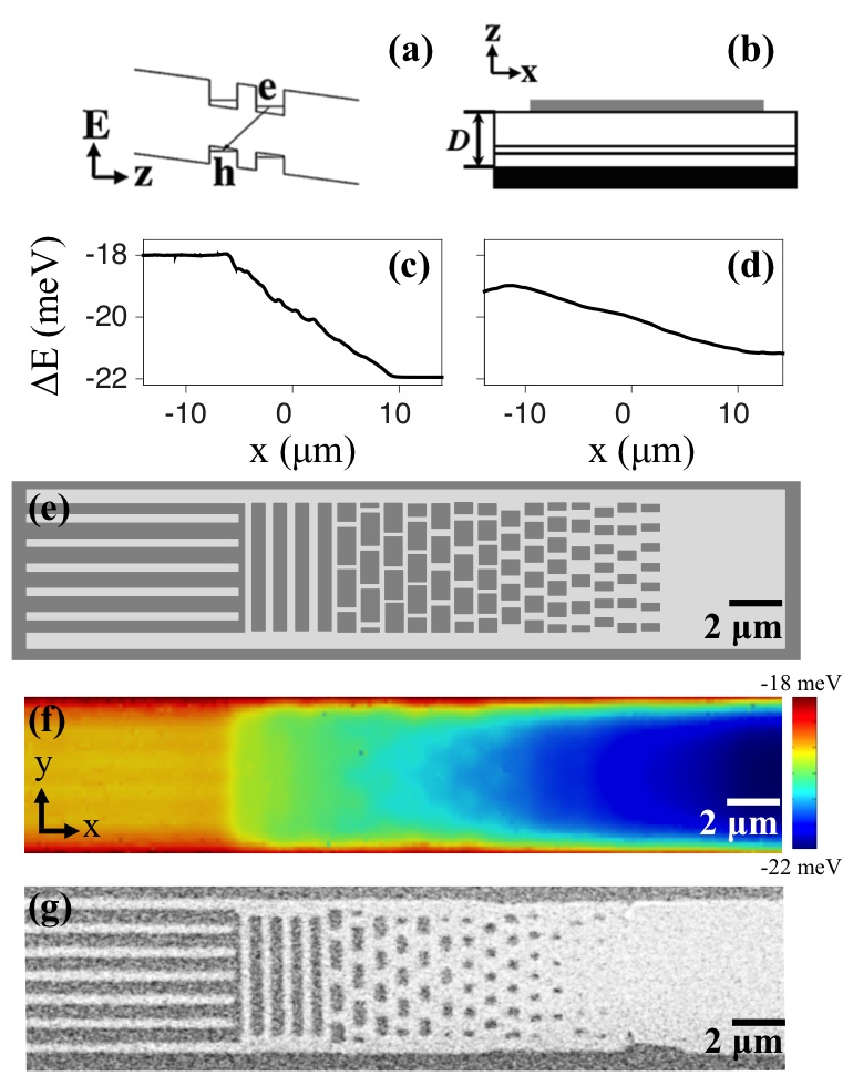
An indirect exciton (IX) is a bound state of an electron and hole in spatially separated quantum wells (QWs) [Fig. 1(a)]. The spatial separation reduces the overlap of the electron and hole wavefunctions, resulting in IX lifetimes that are orders of magnitude longer than those of direct excitons. Long lifetimes enable the IXs to travel over large distances before recombination Hagn95 ; Butov98 ; Larionov00 ; Butov02 ; Voros05 ; Ivanov06 ; Gartner06 ; Hammack09 ; Lasic10 ; Dubin11 ; Dubin12 ; Lasic14 . Due to the spatial separation, the IXs also acquire a built-in dipole moment , where is the approximate distance between the QW centers. The dipole moment can be explored to control the IX energy: an electric field applied perpendicular to the QW plane shifts the IX energy by . Miller85 These properties are advantageous for creating excitonic devices and studying the transport of IXs in electrostatic in-plane potential landscapes .
IX transport has been studied in various potential landscapes that were created by laterally modulated voltage . These potential landscapes include ramps Hagn95 ; Gartner06 ; Leonard12 , lattices Remeika09 ; Remeika12 , traps Huber98 ; High09 ; Schinner11 ; Kuznetsova15 , circuit devices High07 ; High08 ; Grosso09 ; Andreakou14 , narrow channels Grosso09 ; Vogele09 ; Cohen11 , conveyers Winbow11 , and rotating potentials Hasling15 . A set of exciton transport phenomena has been observed, including the inner ring in exciton emission patterns Butov02 ; Ivanov06 ; Hammack09 ; Dubin12 ; Stern08 ; Ivanov10 , transistor effect for excitons High07 ; High08 ; Grosso09 ; Andreakou14 , exciton localization-delocalization transition in random potentials Butov02 ; Ivanov06 ; Hammack09 , lattices Remeika09 ; Remeika12 , and moving potentials Winbow11 ; Hasling15 , coherent exciton transport with suppressed scattering High12 ; Alloing14 , and both spin transport and textures High13 .
An alternative method for creating potential landscapes for IXs was proposed in Ref. Kuznetsova10 , which is based on the lateral modulation of the electrode density rather than voltage. Divergence of the electric field around the periphery of an electrode reduces the normal component . This enables one to control , and thereby the potential energy landscape for IXs, by adjusting only the electrode density while keeping the entire device at a constant, uniform voltage. This method is beneficial compared to the voltage modulation method because it does not require an energy dissipating voltage gradient. One instance of this method based on varying the electrode width – the shaped electrode method – has been used to create confining potentials for IXs in traps High09 and ramps Leonard12 ; Andreakou14 .
In this work, we present an excitonic device based on the electrode density modulation in which a potential energy gradient is created by a perforated electrode at constant voltage. One advantage of the perforated electrode method presented here is the absence of an energy dissipating voltage gradient, similar to a shaped electrode Leonard12 ; Andreakou14 . However, the perforated electrode method also has additional advantages. The shaped electrode method requires a narrow exciton channel limiting the exciton fluxes through the channel. In contrast, the perforated electrode method does not require a narrow exciton channel and allows the width of the channel to be varied independent of the energy gradient. As a result, the perforated electrode method supports larger exciton fluxes than the shaped electrode method. The perforated electrode method gives the opportunity to create versatile potential landscapes for IXs and, in particular, create channels for directing exciton fluxes with the required geometry and energy profile. We present the proof of principle demonstration of the perforated electrode method to control IX energy and fluxes. We realized a potential energy gradient, a ramp, for IXs using a single perforated electrode of constant width and demonstrated IX transport along this ramp.
IXs were photoexcited by a 633 nm HeNe laser (focused to a spot with full width half maximum 6 m) in a GaAs coupled QW structure (CQW) grown by molecular beam epitaxy [Fig. 1(a,b)]. Exciton photoluminescence (PL) was measured by a spectrometer and a liquid-nitrogen cooled CCD. In the CQW structure, an -GaAs layer with = cm-3 serves as a homogeneous ground plane. Two 8 nm GaAs QWs are separated by a 4 nm Al0.33Ga0.67As barrier and positioned 100 nm above the -GaAs layer within an undoped m thick Al0.33Ga0.67As layer [Fig. 1(b)]. The CQWs are positioned close to the homogeneous electrode to suppress the in-plane electric field Hammack06 , which could otherwise lead to exciton dissociation Zimmermann97 . The top semitransparent electrode was fabricated by applying 2 nm Ti, 7 nm Pt, and 2 nm Au.
Figure 1(e) and 1(g) show a schematic of the electrode pattern and an SEM image of the electrode, respectively. The local electrode density, which controls the normal component and, in turn, the IX energy shift , is determined by the fraction of the area perforated. The modulation of the electrode density along is designed to create a ramp potential for IXs with a nearly linear energy gradient [Fig. 1(c),(f)]. Figure 1(c) and (f) show that the perforated electrode creates a smooth ramp potential with the energy variations due to the perforations meV, significantly smaller than meV random potential fluctuations in the CQWs Remeika09 . Such energy variations due to the perforations create no substantial obstacles for the exciton transport along the ramp as confirmed by the IX transport measurement described below; perforations create a smooth potential with no significant obstacles for the exciton transport when the lateral dimensions of the perforations are comparable to (or smaller than) the intrinsic layer width in the device.
Figure 1(d) shows the measured spatial profile of the IX energy. It is quantified by the first moment of the IX PL , where is the IX PL intensity. The IX energy also includes the difference between the direct and indirect exciton binding energies, a few meV for the CQWs Butov99 . The simulated [Fig. 1(c)] and measured [Fig. 1(d)] spatial profiles of the IX energy are qualitatively similar. However, repulsively interacting IXs screen an external potential which reduces the energy gradient in the ramp [Fig. 1(d)] as discussed below.
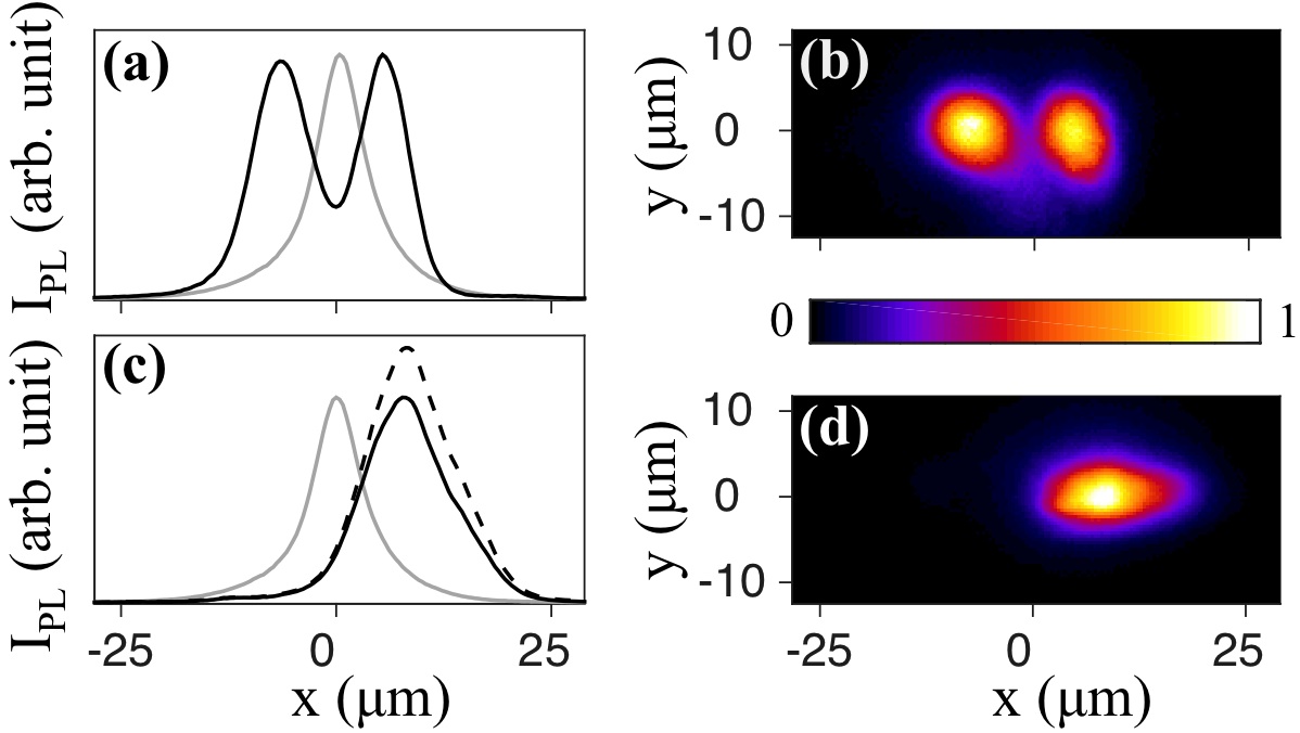
The black curve in Fig. 2(a) shows the profile of the IX PL intensity in a flat channel with no potential energy gradient. This channel was produced by a solid electrode strip of width 5 m with no perforations. The laser excitation profile is shown in gray. Figure 2(b) shows the corresponding spatial distribution of the IX PL. As there is no preferred direction of transport in the flat channel, two maxima that are nearly symmetric relative to the excitation spot position are observed. This phenomenon is consistent with the previously studied inner ring effect Butov02 ; Ivanov06 ; Hammack09 ; Dubin12 ; Stern08 ; Ivanov10 . The inner ring emission is an effect of excitons cooling down to low-energy optically active states Andreani91 as they travel away from the hot optical excitation spot. Figure 2(c) shows the profile of the IX PL intensity and Fig. 2(d) shows the spatial distribution of IX PL in the ramp. The IX transport in the ramp is directed toward lower IX energy. Such directed transport of IXs in the ramp is analogous to directed transport of electrons in a diode.
Since the electrode is semitransparent and the perforation density varies, the percentage of the signal transmitted through the electrode is not constant along the ramp. The dashed black line in Fig. 2(c) is an estimate of the PL intensity corrected for the varying electrode transparency. This estimation is described in supplementary materials along with other experimental details supp . The PL intensity correction due to the electrode transparency variation is quantitative and results in an enhancement of IX transport distance [Fig. 2(c)].
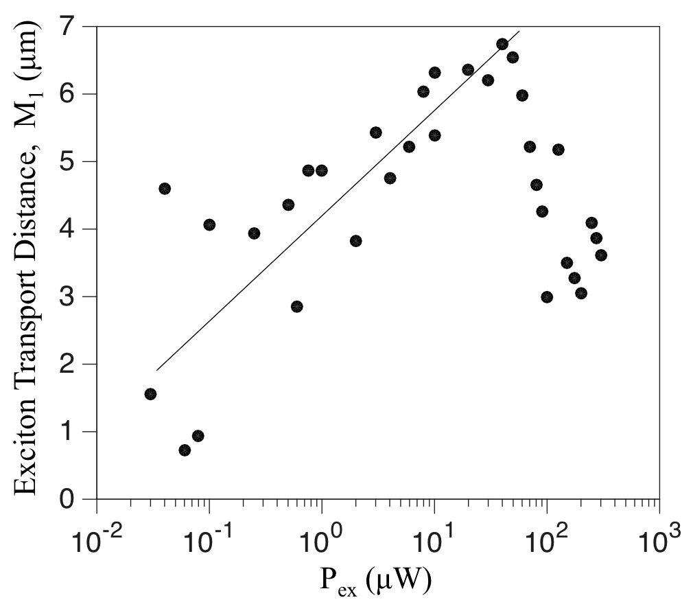
Figure 3 shows the average IX transport distance, which is quantified by the first moment of the IX PL intensity , as a function of laser excitation power . The transport distance increases with increasing up to W, an effect that can be attributed to the screening of disorder in the structure by repulsive exciton-exciton interactions. Repulsive interactions arise from the alignment of the excitons’ electric dipole moments perpendicular to the QW plane. Disorder screening improves the IX mobility and thereby increases IX transport distance along the ramp Ivanov02 ; Ivanov06 . This interpretation is supported by a theoretical model presented below. A drop of observed at the highest can be related to a photoexcitation induced reduction of .
The transport of IXs was simulated for a smooth potential energy gradient matching that generated by our device. In this model, the energy variations due to the perforations were neglected since they are small compared with the disorder. Similar to our previous work Leonard12 ; Andreakou14 , the following drift-diffusion equation is solved for the IX density, :
| (1) |
We treat as being homogeneous along and use , approximately matching the geometry of the ramp. The first and second terms in the square brackets in Eqn. (1) are due to IX diffusion and drift, respectively. The diffusion coefficient, , accounts for the screening of the intrinsic QW disorder potential by repulsively interacting IXs and is given by the thermionic model, . Here, is the amplitude of the disorder potential and is the exciton temperature. The exciton-exciton interaction potential is approximated by with where is the background dielectric constant and is the static dipole moment, corresponding to the center to center distance of the QWs. Ivanov02 ; Ivanov06 ; Ivanov10 The drift term in Eqn. (1) has contributions from the exciton-exciton interactions and the ramp potential, . A generalized Einstein relationship defines the IX mobility, where is the quantum degeneracy temperature. The exciton generation rate, , has a Gaussian profile whose width matches that of the laser excitation spot. is the IX optical lifetime and includes the fact that only low energy excitons inside the light cone may couple to light. Andreani91 The IX temperature, , is determined by a thermalization equation,
| (2) |
Here, is the heating due to the laser which is characterized by the excess energy of photoexcited excitons, . describes cooling by the emission of bulk longitudinal acoustic phonons. Model parameters and details of the calculation of , and can be found in Refs. Hammack09 ; Ivanov02 ; Ivanov06 . The coupled equations (1-2) describing the IX transport and thermalization kinetics are integrated in time until steady state solutions are obtained. The IX PL intensity is then calculated from the IX decay rate, taking into account the aperture angle of the CCD in the experiment.
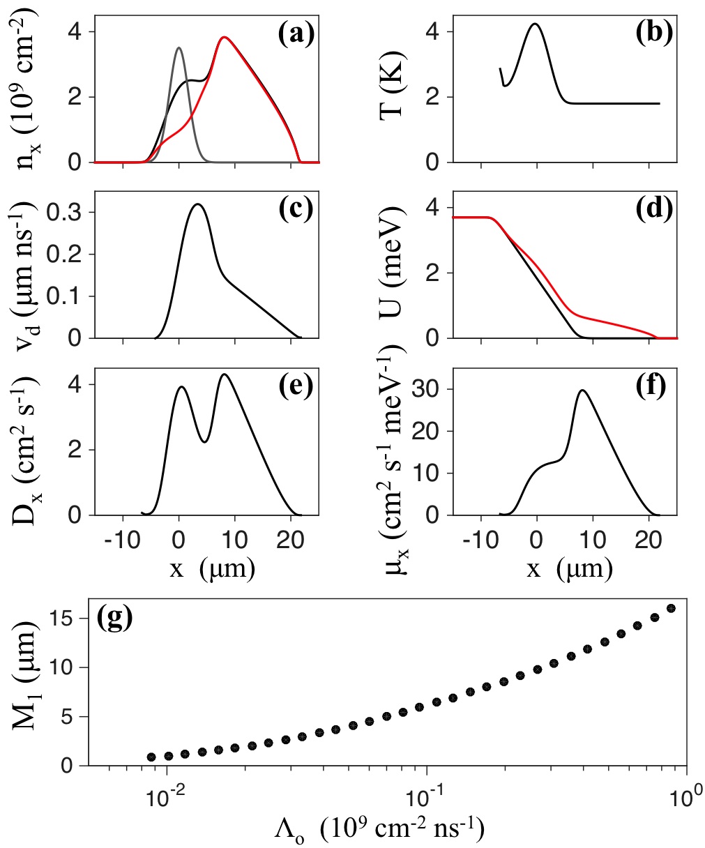
The results of the simulations are presented in Fig. 4. Figure 4(a) shows the IX density and PL intensity profiles. The simulated IX PL intensity profile [Fig. 4(a)] is in qualitative agreement with the experiment [Fig. 2(c)]. Figure 4(b) shows an enhancement of the IX temperature in the excitation spot. Figure 4(d) shows the bare ramp potential and the ramp potential with screening effects from the exciton-exciton repulsion taken into account . Figures 4(c), 4(e), and 4(f) show the IX drift velocity, diffusion coefficient, and mobility, respectively. Their values are comparable to those for IX transport in devices where no electrode perforation is involved Ivanov06 ; Hammack09 ; Leonard12 ; Andreakou14 , indicating that the perforations do not cause additional substantial obstacles for IX transport. Figure 4(g) shows the average transport distance of IXs along the ramp as a function of exciton generation rate . The units of in Fig. 4(g) can be transformed to the excitation power: /, where is the excitation spot area, is the energy of a photon in the laser excitation, and is an assumed IX-excitation probability per photon. We note that for the parameters in the experiment m2, eV, and , = 108 cm-2ns-1 transforms to = 1 W, and the calculated m at = 108 cm-2ns-1 [Fig. 4(g)] corresponds to the measured m at = 1 W [Fig. 3]. The qualitative similarities between this model and the experimental data [compare Fig. 4(a) with Fig. 2(c) and Fig. 4(g) with Fig. 3] confirms that variations in the ramp potential due to the electrode perforations are small enough to not inhibit the mobility of IXs. We note that the theory gives a nonlinear increase of the IX-transport distance with IX density [Fig. 4(g)], mainly due to the nonlinear dependence of the IX diffusion coefficient on IX density, , given above.
In summary, we report on the realization of an electrostatic ramp for indirect excitons by generating a potential energy gradient with electrode density modulation. The electrode density gradient is achieved by perforating a single electrode of constant width. In contrast to the earlier shaped electrode method, the perforated electrode method does not limit the channel width which, in turn, does not restrict the directed exciton fluxes. The perforated ramp device provides an experimental proof of principle for controlling exciton transport with electrode density gradients. The perforated electrode method gives the opportunity to create versatile potential landscapes for indirect excitons and create channels for directing exciton fluxes with the required geometry and energy profile.
This work was supported by NSF Grant No.1407277. This material is based upon work supported by the National Science Foundation Graduate Research Fellowship Program under Grant No. DGE-1144086. Y.Y.K. was supported by an Intel fellowship. J.W. was supported by EPSRC.
References
- (1) M. Hagn, A. Zrenner, G. Böhm, G. Weimann, Appl. Phys. Lett. 67, 232 (1995).
- (2) L.V. Butov, A.I. Filin, Phys. Rev. B 58, 1980 (1998).
- (3) A.V. Larionov, V.B. Timofeev, J. Hvam, K. Soerensen, Sov. Phys. JETP 90, 1093 (2000).
- (4) L.V. Butov, A.C. Gossard, D.S. Chemla, Nature 418, 751 (2002).
- (5) Z. Vörös, R. Balili, D.W. Snoke, L. Pfeiffer, K. West, Phys. Rev. Lett. 94, 226401 (2005).
- (6) A. Gärtner, A.W. Holleitner, J.P. Kotthaus, D. Schuh, Appl. Phys. Lett. 89, 052108 (2006).
- (7) A.L. Ivanov, L.E. Smallwood, A.T. Hammack, Sen Yang, L.V. Butov, A.C. Gossard, Europhys. Lett. 73, 920 (2006).
- (8) A.T. Hammack, L.V. Butov, J. Wilkes, L. Mouchliadis, E.A. Muljarov, A.L. Ivanov, A.C. Gossard, Phys. Rev. B 80, 155331 (2009).
- (9) S. Lazić, P.V. Santos, R. Hey, Phys. E 42, 2640 (2010).
- (10) M. Alloing, A. Lemaître, F. Dubin, Europhys. Lett. 93, 17007 (2011).
- (11) M. Alloing, A. Lemaître, E. Galopin, F. Dubin, Phys. Rev. B 85, 245106 (2012).
- (12) S. Lazić, A. Violante, K. Cohen, R. Hey, R. Rapaport, P.V. Santos, Phys. Rev. B 89, 085313 (2014).
- (13) D.A.B. Miller, D.S. Chemla, T.C. Damen, A.C. Gossard, W. Wiegmann, T.H. Wood, C.A. Burrus, Phys. Rev. B 32, 1043 (1985).
- (14) J.R. Leonard, M. Remeika, M.K. Chu, Y.Y. Kuznetsova, A.A. High, L.V. Butov, J. Wilkes, M. Hanson, and A.C. Gossard, Appl. Phys. Lett. 100, 231106 (2012).
- (15) M. Remeika, J.C. Graves, A.T. Hammack, A.D. Meyertholen, M.M. Fogler, L.V. Butov, M. Hanson, A.C. Gossard, Phys. Rev. Lett. 102, 186803 (2009).
- (16) M. Remeika, M.M. Fogler, L.V. Butov, M. Hanson, A.C. Gossard, Appl. Phys. Lett. 100, 061103 (2012).
- (17) T. Huber, A. Zrenner, W. Wegscheider, M. Bichler, Phys. Status Solidi A 166, R5 (1998).
- (18) A.A. High, A.K. Thomas, G. Grosso, M. Remeika, A.T. Hammack, A.D. Meyertholen, M.M. Fogler, L.V. Butov, M. Hanson, A.C. Gossard, Phys. Rev. Lett. 103, 087403 (2009).
- (19) G.J. Schinner, E. Schubert, M.P. Stallhofer, J.P. Kotthaus, D. Schuh, A.K. Rai, D. Reuter, A.D. Wieck, A.O. Govorov, Phys. Rev. B 83, 165308 (2011).
- (20) Y.Y. Kuznetsova, P. Andreakou, M.W. Hasling, J.R. Leonard, E.V. Calman, L.V. Butov, M. Hanson, A.C. Gossard. Opt. Lett. 40, 589 (2015).
- (21) A.A. High, A.T. Hammack, L.V. Butov, M. Hanson, A.C. Gossard, Opt. Lett. 32, 2466 (2007).
- (22) A.A. High, E.E. Novitskaya, L.V. Butov, A.C. Gossard, Science 321, 229 (2008).
- (23) G. Grosso, J. Graves, A.T. Hammack, A.A. High, L.V. Butov, M. Hanson, A.C. Gossard, Nature Photonics 3, 577 (2009).
- (24) P. Andreakou, S.V. Poltavtsev, J.R. Leonard, E.V. Calman, M. Remeika, Y.Y. Kuznetsova, L.V. Butov, J. Wilkes, M. Hanson, and A.C. Gossard, Appl. Phys. Lett. 104, 091101 (2014).
- (25) X.P. Vögele, D. Schuh, W. Wegscheider, J.P. Kotthaus, A.W. Holleitner, Phys. Rev. Lett. 103, 126402 (2009).
- (26) K. Cohen, R. Rapaport, P.V. Santos, Phys. Rev. Lett. 106, 126402 (2011).
- (27) A.G. Winbow, J.R. Leonard, M. Remeika, Y.Y. Kuznetsova, A.A. High, A.T. Hammack, L.V. Butov, J. Wilkes, A.A. Guenther, A.L. Ivanov, M. Hanson, A.C. Gossard, Phys. Rev. Lett. 106, 196806 (2011).
- (28) M.W. Hasling, Y.Y. Kuznetsova, P. Andreakou, J.R. Leonard, E.V. Calman, C.J. Dorow, L.V. Butov, M. Hanson, A.C. Gossard. J. Appl. Phys. 117, 023108 (2015).
- (29) M. Stern, V. Garmider, E. Segre, M. Rappaport, V. Umansky, Y. Levinson, I. Bar-Joseph, Phys. Rev. Lett. 101, 257402 (2008).
- (30) A.L. Ivanov, E.A. Muljarov, L. Mouchliadis, R. Zimmermann, Phys. Rev. Lett. 104, 179701 (2010).
- (31) A.A. High, J.R. Leonard, A.T. Hammack, M.M. Fogler, L.V. Butov, A.V. Kavokin, K.L. Campman, A.C. Gossard, Nature 483, 584 (2012).
- (32) M. Alloing, M. Beian, M. Lewenstein, D. Fuster, Y. González, L. González, R. Combescot, M. Combescot, F. Dubin, Europhys. Lett. 107, 10012 (2014).
- (33) A.A. High, A.T. Hammack, J.R. Leonard, S. Yang, L.V. Butov, T. Ostatnický, M. Vladimirova, A.V. Kavokin, T.C.H. Liew, K.L. Campman, A.C. Gossard, Phys.Rev. Lett. 110, 246403 (2013).
- (34) Y.Y. Kuznetsova, A.A. High, L.V. Butov, Appl. Phys. Lett. 97, 201106 (2010).
- (35) A.T. Hammack, N.A. Gippius, Sen Yang, G.O. Andreev, L.V. Butov, M. Hanson, A.C. Gossard, J. Appl. Phys. 99, 066104 (2006).
- (36) S. Zimmermann, A.O. Govorov, W. Hansen, J.P. Kotthaus, M. Bichler, W. Wegscheider, Phys. Rev. B 56, 13414 (1997).
- (37) Supplemental material at [URL] presenting the device potential profiles in y-direction, data corrected for semitransparency of the electrode, and data at higher temperature.
- (38) L.V. Butov, A.A. Shashkin, V.T. Dolgopolov, K.L. Campman, A.C. Gossard, Phys. Rev. B 60, 8753 (1999).
- (39) L.C. Andreani, Solid State Commun. 77, 641 (1991).
- (40) A.L. Ivanov, Europhys. Lett. 59, 586 (2002).