Bilayer SnS2: Easy-tunable Stacking Sequence by Charging and Loading Pressure
Abstract
Employing density functional theory-based methods, we investigate monolayer and bilayer structures of hexagonal SnS2, which is recently synthesized monolayer metal dichalcogenide. Comparison of 1H and 1T phases of monolayer SnS2 confirms the ground state to be the 1T phase. In its bilayer structure we examine different stacking configurations of the two layers. It is found that the interlayer coupling in bilayer SnS2 is weaker than that of typical transition-metal dichalcogenides (TMDs) so that alternative stacking orders have similar structural parameters and they are separated with low energy barriers. Possible signature of the stacking order in SnS2 bilayer has been sought in the calculated absorbance and reflectivity spectra. We also study the effects of the external electric field, charging, and loading pressure on the characteristic properties of bilayer SnS2. It is found that (i) the electric field increases the coupling between the layers at its prefered stacking order, so the barrier height increases, (ii) the bang gap value can be tuned by the external E-field and under sufficient E-field, the bilayer SnS2 can become semi-metal, (iii) the most favorable stacking order can be switched by charging and (iv) a loading pressure exceeding 3 GPa changes the stacking order. E-field tunable bandgap and easy-tunable stacking sequence of SnS2 layers make this 2D crystal structure a good candidate for field effect transistor and nanoscale lubricant applications.
pacs:
73.20.Hb, 82.45.Mp, 73.61.-r, 73.90.+f, 74.78.FkI Introduction
Ultrathin materials,Novoselov1 the study of which was boosted after the synthesis of graphene,Novoselov2 have attracted considerable interest due to their remarkable physical properties.Butler ; Chhowalla Graphene has extraordinary mechanicalLee and opticalNair properties. However, due to the lack of a band gap in graphene,Zhou exploring other two-dimensional (2D) materials with a band gap became important for several applications. In this respect, synthesis and theoretical prediction of many other 2D materials have been achieved, such as silicene,Cahangirov ; Kara germanene,Cahangirov ; Ni ; Davila ; Yang stanene,Guzman ; Bechstedt transition metal dichalcogenides (TMDs),Gordon ; Coleman ; Wang1 ; Ross ; Sahin2 ; Tongay ; Horzum ; Chen3 and hexagonal structures of III-V binary compounds (e.g. h-BN, h-AlN).Sahin3 ; Wang2 ; Kim ; Tsipas ; Bacaksiz The atomic scale of thickness of these materials led to new physical insights which suggests that possible other 2D materials may exhibit novel properties. In addition, the need for a wide range of materials for device technology makes the discovery of new layered materials essential.
In regard to search for new graphene-like or TMD-like 2D material, Sn-dichalcogenides are good candidate because of their vdW-linked lamellar crystal structure and energy bandgap which is in the visible frequency region. As a member of this family, tin disulfide (SnS2) was previously investigated in the bulk form for various applications.Fotouhi ; Parkinson1 ; Parkinson2 ; Delawski ; Schlaf ; Panda ; Ma After the emergence of novel 2D materials and improved production methods such as chemical vapor deposition, chemical and mechanical exfoliation, thinner structures of SnS2 were synthesized for different applications. For example, a few nanometer-thick hexagonal SnS2 was used for lithium storage in battery applications.Kim2 ; Seo ; Zhai ; Ma2 To enhance the electrochemical performance, composite forms of SnS2 with graphene were examined.Jiang ; Zhuo ; Qu ; Zhou2 ; Huang1 Single- and few-layer SnS2 were also used to fabricate a field-effect transistor.Pan ; De ; Song Moreover, photocatalytic character of single- and few-layer SnS2 was shown in different studies which is directly related to the optical properties of hexagonal SnS2.Chen ; Chao ; Sun ; Wei Furthermore, SnS2 nanosheet was studied for photosensitive field emission and photodetector applications.Joshi ; Xia
Recently, Zhang et al. demonstrated that photoluminescence spectrum of SnS2 and MoS2 show additional features when they form a van der Waals heterostructure which is important for the engineering of their electronic and optical properties.Zhang2 Huang et al. investigated the synthesis, characterization and the electronic properties of SnS2, from bulk to monolayer.Huang More recently, Su et al. reported that hexagonal SnS2 is a suitable material for photodetection applications with fast photocurrent response time 5 s.Su In addition to these, Ahn et al. successfully synthesized hexagonal SnS2 and orthorhombic SnS as a polymorphic 2D heterostructure.Ahn
Although there are a few number of computational works on single layer hexagonal SnS2Zhuang2 ; Xia2 , comprehensive investigation of electronic and optical properties of it’s monolayer and bilayer crystal structures are still lacking. Therefore, in this study we concentrate on the monolayer and bilayer forms of hexagonal SnS2. The structural parameters, electronic properties and optical response of these materials are investigated using ab initio methods. In addition, from the calculated absorbance or reflectivity spectra, the optical signatures which allows one to characterize the structural phase or the stacking order of the SnS2 layers were sought. Furthermore, we investigate the effects of an applied perpendicular electric field, charging, and loading pressure on the characteristic properties of bilayer SnS2.
The paper is organized as follows: in Sec. II we give details of our computational methodology. An overview of the structural phases, the electronic and optical properties of monolayer hexagonal SnS2 are presented in Sec. III. In Sec. IV different stacking orders of bilayer SnS2 in the T-phase are investigated in detail. The effect of the external electric field, charging, and loading pressure on the bilayer system are studied. Finally, we present our conclusion in Sec. V.
II Computational Methodology
Our investigations of the structural, electronic and optical properties for the layered SnS2 were performed using the Vienna ab-initio simulation package, VASPvasp1 ; vasp2 ; vasp3 which is based on density functional theory (DFT). The VASP code solves the Kohn-Sham equations for a system with periodic boundary conditions using iteratively a plane-wave basis set. The Perdew-Burke-Ernzerhof (PBE) form of the generalized gradient approximation (GGA)GGA-PBE was adopted to describe electron exchange and correlation. The hybrid DFT-HSE06 functionalHSE06 on top of GGA was used for a more accurate estimation of the band gap, as compared to GGA which usually underestimates the band gap of semiconducting systems. The spin-orbit interaction, which is essential for the TMDs, was included in the calculations. The interlayer interaction is dominated by the vdW forces for such layered materials, which was taken into account by using the DFT-D2 method of Grimme.vdW1 ; vdW2 To obtain the charge distribution of the configuration, a Bader charge analysis is used.Bader1 ; Bader2
Structural optimizations were performed with the following parameters. The kinetic energy cut-off of the plane-wave basis set was 500 eV in all calculations. The total energy difference between the sequential steps in the iterations was taken 10-5 units as convergence criterion. The convergence for the Hellmann-Feynman forces on each atom was taken to be 10-4 eV/Å. Gaussian smearing of 0.05 eV was used and the pressures on the unit cell were decreased to a value less then 1.0 kB in all three directions. For the determination of accurate charge densities, Brillouin zone integration was performed using a -centered mesh for the primitive unit cell. To avoid interactions between adjacent SnS2 monolayers and few layer systems, our calculations were performed with a large unit cell including ∼16 Å vacuum space.
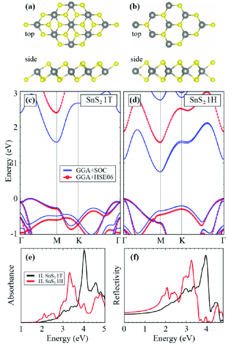
In addition, the absorbance and the reflectivity of the previously optimized structures was investigated with and without spin-orbit interaction and also including HSE06 on top of GGA. A -centered -point sampling of was used for monolayer systems. Because of the computational burden, -point sampling was reduced to for the bilayer systems, and for the calculations that include the HSE06 hybrid functional and spin-orbit interaction. The calculated dielectric function provides us with the optical quantities such as the frequency dependent absorbance and the Fresnel reflectivity through the formulas;
| (1) | ||||
| (2) |
where the dielectric function is defined as and is the frequency, is the speed of light, is the unitcell length in the perpendicular direction,
| a | c | dSn-S | Ec | E | E | |||
|---|---|---|---|---|---|---|---|---|
| (Å) | (Å) | (Å) | () | (eV) | (eV) | (eV) | (eV) | |
| 1T SnS2 | 3.68 | 2.96 | 2.59 | 0.7 | 7.53 | 3.79 | 1.58 | 2.40 |
| 1H SnS2 | 3.60 | 3.23 | 2.63 | 0.7 | 6.19 | 3.49 | 0.78 | 1.58 |
III H and T Phases of Single Layer SnS2
Monolayer SnS2 possesses two different phases 1T and 1H as shown in Fig. 1. Both phases have three trigonal subplanes where the Sn subplane is sandwiched by two S-subplanes. The 1T phase is a member of the space group where subplanes of it are stacked. The 1H is a member of the space group where subplanes of it are stacked. The lattice vectors of both phases are , where and is the lattice constant. The atomic coordinates of 1T phase are , , and for the Sn atom and the S atoms, respectively, where is the distance between the subplanes of S atoms. The atomic coordinates of 1H phase are given as , , and .
We obtained the lattice constants of 3.68 Å and 3.60 Å for 1T and 1H, respectively. The corresponding Sn-S bond lengths (dSn-S) are 2.59 Å and 2.63 Å which are given in Table 1. The energy difference between the 1T and 1H phases is meV per unit cell which shows that the formation of the 1H phase is less favorable than 1T. The cohesive energies of 1T and 1H phases are 3.79 eV and 3.49 eV, respectively. These results are consistent with the previous results which find the 1T phase the most favorable form of the monolayer. In addition, the work functions () of the phases are 7.54 eV and 6.19 eV. These work function values are larger than those of graphene and bilayer graphene (4.6 and 4.7 eV,Yu respectively) and of single- and few-layer MoS2 (5.4 eV Choi ).
Band structures of 1T and 1H phases based on GGA including spin-orbit coupling (SOC) and HSE06 hybrid functional are given in Fig. 1. The 1T phase of SnS2 monolayer has an indirect band gap where the valance band maximum (VBM) is between the and points and the conduction band minimum (CBM) is at the point. As given in Table 1, the band gap of 1T phase is 1.58 eV within GGA+SOC and 2.40 eV within GGA+HSE06. 0.7 is donated to each S atom by Sn atom. The 1H phase also has an indirect band gap where the VBM is at point and the CBM is at point. The band gap values are 0.78 eV within GGA+SOC and 1.58 eV within GGA+HSE06.
The effect of the SOC is evident in both the 1T and 1H structures, as shown in Figs. 1 (c) and (d). In the 1T structure, the splitting is 50 meV at the highest VB states at the point while in the 1H structure the splittings are 69 meV in the highest VB states at the point and 43 meV in the lowest CB states at the point. These splittings can be exploited in ‘valleytronics’ applications where the excitations of the electrons with different spin are controlled by the polarization of the incident light. This was recently demonstrated for the TMDs, especially for MoS2.Mak ; Cao
The absorbances and the reflectivities of monolayer SnS2 are also calculated and the energy dependent plots are given in Figs. 1 (e) and (f), respectively. The absorbance plot shows that the 1T and 1H phases have different characters. For the 1T phase, absorbance (black) starts at 1.8 eV, and at around 4 eV a peak is found. It has also a local maximum at around 4.5 eV. On the other hand, for the 1H phase the absorbance (red) starts at 1.7 eV and it shows its main peak around 3.2 eV, a local maximum around 4.8 eV. Since the absorbance spectra of the alternative phases are quite distinguishable, optical absorbance measurements can be a reliable tool for determining the structural phase of monolayer SnS2 samples.
IV Bilayer SnS2
Determining or controlling the stacking order of a layered material is important for electronic and optical applications. They can modify the electronic and the optical properties even if the layers are weakly interacting as in van der Waals layered materials. Improvements in synthesis techniques allows researchers to control the stacking order of multilayer structures and synthesis of devices with desired features. Therefore, in this section we investigate properties of bilayer SnS2 starting with the analysis of possible stacking orders.
| a | dL-L | E | EL-L | Ec | E | E | ||
|---|---|---|---|---|---|---|---|---|
| (Å) | (Å) | (meV) | (meV) | (eV) | (eV) | (eV) | (eV) | |
| 3.68 | 2.95 | 0 | 38 | 6.50 | 3.81 | 1.53 | 2.34 | |
| 3.68 | 2.97 | 1 | 38 | 6.50 | 3.81 | 1.47 | 2.27 | |
| 3.68 | 3.03 | 6 | 35 | 6.58 | 3.81 | 1.37 | 2.17 |
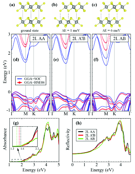
In Fig. 2, bilayer structures with three different stacking types, their corresponding band diagrams, and the imaginary part of the dielectric functions are given. In the monolayer section, the 1T phase was found to be energetically favorable, and therefore we restrict ourselves to 1T phase. (Sn atoms are aligned on Sn atoms), (S atoms are aligned on Sn atoms) and (similar with but the bottom layer is upside-down) are considered. Also the stacking (not shown) where the S atoms are aligned on S is examined, but its total energy is considerably larger as compared to the given three other stacking types. A few meV energy difference was found between the , , and stacking orders which are given in Table 2 where we have set the minimum energy to 0. All types have the same lattice constant of 3.68 Å. The interlayer distances are 2.95 Å, 2.97 Å, and 3.03 Å for the , , and stacking orders, respectively.
The cohesive energy of bilayer SnS2 in all stacking orders are the same, 3.81 eV which is slightly higher than the monolayer 1T phase. The work functions are also similar where the values are 6.50 eV, 6.50 eV and 6.58 eV for the , , and , respectively. The work function of the bilayer is smaller than that of the 1T monolayer which is in contrast with what was found for graphene and MoS2.Yu ; Choi Another point is that the interlayer potential energy per SnS2 for the different stacking types are also very close to each other; meV, meV, and meV for , , and , respectively. This weak interaction is a characteristic feature of van Waals layered materials, yet these energy values are smaller as compared to graphite (30-55 meV per atom)Liu2 ; Chen2 and typical TMDs (74, 107, 90, 126 meV per MX2 for MoS2, MoSe2, WS2, WSe2, respectively).He
In spite of the weak interlayer interactions, and the similarities of the structural parameters, the , and stacking types possess different band dispersions and band gaps. Although the VBM and the CBM are at the same symmetry points for all stacking orders, the values of the indirect band gaps are different. For , which is energetically the favorable one, we have 1.53 eV band gap within GGA and 2.34 eV within HSE06. The band gaps in the and the stackings are 1.47 and 1.37 eV within GGA and 2.27 and 2.17 eV within HSE06, respectively. It must be emphasized that the band dispersions arising from each bilayer configuration differ especially at the symmetry points and which are important for the optical transitions and the excitonic states. For stacking, the two CB edge states at the point are very close to each other as compared to those of and . On the other hand, the two CB edge states at the point are significantly different in energy as compared to those of and . The absorbance spectrum of the bilayer systems are given in Figs. 2 (g) and (h). The general trend of the absorbances for all bilayers are similar. Inset of Fig. 2 (g)is a zoom at the onset region of the absorbance spectrum. Despite the weak interactions given in Table 2, the absorbance spectra provide information on the stacking. In addition, the main peak around 4 eV of the stacking displays two distinct peaks while and have only one peak. Hence, the simple absorbance spectrum carries structural signatures although the structures are energetically very similar.
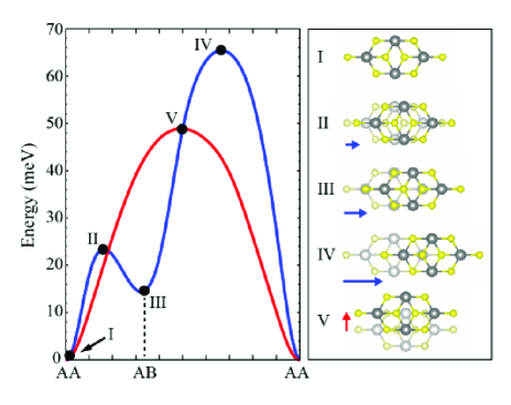
The weak layer-layer interaction in bilayer SnS2 is also promising for barrierless sliding applications. The sliding potential in the armchair and the zig-zag directions are given in Fig. 3. The local and global extrema and the corresponding structural forms are shown. The positions of the upper S atoms of the bottom layer and lower S atoms of the top layer are responsible for the potential profile. In the case of sliding along the armchair direction the local maximum is seen when the lower S atoms of the top layer are positioned at the mid point of the upper S atoms of the bottom layer. This is followed by a local minimum that corresponds to stacking. The highest point of the barrier is meV. This point is also global maximum where the S atoms from top and bottom layer are aligned on top of each other. This energy barrier is very small as compared to that of MoS2 ( meV).Tongay3 In the zig-zag direction, the barrier profile results in a symmetric peak with the highest point obtained when the S atoms of the top and bottom layers are closest to each other at the path of sliding. The maximum value of the barrier is meV. This type of barrier is common for the T phase of TMDs. Following subsections investigate how these barrier profiles are modified by electric field, charging and loading pressure.
IV.1 Effect of External Electric Field
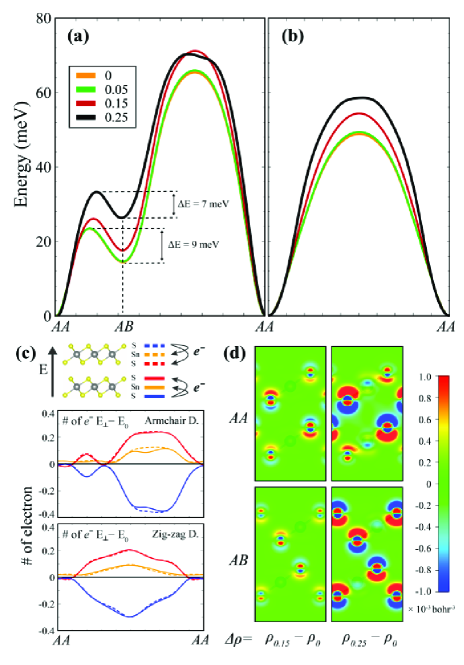
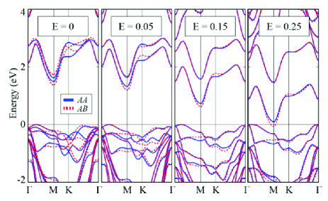
In this part, we investigate how the sliding potential is modified under the influence of an external perpendicular electric field (E-field). Three different (0.05, 0.15, 0.25 V/Å) E-field values in the positive -direction (perpendicular to the plane of bilayer system) are applied. While the energy barrier is conserved, the barrier heights increases as shown in Figs. 4 (a) and (b). The changes at 0.05 V/Å field is negligible and the profiles are almost the same as in the zero E-field case. In addition, for stacking the energy difference between the local minimum and the neighboring local maximum decreases with applied E-field. The reason of the changes can be elucidated by analyzing the variations of the charge separation in the system.
In Fig. 4 (c), by using the Bader charge analysis technique, the amount of charge difference on the atoms between the 0.25 V/Å case and the zero field case is shown along the sliding path. The solid (dashed) orange curve represents the Sn atoms at the bottom (top) layer. The solid (dashed) blue curve represents the outer S atom at the bottom (top) layer and the solid (dashed) red curve is for the inner S atom (S atoms between the sublayers of Sn atoms). The charge configurations seem to be sensitive not only to the E-field but also the stacking order of the layers. Firstly, the charge variations of the Sn atoms of the bottom and the top layers are positive which indicates that the E-field shifts electron around the Sn atoms. On the other hand, the behaviors of the changes on the S atoms are different according being at the outer or the inner part of the bilayer system. The outer S atoms have less electrons under E-field while inner S atoms attain more electrons. As an exception to these trends, the charge of the S atoms is not altered much by the E-field for the and the stackings. It needs more detailed analysis.
To clarify the effect of the external E-field on the and bilayer systems, the total charge density difference between with- and without-E-field for the cross section through the atoms in the unitcell are shown in Fig. 4(d). It seems that the S atoms are polarized by the E-field, but the Sn atoms experience no significant change. In the case of 0.15 V/Å, the polarizations are larger at the inner sides of S atoms for both and stackings. In the case of 0.25 V/Å, the polarization vanishes at the outer S atoms for stacking order. On the other hand, the polarization still exists and is enhanced at the inner S atoms of and all S atoms of stacking. More importantly, the number of electron increases gradually between the layers with electric field strength for both the and the stackings. This charge accumulation between the layers is consistent with the study of Ramasubramaniam et al.Ramasubramaniam where the MoS2 bilayer is tuned by the external E-field and the charge distribution between the layers was gradually enhanced with increasing out of plane E-field. According to our results, the perpendicular E-field increases the coupling between the SnS2 layers for stacking as compared to .
In addition, the E-field dramaticaly modifies the electronic structure of the bilayer system as shown in Fig. 5. Under the E-field, the VBM approaches to point while the CBM at point drops in energy which means that band gap decreases. The drop of band gap with E-field is slower for the stacking, so under V/Å E-field, the become semi-metal while the stacked bilayer is semiconductor with band gap 85 meV within GGA. Although this is the underestimated band gap, the trend of change on electronic structure together with enhanced stacking strength at order indicates that perpendicular E-field is useful method for tunning the band gap of bilayer SnS2 which is needed in a material for the field effect transistor application.
IV.2 Effect of Charging
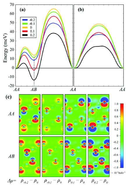
The sliding-energy barrier can also be tuned by controlling the total charge on the system. In this part, we examine the modifications of the sliding barrier by adding or subtracting electron (doping electron or hole) to the bilayer. In Figs. 6 (a) and (b), we show respectively the barriers forms along the armchair and the zig-zag directions for four different charging conditions. Positive value of charging refers to extra electrons. First of all, it is interesting that the 0.2 and also the 0.1 (per unit cell) cases result in a minimum energy for the stacking instead of . In addition, the barrier height decreases in all charging conditions and the shape of the barrier differs considerably for the armchair direction. Moreover, the maximum barrier height in the zig-zag direction decreases down to 20 meV which is comparable with the thermal energy at room temperature (25 meV).
The effect of charging can be understood by monitoring the charge localizations for and stacking. Therefore, in Fig. 6(c), the cross section of the charge density differences between the charged and the bare systems is shown for and stackings. It is expected that only positively charged regions to appear in the plot for the electron subtracted system. For the electron-added system, the expectation is the opposite. However the occurrence of both positive and negative regions for each charging case indicates that charging (positive or negative) modifies the distribution of the other electrons. In Fig. 6(c), it is explicitly seen that the inserted charges accumulate to the outer surfaces (red for positive charges and blue for the negative charges) of the bilayer system. In all cases, except the 0.2 added to stacking, the electrons (blue region) also accumulate to the region between the layers. When we compare the and stackings in all charging conditions, the lower energy case has always a larger amount of electrons (negative charge means blue region) between the layers which indicates that the interactions between the layers have covalent character.
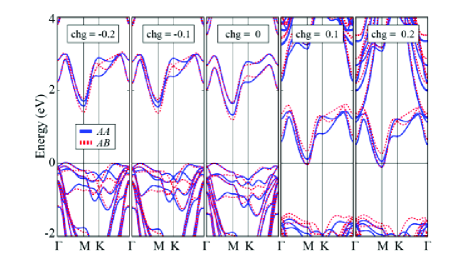
In addition, when electrons are doped, orbital of Sn atoms which mostly construct the CBM are firstly occupied as shown in Fig. 7. The energy difference between the newly occupied Sn states and the already occupied S states decreases. The change is higher for the stacking as compared to . For the hole doping case, and orbitals of S atoms which are dominant around the Fermi level (VBM) are firstly occupied. To sum up, both electron and hole doping decreases sliding barrier which makes easier to modify the stacking order, and for proper value of electron doping, favorable stacking order become stacking instead of .
IV.3 Bilayer Under Loading Pressure
The energy landscape of bilayers under constant loading pressure is studied for various 2D materials.Friction It is shown that for a given value of the applied pressure, the ratio between intralayer and interlayer interaction is a material property that describes the transition from the stick-slip to the superlubric regime. Here we study the effect of a constant loading pressure on the energy landscape of bilayer SnS2.
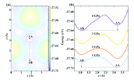
The and the stackings of bilayers, composed of materials like MoS2, have the same energy due to the symmetry of the 1H structure. However, the energy of bilayer SnS2 in 1T is different for and stackings. This is evident from the previous figures in this section as well as from Fig. 8(a) where we present the constant height energy landscape of the SnS2 bilayer. To calculate the energy landscape at constant pressure we repeat constant height scans by lowering the height by 0.2 Å steps. In this way we get the energy for the three-dimensional movement of the layers with respect to each other. We use this data to create the plots presented in Fig. 8(b). Here for a chosen loading pressure we first find the corresponding force in the -direction. Then using spline interpolation we calculate the height that gives this force for each position in the plane while moving from stacking to stacking. Interestingly, as the applied pressure is increased the relative energy difference between and stacking decreases and become even zero at 3 GPa. For pressures exceeding 3 GPa stacking becomes more favorable than stacking.
V Conclusion
Starting from the monolayer, the electronic and the optical properties of bilayer SnS2 are investigated within first principles DFT calculations. We found that the interaction between the layers is weaker than that of MoS2 and other common TMDs. We showed that although the layers interact weakly the energy band gaps and the absorbance spectra could be informative about the stacking type of the bilayer system. The energy barrier for the sliding of one layer over the other is found to be meV at its maximum which is also small as compared to MoS2.
The effect of applied E-field, charging and loading pressure on the sliding barrier of bilayer SnS2 were also studied. Under the influence of a perpendicular E-field, for the stacking which is favorable for the bilayer system, the coupling of the layer strengthens and consequently the sliding barrier height increases. In addition, it is shown that band gap of the bilayer SnS2 can be tuned by perpendicular E-field and under sufficient E-field it can be turned from semiconductor to semi-metal. On the other hand, both adding and subtracting electrons decreases the barrier. More significantly, under charging or loading pressure, stacking order can become the favorable configuration instead of stacking. Tunable bandgap makes 2D crystal of SnS2 a promising material for nanometer size field effect transistor applications. Furthermore, due to its easy-tunable stacking sequence, layered SnS2 is also a good candidate for nanoscale lubricant applications.
VI Acknowledgments
This work was supported by the bilateral project between TUBITAK (through Grant No. 113T050) and the Flemish Science Foundation (FWO-Vl). The calculations were performed at TUBITAK ULAKBIM, High Performance and Grid Computing Center (TR-Grid e-Infrastructure). CB, HS, and RTS acknowledge the support from TUBITAK Project No 114F397. H.S. is supported by a FWO Pegasus Marie Curie Fellowship. SC and AR acknowledges financial support from the Marie Curie grant FP7-PEOPLE-2013-IEF Project No. 628876, the European Research Council (ERC-2010-AdG-267374), Spanish grant, Grupos Consolidados (IT578-13). SC acknowledges support from The Scientific and Technological Research Council of Turkey (TUBITAK) under the project number 115F388.
References
- (1) K. S. Novoselov, D. Jiang, F. Schedin, T. J. Booth, V. V. Khotkevich, S. V. Morozov, and A. K. Geim, Proc. Natl. Acad. Sci. U.S.A. 102, 10451 (2005).
- (2) K. S. Novoselov, A. K. Geim, S. V. Morozov, D. Jiang, Y. Zhang, S. V. Dubonos, I. V. Grigorieva, and A. A. Firsov, Science 306, 666 (2004).
- (3) S. Z. Butler, S. M. Hollen, L. Cao, Y. Cui, J. A. Gupta, H. R. Gutié rrez, T. F. Heinz, S. S. Hong, J. Huang, A. F. Ismach, E. Johnston-Halperin, M. Kuno, V. V. Plashnitsa, R. D. Robinson, R. S. Ruoff, S. Salahuddin, J. Shan, L. Shi, M. G. Spencer, M. Terrones, W. Windl, and J. E. Goldberger, ACS Nano 7, 2898 (2013).
- (4) M. Chhowalla, H. S. Shin, G. Eda, L-J Li, K. P. Loh, H Zhang, Nat. Chem. 5, 263 (2013).
- (5) C. Lee, X. Wei, J. W. Kysar, and J. Hone, Science 321, 385 (2008).
- (6) R. R. Nair, P. Blake, A. N. Grigorenko, K. S. Novoselov, T. J. Booth, T. Stauber, N. M. R. Peres, and A. K. Geim, Science 320, 1308 (2008).
- (7) S. Y. Zhou, G. H. Gweon, J. Graf, A. V. Fedorov, C. D. Spataru, R. D. Diehl, Y. Kopelevich, D. H. Lee, S. G. Louie, A. Lanzara, Nat. Phys. 2, 595 (2006).
- (8) S. Cahangirov, M. Topsakal, E. Akturk, H. Sahin, and S. Ciraci, Phys. Rev. Lett. 102, 236804 (2009).
- (9) A. Kara, H. Enriquez, A. P. Seitsonen, L. C. L. Y. Voon, S. Vizzini, B. Aufray, and Hamid Oughaddou, Surf. Science Report. 67, 1 (2012).
- (10) Z. Ni, Q. Liu, K. Tang, J. Zheng, J. Zhou, R. Q. Z. Gao, D. Yu, and J. Lu, Nano Lett. 12, 113 (2012).
- (11) M. E. Davila, L. Xian, S. Cahangirov, A. Rubio, and G. Le Lay, New J. Phys. 16 095002 (2014).
- (12) K. Yang, S. Cahangirov, A. Cantarero, A. Rubio, and R. D’Agosta, Phys. Rev. B 89, 125403 (2014).
- (13) G. G. Guzman-Verri and L. C. Lew Yan Voon, Phys.Rev.B 76, 075131 (2007).
- (14) F. Bechstedt, L. Matthes, P. Gori, and O. Pulci, Appl. Phys. Lett. 100, 261906 (2012).
- (15) R. A. Gordon, D. Yang, E. D. Crozier, D. T. Jiang, and R. F. Frindt, Phys. Rev. B 65, 125407 (2002).
- (16) J. N. Coleman, M. Lotya, A. O’Neill, S. D. Bergin, P. J. King, U. Khan, K. Young, A. Gaucher, S. De, R. J. Smith, I. V. Shvets, S. K. Arora, J. J. Boland, J. J. Wang, J. F. Donegan, J. C. Grunlan, G. Moriarty, A. Shmeliov, R. J. Nicholls, J. M. Perkins, E. M. Grieveson, K. Theuwissen, D. W. McComb, P. D. Nellist, and V. Nicolosi, Science 331, 568 (2011).
- (17) Q. H. Wang, K. Kalantar-Zadeh, A. Kis, J. N. Coleman, and M. S. Strano, Nature Nanotech. 7, 699 (2012).
- (18) J. S. Ross, P. Klement, A. M. Jones, N. J. Ghimire, J. Yan, D. G. Mandrus, T. Taniguchi, K. Watanabe, K. Kitamura, W. Yao, D. H. Cobden, and X. Xu, Nature Nanotech. 9 268 (2014).
- (19) H. Sahin, S. Tongay, S. Horzum, W. Fan, J. Zhou, J. Li, J. Wu, and F. M. Peeters, Phys. Rev. B 87, 165409 (2013).
- (20) S. Tongay, H. Sahin, C. Ko, A. Luce, W. Fan, K. Liu, J. Zhou, Y.-S. Huang, C.-H. Ho, J. Yan, D. F. Ogletree, S. Aloni, J. Ji, S. Li, J. Li, F. M. Peeters, and J. Wu, Nat. Comm. 5 3252 (2014).
- (21) S. Horzum, D. Cakir, J. Suh, S. Tongay, Y.-S. Huang, C.-H. Ho, J. Wu, H. Sahin, and F. M. Peeters, Phys. Rev. B 89, 155433 (2014).
- (22) B. Chen, H. Sahin, A. Suslu, L. Ding, M. I. Bertoni, F. M. Peeters, and S. Tongay, ACS Nano 9, 5326 (2015).
- (23) H. Sahin, S. Changirov, M. Topsakal, E. Bekaroglu, E. Akturk, R. T. Senger, and S. Ciraci, Phys. Rev. B 80, 155453 (2009).
- (24) Q. Wang, Q. Sun, P. Jena, and Y. Kawazoe, ACS Nano 3, 621 (2009).
- (25) K. K Kim, A. Hsu, X. Jia, S. M. Kim, Y. Shi, M. Hofmann, D. Nezich, J. F. Rodriguez-Nieva, M. Dresselhaus, T. Palacios, and J. Kong, Nano Lett. 12, 161 (2012).
- (26) P. Tsipas, S. Kassavetis, D. Tsoutsou, E. Xenogiannopoulou, E. Golias, S. A. Giamini, C. Grazianetti, D. Chiappe, A. Molle, M. Fanciulli, and A. Dimoulas, Appl. Phys. Lett. 103, 251605 (2013).
- (27) C. Bacaksiz, H. Sahin, H. D. Ozaydin, S. Horzum, R. T. Senger, and F. M. Peeters, Phys. Rev. B 91, 085430 (2015).
- (28) B. Fotouhi, A. Katty, and O Gorochov, J. Electrochem. Soc. 132, 2181 (1985).
- (29) B. A. Parkinson, Langmuir 4, 967 (1988).
- (30) B. Parkinson, J. Am. Chem. Soc. 112, 7498 (1990).
- (31) E. Delawski and B. A. Parkinson, J. Am. Chem. Soc. 114, 1661 (1992).
- (32) R. Schlaf, R. D. Louder, O. Lang, C. Pettenkofer, W. Jaegermann, K. W. Nebesny, P. A. Lee, B. A. Parkinson, and N. R. Armstrong, J. Vac. Sci. Technol. A 13, 1761 (1995).
- (33) S. K. Panda, A. Antonakos, E. Liarokapis, S. Bhattacharya, and S. Chaudhuri, Mater. Res. Bull. 42, 576 (2007).
- (34) D. K. Ma, H. Y. Zhou, J. H. Zhang, and Y. T. Qian, Mater. Chem. Phys. 111, 391 (2008).
- (35) T.-J. Kim, C. Kim, D. Son, M. Choi, and B. Park, J. Power Sources 167, 529 (2007).
- (36) J.-W. Seo, J.-T. Jang, S.-W. Park, C. Kim, B. Park, and J. Cheon, Adv. Mater. 20, 4269 (2008).
- (37) C. Zhai, N. Du, and H. Z. D. Yang, Chem. Commun. 47, 1270 (2011).
- (38) J. Ma, D. Lei, L. Mei, X. Duan, Q. Li, T. Wang, and W. Zheng, CrystEngComm 14, 832 (2012).
- (39) Z. Jiang, C. Wang, G. Du, Y. J. Zhong, and J. Z. Jiang, J. Mater. Chem. 22, 9494 (2012).
- (40) L. Zhuo, Y. Wu, L. Wang, Y. Yu, X. Zhang, and F. Zhao, RSC Advances, 2, 5084 (2012).
- (41) B. Qu , C. Ma , G. Ji , C. Xu , J. Xu , Y. S. Meng, T. Wang , and J. Y. Lee, Adv. Mater. 26, 3854 (2014).
- (42) T. Zhou, W. Kong Pang, C. Zhang, J., Z. Chen, H. K. Liu, and Z. Guo, ACS Nano 8, 8323 (2014).
- (43) Z. X. Huang, Y. Wang, J. I. Wong, and H. Y. Yang, 2D Mater. 2, 024010 (2015).
- (44) T. S. Pan, D. De, J. Manongdo, A. M. Guloy, V. G. Hadjiev, Y. Lin, and H. B. Peng, Appl. Phys. Lett. 103, 093108 (2013).
- (45) D. De, J. Manongdo, S. See, V. Zhang, A. Guloy, and H. B. Peng, Nanotechnology 24, 025202 (2013).
- (46) H. S. Song, S. L. Li, L. Gao, Y. Xu, K. Ueno, J. Tang, Y. B. Cheng, and K. Tsukagoshi, Nanoscale 5, 9666 (2013).
- (47) P. Chen, Y. Su, H. Liu, and Y. Wang, ACS Appl. Mater. Interfaces 5, 12073 (2013).
- (48) J. Chao, Z. Xie, X. Duan, Y. Dong, Z. Wang, J. Xu, B. Liang, B. Shan, J. Ye, D. Chen, and G. Shen, CrystEngComm 14, 3163 (2012).
- (49) Y. Sun, H. Cheng, S. Gao, Z. Sun, Q. Liu, Q. Liu, F. Lei, T. Yao, J. He, S. Wei, and Y. Xie, Angew. Chem. Int. Ed. 51, 8727 (2012).
- (50) R. Wei, J. Hu, T. Zhou, X. Zhou, J. Liu, and J. Li, Acta Mater. 66, 163 (2014).
- (51) P. D. Joshi, C. S. Rout, D. J. Late, and D. S. Joag, J. Vac. Sci. Technol. B 33, 03C106 (2015).
- (52) J. Xia, D. Zhu, L. Wang, B. Huang, X. Huang, and X. M. Meng, Adv. Funct. Mater. 25, 4255. (2015).
- (53) X. Zhang, F. Meng, J. R. Christianson, C. Arroyo-Torres, M. A. Lukowski, D. Liang, J. R. Schmidt, and S. Jin, Nano Lett. 14, 3047 (2014).
- (54) Y. Huang, E. Sutter, J. T. Sadowski, M. Cotlet, O. L.A. Monti, D. A. Racke, M. R. Neupane, D. Wickramaratne, R. K. Lake, B. A. Parkinson, and P. Sutter, ACS Nano 8, 10743 (2014).
- (55) G. Su, V. G. Hadjiev, P. E. Loya, J. Zhang, S. Lei, S. Maharjan, P. Dong, P. M. Ajayan, J. Lou, and H. Peng, Nano Lett. 15, 506 (2015).
- (56) J.-H. Ahn, M.-J. Lee, H. Heo, J. H. Sung, K. Kim, H. Hwang, and M.-H. Jo, Nano Lett. 15, 3703 (2015).
- (57) H. L. Zhuang and R. G. Hennig, Phys. Rev. B 88, 115314 (2013).
- (58) C. Xia, Y. Peng, H. Zhang, T. Wang, S. Wei, and Y. Jia, Phys. Chem. Chem. Phys. 16, 19674 (2014).
- (59) G. Kresse and J. Hafner, Phys. Rev. B 47, 558 (1993).
- (60) G. Kresse and J. Furthmüller, Phys. Rev. B 54, 11169 (1996).
- (61) G. Kresse and D. Joubert, Phys.Rev.B 59, 1758 (1999).
- (62) J. P. Perdew, K. Burke, and M. Ernzerhof, Phys. Rev. Lett. 77, 3865 (1996).
- (63) J. Heyd, G. E. Scuseria, and M. Ernzerhof, J. Chem. Phys. 118, 8207 (2003).
- (64) S. J. Grimme, Comput. Chem. 27, 1787 (2006).
- (65) T. Bucko, J. Hafner, S. Lebegue, and J. G. Angyan, J. Phys. Chem. A 114, 11814 (2010).
- (66) G. Henkelman, A. Arnaldsson, and H. Jonsson, Comput. Mater. Sci. 36, 354 (2006).
- (67) R. F. W. Bader, Atoms in Molecules – A Quantum Theory (Oxford University Press, Oxford, UK, 1990).
- (68) Y.-J. Yu, Y. Zhao, S. Ryu, L. E. Brus, K. S. Kim, and P. Kim, Nano Lett. 9, 3430 (2009).
- (69) S. Choi, Z. Shaolin, and W. Yang, J. Korean Phys. Soc. 64, 1550 (2014).
- (70) K. F. Mak, K. He, J. Shan, and T. F. Heinz, Nature Nanotech. 7, 494 (2012).
- (71) T. Cao, G. Wang, W. Han, H. Ye, C. Zhu, J. Shi, Q. Niu, P. Tan, E. Wang, B. Liu, and J. Feng, Nat. Commun. 3, 887 (2012).
- (72) Z. Liu, J. Z. Liu, Y. Cheng, Z. Li, L. Wang, and Q. Zheng, Phys. Rev. B 85, 205418 (2012).
- (73) X. Chen, F. Tian, C. Persson, W. Duan, and N.-x. Chena, Sci Rep. 3, 3046 (2013).
- (74) J. He, K. Hummer, and C. Franchini, Phys. Rev. B 89, 075409 (2014).
- (75) S. Tongay, H. Sahin, C. Ko, A. Luce, W. Fan, K. Liu, J. Zhou, Y. S. Huang, C. H. Ho, J. Yan, D. F. Ogletree, S. Aloni, J. Ji, S. Li, J. Li, F. M. Peeters, and J. Wu, Nat. Commun. 5, 3252 (2014).
- (76) A. Ramasubramaniam, Phys. Rev. B 86, 115409 (2012).
- (77) S. Cahangirov, C. Ataca, M. Topsakal, H. Şahin, and S. Ciraci, Phys. Rev. Lett. 108, 126103 (2012).