Temperature tunability of quantum emitter - cavity coupling in a photonic wire microcavity with shielded sidewall loss
Recent technological advancements have allowed to implement in solid-state cavity-based devices phenomena of quantum nature such as vacuum Rabi splitting1; 2, controllable single photon emission3; 4 and quantum entanglement5; 6. For a sufficiently strong coupling between a quantum emitter and a cavity, large quality factors () along with small modal volume () are essential2; 7; 8. Here we show that by applying a 5nm Al coating to the sidewalls of a submicrometer-sized Fabry-Pérot microcavity, the cavity can be temperature-tuned from few hundreds at room temperatures to 2105 below 30 K. This is achieved by, first, a complete shielding of the sidewall loss with ideally reflecting lateral metallic mirrors and, secondly, a dramatic decrease of the cavity’s axial loss for small-sized devices due to the largely off-axis wavevector within the multilayered structure. Our findings offer a novel temperature-tunable platform to study quantum electrodynamical phenomena of emitter-cavity coupling. We demonstrate that a Rabi splitting of 2g=24 GHz (0.142 nm) can be readily achieved at 40 K in a 0.8m-sized device, which has an m3, comparable to best 2D photonic crystal (PhC) nanocavities2.
The physics of strong coupling between a quantum emitter and a cavity constitutes the backbone of cavity Quantum Electrodynamics (QED)9. The pioneering studies of coupling between electronic (quantum emitter) and photonic (cavity) states10; 11; 12; 13 have triggered the expansion of cavity QED from fundamental research 9 towards its solid-state implementation in laboratory devices14; 15; 3; 1; 2; 6; 4; 5 to quantum photonic circuits16; 17. The rate at which the cavity and the emitter exchange photons is crucial to determine if the system is in weak or strong coupling regime. In the first case, following Fermi’s golden rule, the free-space spontaneous emission rate of the emitter can be altered when it radiates within an electromagnetic cavity18; 11. Strong coupling manifests when the emitter and the cavity start to exchange photons coherently through a process known as vacuum Rabi oscillations8. This happens when , where are the cavity and emitter linewidths, respectively13. The strong coupling regime has gained a particular interest since it constitutes the basis of a rich spectrum of cavity QED phenomena8.
The strong coupling requires several conditions to be satisfied. First, along with a narrow linewidth, , the emitter has to possess large oscillator strength , in order to provide necessary coupling rates (). Secondly, the cavity needs to have large modal () and small volume , since scales as . Among integrated solid-state cavity structures Fabry-Pérot-type (FP) micropillars3; 19, PhC-slab nanocavities20; 2; 21, microdisks22; 23; 24 and microspheres25; 26 are the frequently utilized ones. Disk and sphere resonators offer Q’s in excess of millions but their large mode volumes make them impractical for cavity QED studies. PhC nanocavities, which offer mode volumes as small as 0.04 m3 along with reasonably high active Q’s of 20,000, require careful geometry engineering and precise technological control27.
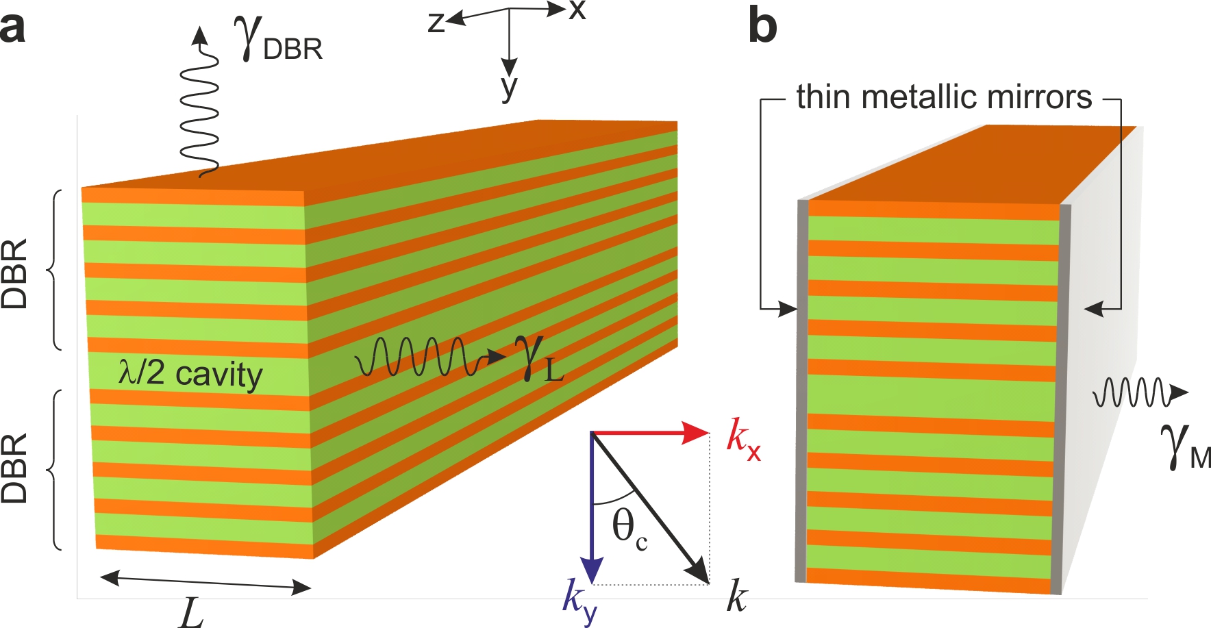
Multilayered FP microcavities, on one side, demand relatively simple and controllable technology, and, on the other side, are easily described from theoretical point of view28. In these devices tiny modal volumes may also be achieved when lateral dimensions squeeze down to several wavelengths. Here, however, sidewall losses due to scattering and poor mode confinement spoil the cavity Q severely 29; 1. Therefore, a strategy to maintain high Q’s in small-sized FP microcavities is challenging and could be beneficial to cavity QED experiments.
In the absence of material absorption, a FP microcavity is characterized by two main channels of passive loss (Fig. 1a): (i) the loss, , due to the finite reflectivity of dielectric mirrors and (ii) the lateral loss, , which accounts for both the electromagnetic (EM) wave scattering on the imperfect boundaries and radiation from dielectric cavity towards the environment. While the mode volume drops with decreasing the device size, , the lateral loss grows exponentially. This leads to a situation where the ratio , and hence the coupling rate passes a maximum at an optimal device size1.
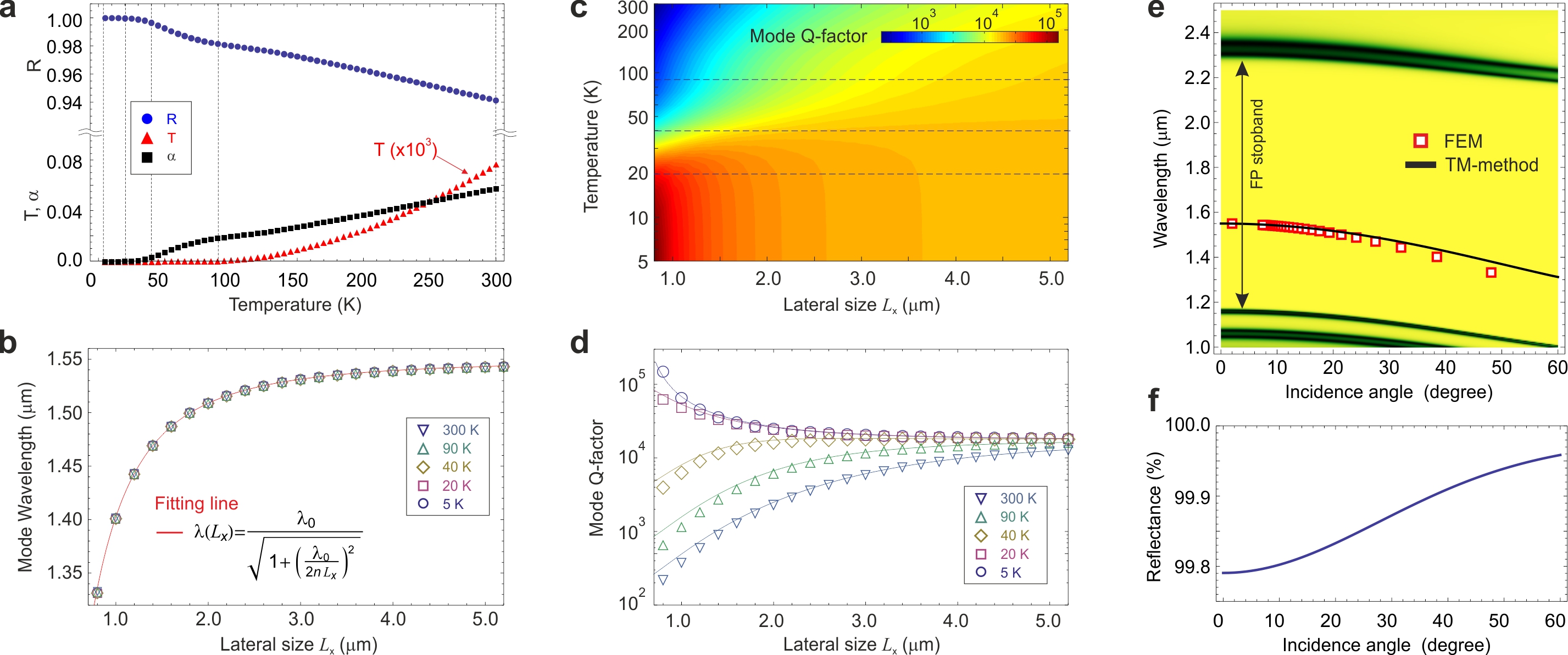
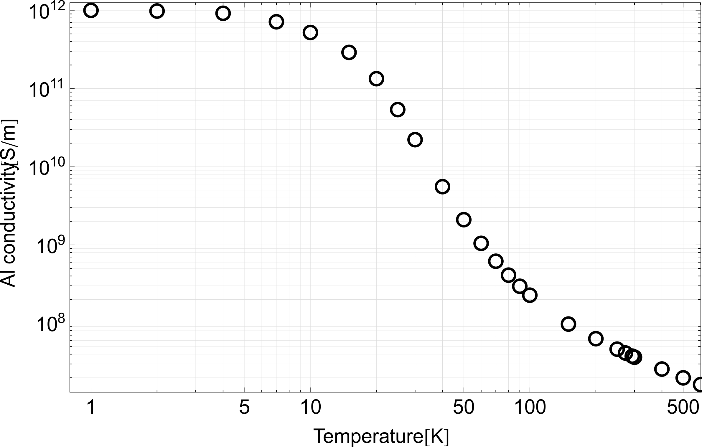
An efficient isolation of the EM mode from the environment would be ideal to prevent the mode Q from degradation. This, for example, can be achieved by applying highly reflecting mirrors to the sidewalls of the FP cavity (Fig. 1b). For this, we studied numerically a FP multilayered microcavity, which has a finite lateral dimension and is infinite in the third dimension (see Supplementary Methods section for details). In our approach, 5 nm thick Al coatings are applied to the sidewalls of the cavity. The lateral loss is thus substituted by the loss, , of the metallic mirror. The reflectivity of Al mirrors is temperature-tunable owing to a significant increase of the electrical conductivity, , by five orders of magnitude when the material is cooled down from room temperatures to few kelvins (see Supplementary Fig. S1). In particular, we find from finite-element method (FEM) calculations that the power reflection of a near-infrared wave (1.55m) from a 5nm-thick Al sheet is R=94% at T=300 K, while the remaining power is completely absorbed within the metal (Fig. 2a). The reflectance at lower temperatures grows rapidly following to a good approximation the trend , where is the EM wave frequency and is the vacuum permittivity30; 31. The calculated is larger than 99% already at 55 K and rapidly reaches unity (R=99.998%) at liquid helium temperatures (T=5 K).
The presence of metallic mirrors has imperceptible effect on the fundamental mode wavelength, , of the FP cavity. Our calculations show that, as expected29, the resonant wavelength scales as , where is the center wavelength of the laterally infinite planar cavity with mode’s effective refractive index and thickness . Here, for simplicity, materials dielectric functions have been considered temperature-independent. Figure 2b plots a series of -curves for lateral sizes in the range from 5.2 m to 0.8 m, calculated at various temperatures. It shows that the different curves are essentially coinciding, which means that, for a given size , the cavity resonance wavelength is rather robust against temperature variation.
Quite surprisingly, we observe that in the presence of sidewall mirrors the system temperature has an unprecedented effect on the cavity Q. In a general picture, for a given lateral size, the Q grows monotonically as the temperature decreases (Fig. 2c). This improvement, however, is critically dependent on the cavity size (see also Supplementary Fig. S2). In particular, while for relatively large cavities () the change in Q amounts to a factor of two, we find an improvement of up to three orders of magnitude when the lateral size becomes smaller than the wavelength (). In fact, the Q-factor of the cavity with m (Fig. 2d) boosts from 200 to 200,000 when the structure is cooled down from 300K to 5K. We note that the dependence at room temperature is both quantitatively and qualitatively very similar for FP devices with or without metal coverage. The explanation is that in one case the Q is limited by the EM wave absorption in the metal while in the second case it is spoiled by the lateral loss from the cavity.
The remarkable result of linewidth narrowing in small-sized cavities at lower temperatures necessitates an in-depth understanding of the underlaying physics. As it appears from Figs. 2c,d, below T=30K the curves invert the decreasing trend to an increasing one gaining a factor of 1000 at the smallest size of 0.8m. This implies that at low temperatures cavity losses decrease drastically – a fact, which can not be explained by only close-to-unity reflectance of sidewall mirrors. To understand fully the complex mechanism underlaying this phenomenon we refer to the definition of the mode quality factor in the form and analyze separately the two loss contributions.
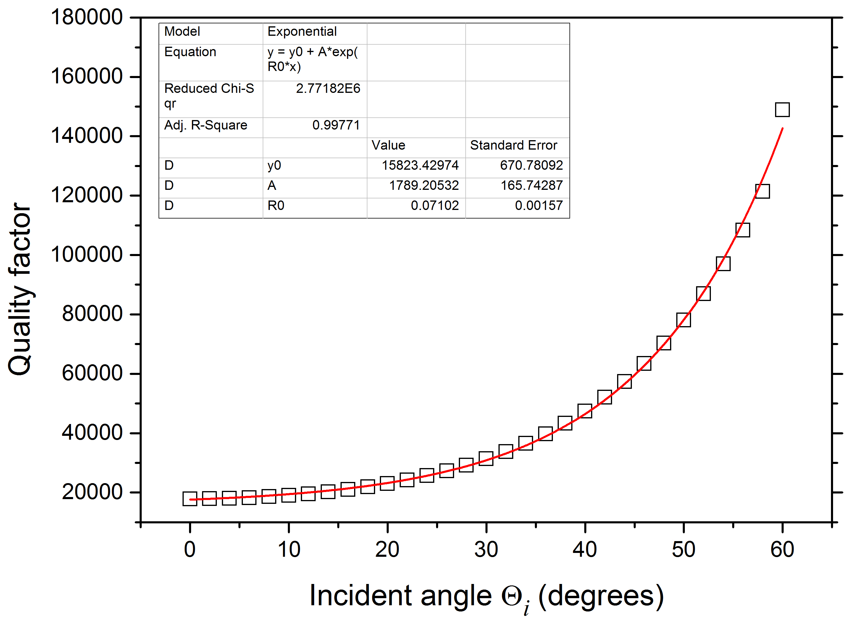
We find that the dielectric mirror’s loss decreases as the lateral size shrinks. The explanation of this unexpected result is based on the fact that a normal-incident plane -polarized wave experiences a tilted angle propagation within the multilayered dielectric structure. This angle is defined as , where and are the size-quantized and axial wavevectors, respectively. According to the definition, increases continuously as the lateral wavevector grows at smaller . In terms of wave transmission, this is equivalent to the behavior of an infinite () 1D FP microcavity under an -wave excitation at an external incidence angle , which is related to according to Snell’s law . Figure 2e shows the reflection spectrum of an infinite FP microcavity under -polarized plane wave excitation mapped for a range of incidence angles from normal to 60∘. The cavity resonance is at m at normal incidence and drifts gradually towards shorter wavelengths as grows. For comparison, FEM results for (Fig. 2b) are plotted in the same graph as scatter data. In this case and are related according to the definition. The good agreement between these results is in strong support to our explanation. Finally, in Fig. 2e we show how the reflectance of the laterally infinite dielectric mirror at the resonant wavelength grows progressively with the angle (decreasing size). In fact, Lorentzian fits to the resonant lines show that a higher reflection from multilayered mirrors leads to an exponential narrowing of linewidths, i.e. growing Q-factors (see Supplementary Fig. S3).
By considering that the metallic mirror loss is cavity size28 and temperature dependent, we model the total Q as
| (1) |
where the two loss contributions are weighted for the EM field intensity in axial () and lateral () directions. Here, is the saturation loss at very large , while and are fitting constants. Analytical curves are shown in Fig. 2d as solid lines. The various trends have been excellently reproduced by plugging in Eq.(1) only the corresponding value of the Al mirror reflectance at a given T (seeFig. 2a).
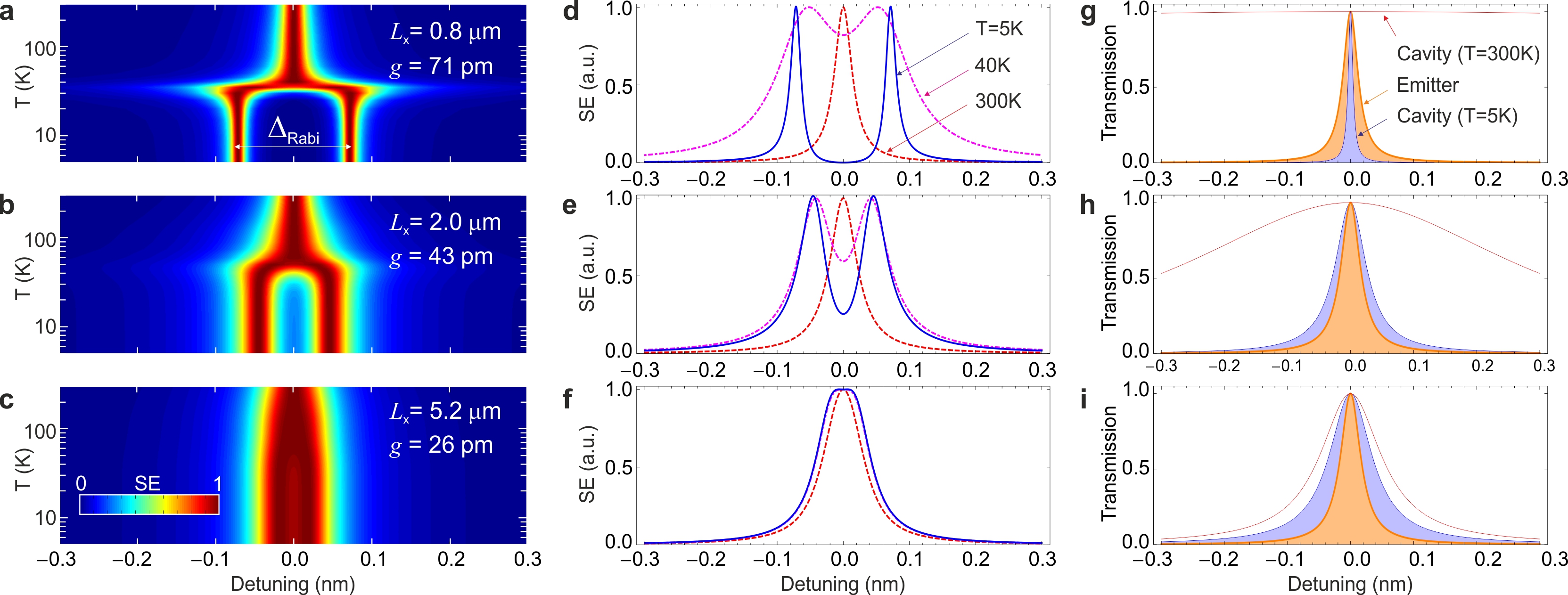
Further calculations show that, since the cavity mode volume drops linearly with , the ratio grows monotonically as the cavity gets smaller. As noted before, this property makes the metal-coated FP cavity an excellent platform for cavity QED experiments with an added value of temperature tunability. Figure 3a-c compares the calculated spontaneous emission (SE) maps of three cavities with lateral sizes m, 2.0 m and 5.2 m, respectively (see details in Supplementary Section 3). The spectra are calculated fixing the emitter linewidth14 to pm (20eV) and considering that the emitter and the cavity are always resonant, . The emitter-cavity coupling is thus defined by the ratio for the cavity of given size . These results demonstrate that a whole range of quantum couplings – from weak to strong – can be observed within a unique device by appropriately choosing the working temperature. For example, a strong Rabi splitting of pm can be readily achieved below 40 K in the smallest devices, which provide with mode volumes as small as 0.0845m3.
Figures 3d-f compare the characteristic features of the SE spectra at 300 K, 40 K and 5 K. In particular, for m size (Fig. 3d), the SE spectrum is essentially identical to the bare emitter’s line at 300 K. This is because the cavity with Q200 has minute effect on photon confinement and leads to weak coupling (Fig. 3g). Contrary to this, at 5 K the cavity linewidth is much narrower than . Here, and, thus, the strong coupling manifests as two distinctly peaked SE spectrum with a Rabi splitting that is tenfold larger than the cavity resonance width . Similar comparisons are made also for m and 5.2m cavities in Figs. 3e,h and Figs. 3f,i, respectively. In particular, we see that for the largest cavity the emitter-cavity system remains always in weak coupling regime and no notable Rabi splitting occurs even at helium temperatures. This happens because, on one side, the larger mode volume (0.613m3) and, on the other, the cavity Q, which is relatively low and stable against the temperature variation, prevent the coupling rate to be larger than .
Our findings have important implications on future cavity QED experiments, where the coupling between a quantum emitter and a cavity may be continuously tuned within the same semiconductor device. Whereas the sidewall loss shielding using thin metallic mirrors permits classical FP microcavities attaining very large ratios and circumvent the necessity in optimization, these concepts could be also extended to waveguiding configurations paving the way towards wafer-scale integrated quantum circuitry architectures.
Acknowledgments
The authors acknowledge L. Stefan and I. Carusotto for stimulating discussions. This work was partially funded by the Autonomous Province of Trento, Italy through the project “On silicon chip quantum optics for quantum computing and secure communications – SiQuro".
References
References
- (1) Reithmaier, J. P. et al. Strong coupling in a single quantum dot–semiconductor microcavity system. Nature 432, 197–200 (2004).
- (2) Yoshie, T. et al. Vacuum rabi splitting with a single quantum dot in a photonic crystal nanocavity. Nature 432, 200–203 (2004).
- (3) Pelton, M. et al. Efficient source of single photons: A single quantum dot in a micropost microcavity. Phys. Rev. Lett. 89, 233602 (2002).
- (4) Baier, M. H. et al. Single photon emission from site-controlled pyramidal quantum dots. Appl. Phys. Lett. 84, 648–650 (2004).
- (5) Michler, P. et al. A quantum dot single-photon turnstile device. Science 290, 2282–2285 (2000).
- (6) Stevenson, R. M. et al. A semiconductor source of triggered entangled photon pairs. Nature 439, 179–182 (2006).
- (7) Hendrickson, J. et al. Quantum dot photonic-crystal-slab nanocavities: Quality factors and lasing. Phys. Rev. B 72, 193303 (2005).
- (8) Khitrova, G., Gibbs, H. M., Kira, M., Koch, S. W., & Scherer, A. Vacuum rabi splitting in semiconductors. Nature Phys. 2, 81–90 (2006).
- (9) Berman, P. R. Cavity Quantum Electrodynamics. (Academic Press, Inc., Boston, 1994)
- (10) Jaynes, E. T. & Cummings, F. W. Comparison of quantum and semiclassical radiation theories with application to the beam maser. Proc. IEEE 51, 89–109 (1963).
- (11) Purcell, E. M. Spontaneous emission probabilities at radio frequencies. Phys. Rev. 69, 681 (1946).
- (12) Carmichael, H. J., Brecha, R. J., Raizen, M. G., Kimble, H. J. & Rice, P. R. Subnatural linewidth averaging for coupled atomic and cavity-mode oscillators. Phys. Rev. A 40, 5516–5519 (1989).
- (13) Andreani, L. C., Panzarini, G. & Gérard, J.-M. Strong-coupling regime for quantum boxes in pillar microcavities: Theory. Phys. Rev. B 60, 13276–13279 (1999).
- (14) Hennessy, K. et al. Quantum nature of a strongly coupled single quantum dot–cavity system. Nature 445, 896–899 (2007).
- (15) R. J. et al. Waveguide-coupled photonic crystal cavity for quantum dot spin readout. Opt. Express 22, 2376–2385 (2014).
- (16) Politi, A., Cryan, M. J., Rarity, J. G., Yu, S. & and O’Brien, J. L. Silica-on-silicon waveguide quantum circuits. Science 320, 646–649 (2008).
- (17) O’Brien, J. L., Furusawa, A. & Vučković, J. Photonic quantum technologies. Nature Photon. 3, 687–695 (2009).
- (18) Yablonovitch, E. Inhibited spontaneous emission in solid-state physics and electronics. Phys. Rev. Lett. 58, 2059–2062 (1987).
- (19) Gérard, J.-M. et al. Enhanced spontaneous emission by quantum boxes in a monolithic optical microcavity. Phys. Rev. Lett. 81, 1110–1113 (1998).
- (20) Akahane, Y., Asano, T., Song, B.-S. & Noda, S. High-Q photonic nanocavity in a two-dimensional photonic crystal. Nature 425, 944–947 (2003).
- (21) Ellis, B. et al. Ultralow-threshold electrically pumped quantum-dot photonic-crystal nanocavity laser. Nature Photon. 5, 297–300 (2011).
- (22) McCall, S. L., Levi, A. F. J.,Slusher, R. E., Pearton, S. J. & Logan, R. A. Whispering-gallery mode microdisk lasers. Appl. Phys. Lett. 60, 289–291 (1992).
- (23) Srinivasan, K., Borselli, M., Painter, O., Stintz, A. & Krishna, S. Cavity Q, mode volume, and lasing threshold in small diameter AlGaAs microdisks with embedded quantum dots. Opt. Express 14, 1094–1105 (2006).
- (24) Pitanti, A., Ghulinyan, M., Navarro-Urrios, D., Pucker, G. & Pavesi, L. Probing the spontaneous emission dynamics in Si-nanocrystals-based microdisk resonators. Phys. Rev. Lett. 104, 103901, (2010).
- (25) Fan, X., Palinginis, P., Lacey, S., Wang, H. & Lonergan, M. C. Coupling semiconductor nanocrystals to a fused-silica microsphere: a quantum-dot microcavity with extremely high Q factors. Opt. Letters 25, 1600–1602 (2000).
- (26) Pelton, M. & Yamamoto, Y. Ultralow threshold laser using a single quantum dot and a microsphere cavity. Phys. Rev. A 59, 2418–2421 (1999).
- (27) Song, B.-S., Noda, S., Asano, T. & Akahane, Y. Ultra-high-Q photonic double-heterostructure nanocavity. Nature Mater. 4, 207–210 (2005).
- (28) Saleh, B. E. A. & Teich, M. C. Fundamentals of Photonics: Second Edition. (John Wiley & Son, Hoboken, 2007).
- (29) Reithmaier, J. P. et al. Size dependence of confined optical modes in photonic quantum dots. Phys. Rev. Lett. 78, 378–381 (1997).
- (30) Holstein, T. Optical and infrared reflectivity of metals at low temperatures. Phys. Rev. 88, 1427 (1952).
- (31) Bennett, H. E., Silver, M. & Ashley, E. J. Infrared reflectance of aluminum evaporated in ultra-high vacuum. JOSA 53, 1089–1095 (1963).
- (32) Desai, P. D., James, H. M. and Ho, Ch. Y. Electrical resistivity of aluminum and manganese. J. Phys. Chem. Ref. Data 13, 1131–1172 (1984).
Supplementary Information
.1 Methods
.2 The dielectric structure
The multilayered structure is constituted by a stack of two quarter-wavelength dielectric materials and , with refractive indices and and thicknesses and , respectively. The laterally infinite planar cavity has a center wavelength nm. The FP microcavity is formed by sandwiching a half-wavelength layer between two 5.5-period distributed Bragg reflectors (DBR).
We notice, that any different choice for material refractive indices does not alter the findings and conclusions of this paper. In fact, all results can be reproduced for any other contrast () of refractive indices by appropriately choosing the number of DBR periods.
.3 Numerical calculations of finite size FP microcavities
Finite-elements method – The resonant frequency and the cavity Q were calculated resolving the wave equation using the COMSOL commercial software’s Eigenfrequency Domain Solver module. The temperature dependence of Al mirrors conductivity (Fig. S1) has been considered in the wave equation
| (S1) |
where and are the material relative permittivity and permeability, respectively.
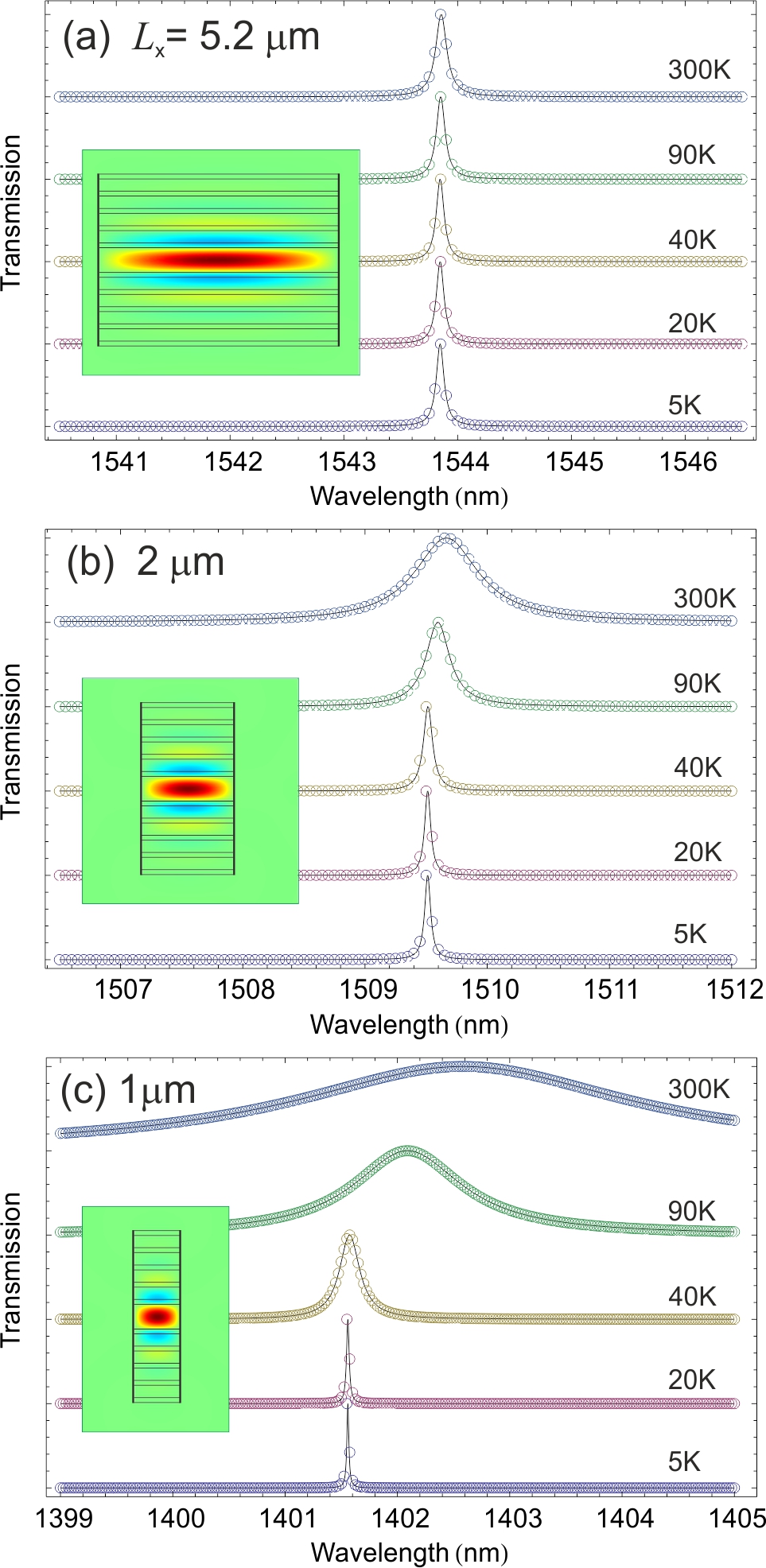
In Fig. S2a-c the fundamental modes spectral lineshape at selected temperatures is calculated for three different cavity sizes (m, 2m and 1m). The solid lines are based on constructed Lorentzian lineshapes following , where the eignefrequency and the loss were obtained from Eigenfrequency analysis.
The scattered data points () in the same graphs are the results from Frequency Domain calculations. In this approach, the power transmission of the FP microcavity is calculated by running the normal incident plane wave frequency around the expected resonance. An excellent agreement between the Eigenfrequency and Frequency Domain calculations is evident. The electric field distributions (mode shape and spatial extension) are shown as insets in corresponding graphs of Fig. S2.
.4 Linewidth narrowing in planar infinite FP cavity at oblique incidence
Transfer matrix calculations – The planar microcavities transmission spectra were calculated for the same layer stack using a home made numeric code.
In order to extract the cavity Q at oblique angles of incident plane TE-polarized wave, the following procedure has been adopted: first, the power transmission spectrum was calculated in a broad spectral range and, secondly, a Lorentzian fit was applied to the resonant transmission line. Finally, the extracted Q’s were plotted against the incident angle and fitted using an exponential function (Fig. S3).
.5 Spontaneous Emission spectrum calculations
We have calculated the Spontaneous Emission (SE) spectra using Eqs. 9,10 from Ref. 13:
| (S2) |
| (S3) |
where is the center frequency of the cavity resonance, and are the cavity and emitter linewidths, respectively, is the coupling rate. In strong coupling conditions, when and describe the doublets of Lorentzians separated by the Rabi frequency 2 and individual effective linewidths of .
The SE spectra are strongly dependent on the system temperature via and .