Ohmic contacts to 2D semiconductors through van der Waals bonding
Abstract
High contact resistances have blocked the progress of devices based on MX2 (M = Mo,W; X = S,Se,Te) 2D semiconductors. Interface states formed at MX2/metal contacts pin the Fermi level, leading to sizable Schottky barriers for p-type contacts in particular. We show that (i) one can remove the interface states by covering the metal by a 2D layer, which is van der Waals-bonded to the MX2 layer, and (ii) one can choose the buffer layer such, that it yields a p-type contact with a zero Schottky barrier height. We identify possible buffer layers such as graphene, a monolayer of h-BN, or an oxide layer with a high electron affinity, such as MoO3. The most elegant solution is a metallic layer with a high work function. A NbS2 monolayer adsorbed on a metal yields a high work function contact, irrespective of the metal, which gives a barrierless contact to all MX2 layers.
keywords:
Ohmic contact, van der Waals bonding, two dimensional materials1 Introduction
Layered transition metal dichalcogenides MX2, M = Mo,W, X = S,Se,Te, are widely explored because of their unique properties and their potential for applications in electronic devices.1, 2 MX2 monolayers are direct band gap semiconductors with band gaps in the range of 1-2 eV, which have appealing electronic and optoelectronic properties.3, 4 MX2 layers can be obtained via micro-mechanical cleaving,5 by chemical vapor deposition (CVD),6, 7 or even by spin coating precursor molecules.8 Important for applications in devices is the ability to have both electron (n-type) and hole (p-type) transport in these 2D materials. Charge carrier transport in MX2 field-effect transistors (FETs) is usually dominated by electrons; p-type transport has only been demonstrated in WSe2.9, 10
A major challenge for p-type transport is that MX2 forms a large Schottky barrier (SB) for holes with metals commonly used for making electrical contacts. A standard way to reduce a metal/semiconductor contact resistance is to heavily dope the semiconductor in the contact region, which effectively decreases the SB width. Local doping of a 2D semiconductor is however very challenging; so far most techniques used for doping 2D materials, such as substitutional doping,11 adsorbed molecules9, 12, 13, or electrolytes14, 15, have a limited spatial resolution. Alternatively one tries to decrease the SB height, essentially by covering the metal by a thin layer to increase its work function. Oxides have shown their potential for p-type contacts in organic photovoltaics and light-emitting diodes,16, 17 and have also been tested in MoS2 FETs.18, 19 Oxides have also been applied succesfully to reduce the SB height for n-type contacts to MoS2.20
Common metals generally give n-type contacts with substantial SB heights, leading to high contact resistances. Although MX2 monolayers are free of dangling bonds, nevertheless they interact with low work-function metals to form a density of interface states with energies inside the MX2 band gap, which is sufficiently large to pin the Fermi level and cause a sizable SB for electrons.21, 22, 23 We show that high work-function metals yield high SBs for holes by a similar mechanism.
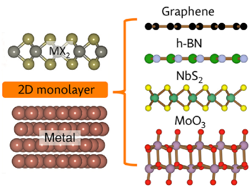
We suggest a practical way to solve the p-type contact problem and tune the SB height by inserting a monolayer of a 2D material between the metal substrate and the MX2 semiconductor, see figure 1. The buffer layer suppresses the metal/MX2 interface states. 2D materials have certain unique properties not found in buffer layers of 3D materials.5 As the interlayer bonding is van der Waals, neither the structure of the 2D buffer layer, nor that of the MX2 semiconductor, is perturbed significantly by stacking them. The 2D buffer layer need not be lattice matched to the metal or to the MX2 layer, and the structure of the multilayer will in general be incommensurate. Van der Waals interface bonding also promises the absence of interface states. Covering the metal by an adsobant layer such as graphene, a monolayer of hexagonal boron nitride (h-BN) or -MoS2, has proved to be beneficial for making n-type contacts.21, 24 We show that a 2D buffer layer can be selected to obtain a zero SB height for holes.
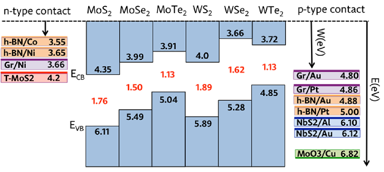
A h-BN monolayer is a buffer layer that can be used for making n-type contacts, because adsorption of h-BN on a metal decreases its work function by up to 1-2 eV.28 For instance, Co/h-BN and Ni/h-BN are predicted to form zero SB height n-type contacts to MX2 semiconductors, see figure 2.21 A decrease of the work function is unfavorable for making p-type contacts. Metal/h-BN gives a p-type contact to MX2 only if the metal work function is sufficiently high, and the MX2 ionization potential is sufficiently low. We find a zero SB height for Pt/h-BN, and Au/h-BN contacts to MoTe2 and a low SB for Pt/h-BN/WSe2, see figure 2. Alternatively, one can use a graphene buffer layer,29, 30 whose behavior is qualitatively similar to that of a h-BN monolayer.
To make more universely applicable p-type contacts, one needs a buffer layer that effectively increases the metal work function. Oxides such as MoO3 are an option. The MoO3 structure consists of bilayers, making it conceivable to cover a metal with a single MoO3 bilayer, see figure 1. We find that the electron affinity of MoO3 is sufficiently high to make carrier transport through its conduction band possible, so that a bilayer of MoO3 does not present a tunnel barrier.
A very interesting option for creating p-type contacts is to use metallic buffer layers, such as NbS2 or TaS2.31 Their structure is similar to that of semiconducting MX2, they are chemically stable, and have work functions close to 6 eV. We show that a monolayer NbS2 adsorbed on a metal gives a SB with zero height for contacts to all MX2. The initital work function of the metal substrate is irrelevant; Au/NbS2 and Al/NbS2 essentially give the same contact.
2 Results and Discussion
2.1 Van der Waals bonded contacts
The obvious way to make a p-type contact to a semiconductor is to use a metal with a high work function. The calculated work function of Pt is 5.91 eV, suggesting that this metal should give a zero SB to all MX2, except MoS2. In practice this is not true, as MX2 interacts with Pt to give states at the interface whose energy is within the band gap of MX2. Initially it was thought that MX2 could escape the formation of interface gap states (IGS), as, unlike conventional semiconductors such as Si, MX2 has no dangling surface bonds that interact strongly with the metal surface.32 Nevertheless, even a relatively weak interaction yields IGS that pin the Fermi level in the gap, which results in an appreciable SB.21
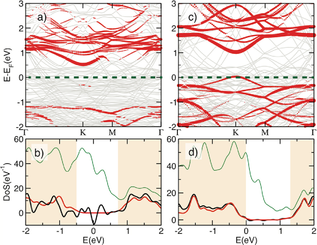
As an example, figure 3(a) gives the band structure of the Pt(111)/MoTe2 interface. The direct interaction between MoTe2 and the Pt surface perturbs the band structure of MoTe2 significantly, the valence bands in particular. The perturbation is accompanied by the formation of IGS inside the MoTe2 band gap, figure 3(b), which pin the Fermi level. The SB height is defined as
| (1) |
with the Fermi energy, and the energy of the top of the valence band (measured as distances, i.e., positive numbers, from the vacuum level). The SB to an electronically perturbed overlayer is of course not extremely well-defined. One can estimate the SB by aligning the core levels of the adsorbed MoTe2 layer to those of a free-standing MoTe2 layer, which gives eV. With eV (figure 1) this gives eV as the work function of of Pt covered by a MoTe2 monolayer. As the calculated work function of clean Pt(111) is 5.91 eV, it implies that adsorbing MoTe2 on Pt creates a large potential step at the interface of 1.36 eV.
The changes in the electronic structure of the adsorbed MoTe2 layer are visualized in figure 3(b). Starting from the total density of states (DoS) of the Pt(111)/MoTe2 system, and subtracting the DoS of the clean Pt(111) slab, one can compare the result to the DoS of a free-standing MoTe2 layer. The comparison shows considerable differences in the MoTe2 band gap region, which are direct evidence for the formation of IGS.
The pattern of these IGS depends on the particular metal/MX2 combination. We have however not found an elemental high work function metal that does not give IGS. For all high work function metal/MX2 contacts we have studied, IGS are formed that pin the Fermi level and yield a sizable SB. The same problem has emerged previously for low work function metals and n-type SBs. Introducing a buffer layer can break the interaction between MX2 and the metal and eliminate the IGS. This layer must be sufficiently thin, such that it does not form a large barrier for the charge carriers. In addition, the interaction between MX2 and the buffer layer must not create new IGS.
A single atomic layer of graphene or h-BN obeys these criteria. Such a layer presents only a thin barrier that essentially allows for metallic transport through the layer.33 Inserting graphene or a h-BN monolayer between a metal surface and MX2 disrupts the metal-MX2 chemical interaction, and destroys any metal-induced IGS. Graphene or h-BN bind to MX2 via van der Waals forces. One does not expect such an interaction to create new IGS. This is illustrated for Pt(111)/h-BN/MoTe2 in figures 3(c) and (d). Inserting a monolayer of h-BN restores the electronic structure of WTe2, where the projected bands are essentially those of free-standing MoTe2. The DoS of Pt(111)/h-BN/MoTe2 minus that of Pt(111) is essentially identical to the DoS of a free-standing MoTe2 layer, in particular in the gap region. In other words, it shows no sign of IGS generated by any h-BN/MoTe2 interaction.
The concept also works if one uses graphene to cover the metal. The interaction between metal/graphene or metal/h-BN and MX2 is van der Waals, so the electronic structure of any MX2 is preserved, and IGS are absent. A serious drawback however is that adsorption of graphene or h-BN generally decreases the metal work function considerably, e.g., by 0.6-1.1 eV for Pt and Au, see table 1. The reduction originates from a dipole layer that is formed at the metal/graphene or metal/h-BN interface, where Pauli exchange repulsion gives an dominant contribution.34
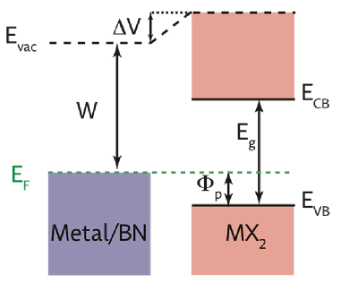
The reduction is partly canceled by a potential step formed at the graphene/MX2 or h-BN/MX2 interface, see figure 4. Although the weak interaction between h-BN and MX2 does not give IGS, it does lead to an interface potential step, which originates from the Pauli repulsion between the electrons from the h-BN layer and those originating from the MX2 layer.34 As the chalcogenide atoms form the outer atomic layers in MX2, it is then not surprising that depends on the chalcogenide species, but not on the metal species of the central atomic layer, see table 1. For graphene/MX2 and h-BN/MX2 interfaces is positive toward MX2 i.e., it decrease the SB. The steps are actually quite moderate, i.e. in the range 0.2-0.3 eV, see table 1, so they do not cancel out the work function reductions discussed in the previous paragraph.
| MoSe2 | WSe2 | MoTe2 | WTe2 | ||||||
|---|---|---|---|---|---|---|---|---|---|
| Pt/Gr | 4.86 | 0.21 | 0.42 | 0.21 | 0.21 | 0.28 | 0 | 0.28 | 0 |
| Pt/h-BN | 5.00 | 0.18 | 0.31 | 0.18 | 0.10 | 0.24 | 0 | 0.24 | 0 |
| Pt/MoS2 | 5.32 | 0.14 | 0.03 | 0.14 | 0 | 0.18 | 0 | 0.18 | 0 |
| Au/Gr | 4.80 | 0.21 | 0.48 | 0.21 | 0.27 | 0.28 | 0 | 0.28 | 0 |
| Au/h-BN | 4.88 | 0.18 | 0.43 | 0.18 | 0.22 | 0.24 | 0 | 0.24 | 0 |
| Au/MoS2 | 5.05 | 0.14 | 0.30 | 0.14 | 0.09 | 0.18 | 0 | 0.18 | 0 |
One obtains a zero SB height only with graphene- or h-BN-covered metals with a high work function, such as Pt and Au, in contact with MX2 that has a sufficiently low ionization potential. The SB height can be calculated from the numbers given in table 1 and figure 1
| (2) |
As by definition , a negative number indicates a zero SB height, . Only the tellurides MoTe2 and WTe2 satisfy this criterion. WSe2 gives a small SB of 0.10 eV with Pt/h-BN but the other selenide monolayers give appreciable SB heights in the range 0.2-0.5 eV. The sulfides (not shown in table 1) have large SBs with heights eV.
One can however expect that the situation becomes more favorable for MX2 multilayers as the band gap of multilayer MX2 is smaller than that of a MX2 monolayer. For MoS2 it has been argued that the band gap reduction is monotonic in the number of layers and that it is equally divided into an upward shift of the valence band and a downward shift of the conduction band.35 This is likely to hold more generally for all MX2 compounds. Indeed an explicit calculation of bilayer WSe2 on Pt/h-BN gives a SB that is zero. It implies that vanishing SBs to multilayer WSe2 are possible with graphene- or h-BN-covered high work function metals.
Adding additional h-BN layers on top of a h-BN/Au or h-BN/Pt substrate does not change the SB height, as the potential steps formed at the interfaces between the h-BN layers are negigibly small. By itself h-BN is an insulator forming SBs for holes with heights 0.9-1.1 eV and 1.1-1.3 eV with Pt and Au, respectively.28 Therefore, h-BN acts as a tunnel barrier between Pt or Au and MX2. A single h-BN layer forms only a thin barrier that is very transparent,33 but the contact resistance is expected to grow exponentionally with the number of h-BN layers.36
The principles outlined above can be extended to other buffer layers besides graphene or h-BN. For instance, adsorbing a single MoS2 layer on a high work function metal such as Au or Pt reduces its work function by 0.5-0.7 eV. That still leaves us with a substrate that has a sufficiently high work function to yield p-type contacts to the tellurides with a zero SB height, and a small to zero SB height to the selenides, see table 1. As the Fermi level for MoS2 adsorbed on Au or Pt is close to the middle of the MoS2 band gap,21 the MoS2 layer then acts as tunnel barrier between the metal and the MX2 layer. Because a MoS2 monolayer is thicker than graphene or h-BN, one expects it to present more of a barrier, and yield a higher contact resistance.
2.2 High electron affinity oxide layers
A buffer layer that effectively decreases a metal work function limits the scope for using it to create p-type contacts. A buffer layer that increases the work function would be more advantageous, which requires a layer that accepts electrons from the underlying metal. Oxides such as MoO3 and WO3 are known for their potential as p-type contacts in organic photovoltaics and light-emitting diodes,16, 17 and have also been tested in field-effect transistors based upn MX2.18, 19 More specifically, -MoO3 (the thermodynamically stable phase of MoO3) is a layered material, which consists of covalently bonded bilayers, see figure 1, that are van der Waals stacked. MoO3 is a large band gap material with an experimental band gap of 3.0 eV. The electron affinity of this material is however an exceptionally high 6.7-6.9 eV.16, 17 Therefore, MoO3 is predicted to be an electron acceptor with respect to common metals.
Adsorbing a MoO3-bilayer on a common metal leads to a transfer of electrons from the metal to the MoO3, and sets up a dipole layer that effectively increases the work function, provided that the adsorption process does not destroy the structure and integrity of the MoO3 overlayer. For instance, the calculated electron work function of Cu(111)/bilayer-MoO3 is 7.08 eV, as compared to 4.98 eV for the clean Cu(111) surface. Moreover, the density of states of the MoO3 conduction band is sufficiently high such as to pin the Fermi level at the bottom of the conduction band, see figure 5.
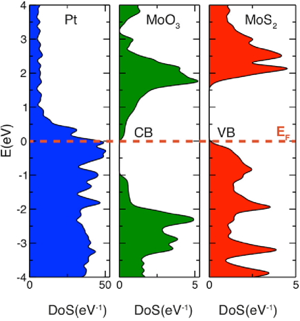
A MoO3 bilayer has no dangling bonds. A MX2 layer adsorbed on MoO3 is therefore likely to be van der Waals-bonded. Indeed from our calculations we find a small MoO3-MoS2 equilibrium binding energy of eV per MoS2 formula unit, and a large equilibrium bonding distance (between to top layer of oxygen atoms and the bottom layer of sulfur atoms) of 3.1 Å. The weak MoS2/MoO3 bonding has little influence on the electronic structure of either layer. Any metal that can be covered by bilayer-MoO3 without disrupting its structure should then give a work function that is sufficiently high to give a zero SB height to all MX2, see figure 2. As electrons are transferred from MX2 to MoO3, thereby pinning the Fermi level at the top of the MX2 valence band, as well as at the bottom of the MoO3 conduction band, see figure 5.
The MoO3 layer does not act as a tunnel barrier, as transport of charge carriers takes place through the conduction band of the oxide. If one adds additional MoO3 layers, one expects that for thicknesses below the mean free path of the charge carriers the characteristics for injection from the metal into the MX2 layer remain the same. The contact resistance does increase for thicker MoO3 layers, however, as charge carrier mobilities in oxide layers are typically substantially smaller than in metals.18
In principle any oxide that has a layered structure can be used this way. One can cover a metal with an oxide monolayer; if the oxide layer bonds to MX2 through van der Waals interactions, and if its electron affinity is sufficiently high, it should give a p-type contact. In contrast to graphene or h-BN, the metal species is not very important, as the conduction band of the oxide pins the Fermi level. Besides MoO3, for instance V2O5 has a layered structure and a high electron affinity of up to 7 eV.16 A drawback of using such oxide layers are that they are strong oxidizing agents, which can react with molecules in the environment, or with the metal electrodes. For instance, the Cu/MoO3 interface is metastable and oxidized Cu ions can diffuse into MoO3.16 Other metal/MoO3 interfaces, such as Au/MoO3, are stable, however.
2.3 Metallic buffer layers
A buffer with a high electron affinity that is less reactive than an oxide would be very convenient. Metallic , , compounds have a layered hexagonal structure similar to that of semiconducting MX2. The latter compounds contain a group VI transition metal M, whereas the former compounds contain a group V transition metal . The electronic structure of these two compound groups is basically similar, but in MX2 the topmost valence band is completely filled, whereas in it is only half-filled because has one electron less than M.31 This makes the compounds metallic with a relatively high work function. For example, NbS2 and TaS2 monolayers have calculated work functions of 6.22 and 6.12, respectively.
Most common metals have a lower work function. If they are covered by a monolayer, electrons are transferred from the metal to the layer, effectively increasing the work function, as in the case of an MoO3 overlayer. As the density of states at the Fermi level of is high, the transferred electrons will hardly modify the Fermi level, which is therefore effectively pinned by the layer. For instance, the Au(111) and Al(111) surfaces have calculated work functions of 5.43 and 4.24 eV, respectively. Adsorbing a NbS2 monolayer gives work functions of Au/NbS2 and Al/NbS2 surfaces of 6.11 and 6.06 eV, respectively. In other words, the work function differs by eV from that of a free-standing NbS2 monolayer, irrespective of the metal substrate.
This remarkable property make metallic compounds viable buffer layers for making p-doped contacts to MX2 semiconductors. We envision that layers can be deposited on a metal substrate in a similar way as MX2 layers. A MX2 layer can then be deposited on by van der Waals epitaxy, for instance.6, 7 The interaction at the /MX2 interface is van der Waals, which hardly perturbs the electronic structure of either layer. The potential step at the /MX2 interface, eV, is small and hardly affects the work function.
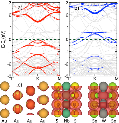
Figure 6 shows the calculated band structure of the Au(111)/NbS2/WSe2 multilayer. It illustrates the perfect p-type contact formed in this case, with the Fermi level coinciding with the top of the WSe2 valence band. At the same time the Fermi cuts the valence band of NbS2, confirming that it acts as a conducting layer. Indeed, the local DoS calculated at the Fermi energy shows a state that is delocalized over the whole multilayer, see figure 6. We expect that similar p-type contacts can be formed with other MX2 layers using NbS2 or TaS2 monolayers as a buffer.
Adding additional NbS2 or TaS2 layers, the charge carrier injection into MX2 should remain the same as long as the thickness of the buffer layers is below the mean free path of the charge carriers. For thicker layers the contact resistance starts to depend on the thickness of the buffer layers.
3 Conclusions
We propose a particular technique to construct p-type contacts with zero SB heights to MX2 (M = Mo,W; X = S,Se,Te) 2D semiconductors. Using first-principles DFT calculations we show that a direct metal/MX2 interaction leads to interface states that pin the Fermi level in the MX2 band gap, giving a sizable SB. Inserting a well-chosen buffer layer between the metal surface and the MX2 layer breaks this interaction, and unpins the Fermi level, if MX2 is bonded to the buffer layer with van der Waals forces.
A monolayer of h-BN or graphene constitute only a thin barrier for transport. Adsorbing h-BN on a high work function metal such as Pt or Au, gives a zero SB height for contacts to the MX2 tellurides, a low SB to WSe2, and zero SB heights for contacts to telluride and selenide multilayers. Adsorbing graphene works in a similar way, but is somewhat less effective in reducing SBs. To obtain p-type contacts one has to combine these layers with high work function metals, as adsorption of h-BN or graphene substantially reduces the work function of the metal substrate.
Alternatively one can use a buffer layer of an oxide with a high electron affinity. By explit calculations on metal/MoO3 we show that adsorbing a bilayer of MoO3 gives a zero SB height for contacts to all MX2. The metal substrate is relatively unimportant here, as the Fermi level is pinned at the MoO3 conduction band, which also ensures that bilayer-MoO3 does not act as a tunnel barrier to MX2. Bilayer-MoO3 binds to MX2 layers via van der Waals interactions, consistent with the principal idea of this paper.
Strong oxididants such as MoO3 might suffer from chemical instability. The most elegant solution for the p-type contact problem is using a metallic (M = Nb,Ta; X = S) monolayer as a buffer. These compounds are stable and have a high work function. Adsorbed on a metal substrate they yield a high work function contact, which gives a zero SB height to all MX2 monolayers. The metal substrate is of little importance, as the Fermi level is pinned by the layer. MX2 forms a van der Waals bonded contact to , and the states formed at the Fermi level extend throughout the whole metal//MX2 multilayer.
4 Computational section
We perform first-principles density functional theory (DFT) calculations using the VASP code and the projector augmented wave (PAW) datasets from the VASP database.37, 38, 39, 40 For the computational set-up and the choice of computational parameters (unit cell, -point sampling, etc.) we follow Refs. 21 and 41.
Obviously different 2D materials have different in-plane lattice constants. Van der Waals stacking of 2D materials then generally leads to incommensurable structures, which are observed experimentally in the form of moiré patterns. In electronic structure calculations one is forced to approximate these by commensurable structures, which introduces an artificial strain. As the MX2 electronic structure is very sensitive to strain, we keep the in-plane lattice constant of MX2 at its optimized value, adapting the lattice constant of the metal surfaces and the buffer layers accordingly. The supercells defining the commensurable structures are constructed such that the lattice mismatches between the different layers are minimal, following the technique explained in Ref. 41. As an example, a (22) MoTe2 cell on top of (33) h-BN on () Pt gives lattice mismatches of 6 and 4% in the h-BN and Pt lattices respectively.
Van der Waals interactions are vital to descibe the bonding between the layers. Here we use the van der Waals density functional opt86b-vdW-DF.51, 52, 53 The optimized lattice parameters of MX2 monolayers are in good agreement with the experimental lattice parameters of the bulk hexagonal structures, see table 2. (The experimental structure of WTe2 is not hexagonal;54 it has been added for completeness reasons.) Also in table 2 are listed the calculated monolayer band gaps . DFT calculations usually severely underestimate band gaps, but for MX2 monolayers the differences are tolerable, if one compares to the measured optical gaps of the monolayers, see table 2.
Such a comparison is not entirely fair, as is the exciton binding energy. The latter depends strongly on the environment of the exciton, and decreases if the electrodynamic screening by the environment increases.55 Values of the exciton binding energy between zero,46, 56 and 0.5 eV45, 48 have been reported. In our case one expects the screening to be strong as the MX2 layers are close to a metal substrate, and we speculate the exciton binding energy to be relatively small.
Comparing to previous calculations, one observes that the opt86b-vdw-DF functional gives an improvement over the GGA/PBE functional regarding optimized lattice constants and band gaps of MX2.57 The opt86b-vdw-DF lattice constants are close to the HSE06 values, and the band gaps are in between the GGA/PBE and HSE06 values. Concerning the absolute positions of the energy levels, the valence band maxima calculated with opt86b-vdw-DF (figure 1) and HSE0657 are generally with eV of one another. It is difficult to compare these values to experimental data. Note however that the experimentally determined valence band offset of 0.83 eV between MoS2 and WSe2,45 is in excellent agreement with the 0.83 eV derived from the numbers in figure 1.
5 Acknowledgment
This work is part of the research program of the Foundation for Fundamental Research on Matter (FOM), which is part of the Netherlands Organisation for Scientific Research (NWO). The use of supercomputer facilities was sponsored by the Physical Sciences Division (EW) of NWO.
References
- Chhowalla et al. 2013 Chhowalla, M.; Shin, H. S.; Eda, G.; Li, L.-J.; Loh, K. P.; Zhang, H. Nature Chemistry 2013, 5, 263Ð275
- Cui et al. 2015 Cui, Y. et al. Adv. Mater. 2015, 27, 5230–5234
- Wang et al. 2012 Wang, Q. H.; Kalantar-Zadeh, K.; Kis, A.; Coleman, J. N.; Strano, M. S. Nat. Nanotechnol. 2012, 7, 699–712
- Zhang et al. 2013 Zhang, W.; Huang, J.-K.; Chen, C.-H.; Chang, Y.-H.; Cheng, Y.-J.; Li, L.-J. Adv. Mater. 2013, 25, 3456–3461
- Geim and Grigorieva 2013 Geim, A. K.; Grigorieva, I. V. Nature 2013, 499, 419–425
- Lee et al. 2012 Lee, Y.-H.; Zhang, X.-Q.; Zhang, W.; Chang, M.-T.; Lin, C.-T.; Chang, K.-D.; Yu, Y.-C.; Wang, J. T.-W.; Chang, C.-S.; Li, L.-J.; Lin, T.-W. Adv. Mater. 2012, 24, 2320–2325
- Chen et al. 2015 Chen, J.; Liu, B.; Liu, Y.; Tang, W.; Nai, C. T.; Li, L.; Zheng, J.; Gao, L.; Zheng, Y.; Shin, H. S.; Jeong, H. Y.; Loh, K. P. Adv. Mater. 2015, 27, 6722–6727
- George et al. 2014 George, A. S.; Mutlu, Z.; Ionescu, R.; Wu, R. J.; Jeong, J. S.; Bay, H. H.; Chai, Y.; Mkhoyan, K. A.; Ozkan, M.; Ozkan, C. S. Adv. Func. Mater. 2014, 24, 7461–7466
- Fang et al. 2012 Fang, H.; Chuang, S.; Chang, T. C.; Takei, K.; Takahashi, T.; Javey, A. Nano Lett. 2012, 12, 3788–3792
- Shokouh et al. 2015 Shokouh, S. H. H.; Jeon, P. J.; Pezeshki, A.; Choi, K.; Lee, H. S.; Kim, J. S.; Park, E. Y.; Im, S. Adv. Func. Mater. 2015, 10.1002/adfm.201502008
- Joonki et al. 2014 Joonki, S.; Tae-Eon, P.; Der-Yuh, L.; Deyi, F.; Joonsuk, P.; Hee, J. J.; Yabin, C.; Changhyun, K.; Chaun, J.; Yinghui, S.; Robert, S.; Joonyeon, C.; Sefaattin, T.; Junqiao, W. Nano Lett. 2014, 14, 6976–6982
- Kang et al. 2015 Kang, D.-H.; Kim, M.-S.; Shim, J.; Jeon, J.; Park, H.-Y.; Jung, W.-S.; Yu, H.-Y.; Pang, C.-H.; Lee, S.; Park, J.-H. Adv. Func. Mater. 2015, 25, 4219–4227
- Çakır et al. 2014 Çakır, D.; Sevik, C.; Peeters, F. M. J. Mater. Chem. C 2014, 2, 9842–9849
- Allain and Kis 2014 Allain, A.; Kis, A. ACS Nano 2014, 8, 7180–7185
- Braga et al. 2012 Braga, D.; Lezama, I. G.; Berger, H.; Morpurgo, A. F. Nano Lett. 2012, 12, 5218–5223
- Greiner et al. 2013 Greiner, M. T.; Chai, L.; Helander, M. G.; Tang, W.-M.; Lu, Z.-H. Adv. Func. Mater. 2013, 23, 215–226
- Kröger et al. 2009 Kröger, M.; Hamwi, S.; Meyer, J.; Riedl, T.; Kowalsky, W.; Kahn, A. Appl. Phys. Lett. 2009, 95, 123301
- Chuang et al. 2014 Chuang, S.; Battaglia, C.; Azcatl, A.; McDonnell, S.; Kang, J. S.; Yin, X.; Tosun, M.; Kapadia, R.; Fang, H.; Wallace, R. M.; Javey, A. Nano Lett. 2014, 14, 1337–1342
- McDonnell et al. 2014 McDonnell, S.; Addou, R.; Buie, C.; Wallace, R. M.; Hinkle, C. L. ACS Nano 2014, 8, 2880–2888
- Chen et al. 2013 Chen, W.; Santos, E. J. G.; Zhu, W.; Kaxiras, E.; Zhang, Z. Nano Lett. 2013, 13, 509–514
- Farmanbar and Brocks 2015 Farmanbar, M.; Brocks, G. Phys. Rev. B 2015, 91, 161304
- Gong et al. 2014 Gong, C.; Colombo, L.; Wallace, R. M.; Cho, K. Nano Lett. 2014, 14, 1714–1720
- Kang et al. 2014 Kang, J.; Liu, W.; Sarkar, D.; Jena, D.; Banerjee, K. Phys. Rev. X 2014, 4, 031005
- Kappera et al. 2014 Kappera, R.; Voiry, D.; Yalcin, S. E.; Branch, B.; Gupta, G.; Mohite, A. D.; Chhowalla, M. Nat. Mat. 2014, 13, 1128–1134
- Momma and Izumi 2008 Momma, K.; Izumi, F. J. Appl. Cryst. 2008, 41, 653–658
- Giovannetti et al. 2008 Giovannetti, G.; Khomyakov, P. A.; Brocks, G.; Karpan, V. M.; van den Brink, J.; Kelly, P. J. Phys. Rev. Lett. 2008, 101, 026803
- Khomyakov et al. 2009 Khomyakov, P. A.; Giovannetti, G.; Rusu, P. C.; Brocks, G.; van den Brink, J.; Kelly, P. J. Phys. Rev. B 2009, 79, 195425
- Bokdam et al. 2014 Bokdam, M.; Brocks, G.; Katsnelson, M. I.; Kelly, P. J. Phys. Rev. B 2014, 90, 085415
- Chuang et al. 2014 Chuang, H.-J.; Tan, X.; Ghimire, N. J.; Perera, M. M.; Chamlagain, B.; Cheng, M. M.-C.; Yan, J.; Mandrus, D.; Tomànek, D.; Zhou, Z. Nano Lett. 2014, 14, 3594–3601
- Leong et al. 2015 Leong, W. S.; Luo, X.; Li, Y.; Khoo, K. H.; Quek, S. Y.; Thong, J. T. L. ACS Nano 2015, 9, 869–877
- Mattheiss 1973 Mattheiss, L. F. Phys. Rev. B 1973, 8, 3719–3740
- Lince et al. 1987 Lince, J. R.; Carré, D. J.; Fleischauer, P. D. Phys. Rev. B 1987, 36, 1647–1656
- Yazyev and Pasquarello 2009 Yazyev, O.; Pasquarello, A. Phys. Rev. B 2009, 80, 035408
- Bokdam et al. 2014 Bokdam, M.; Brocks, G.; Kelly, P. J. Phys. Rev. B 2014, 90, 201411
- Li et al. 2014 Li, S.-L.; Komatsu, K.; Nakaharai, S.; Lin, Y.-F.; Yamamoto, M.; Duan, X.; Tsukagoshi, K. ACS Nano 2014, 8, 12836–12842
- Britnell et al. 2012 Britnell, L.; Gorbachev, R. V.; Jalil, R.; Belle, B. D.; Schedin, F.; Katsnelson, M. I.; Eaves, L.; Morozov, S. V.; Mayorov, A. S.; Peres, N. M. R.; Neto, A. H. C.; Leist, J.; Geim, A. K.; Ponomarenko, L. A.; Novoselov, K. S. Nano Lett. 2012, 12, 1707–1710
- Kresse and Hafner 1993 Kresse, G.; Hafner, J. Phys. Rev. B 1993, 47, 558–561
- Kresse and Furthmüller 1996 Kresse, G.; Furthmüller, J. Phys. Rev. B 1996, 54, 11169–11186
- Blöchl 1994 Blöchl, P. E. Phys. Rev. B 1994, 50, 17953–17979
- Kresse and Joubert 1999 Kresse, G.; Joubert, D. Phys. Rev. B 1999, 59, 1758–1775
- Farmanbar and Brocks 2015 Farmanbar, M.; Brocks, G. arXiv:1510.04337v2 2015,
- Böker et al. 2001 Böker, T.; Severin, R.; Müller, A.; Janowitz, C.; Manzke, R.; Voß, D.; Krüger, P.; Mazur, A.; Pollmann, J. Phys. Rev. B 2001, 64, 235305
- Schutte et al. 1987 Schutte, W.; Boer, J. D.; Jellinek, F. J. Solid State Chem. 1987, 70, 207 – 209
- Ohno 1998 Ohno, Y. Phys. Rev. B 1998, 58, 8042–8049
- Chiu et al. 2015 Chiu, M.-H.; Zhang, C.; Shiu, H.-W.; Chuu, C.-P.; Chen, C.-H.; Chang, C.-Y. S.; Chen, C.-H.; Chou, M.-Y.; Shih, C.-K.; Li, L.-J. Nat. Commun. 2015, 6, 7666
- Mak et al. 2010 Mak, K. F.; Lee, C.; Hone, J.; Shan, J.; Heinz, T. F. Phys. Rev. Lett. 2010, 105, 136805
- Tongay et al. 2012 Tongay, S.; Zhou, J.; Ataca, C.; Lo, K.; Matthews, T. S.; Li, J.; Grossman, J. C.; Wu, J. Nano Lett. 2012, 12, 5576–5580
- Ugeda et al. 2014 Ugeda, M. M.; Bradley, A. J.; Shi, S.-F.; da Jornada, F. H.; Zhang, Y.; Qiu, D. Y.; Ruan, W.; Mo, S.-K.; Hussain, Z.; Shen, Z.-X.; Wang, F.; Louie, S. G.; Crommie, M. F. Nat. mater. 2014, 13, 1091
- Ruppert et al. 2014 Ruppert, C.; Aslan, O. B.; Heinz, T. F. Nano Lett. 2014, 14, 6231–6236
- Gutiérrez et al. 2013 Gutiérrez, H. R.; Perea-López, N.; Elías, A. L.; Berkdemir, A.; Wang, B.; Lv, R.; López-Urías, F.; Crespi, V. H.; Terrones, H.; Terrones, M. Nano Lett. 2013, 13, 3447–3454
- Dion et al. 2004 Dion, M.; Rydberg, H.; Schröder, E.; Langreth, D. C.; Lundqvist, B. I. Phys. Rev. Lett. 2004, 92, 246401
- Klimeš et al. 2011 Klimeš, J.; Bowler, D. R.; Michaelides, A. Phys. Rev. B 2011, 83, 195131
- Thonhauser et al. 2007 Thonhauser, T.; Cooper, V. R.; Li, S.; Puzder, A.; Hyldgaard, P.; Langreth, D. C. Phys. Rev. B 2007, 76, 125112
- Dawson and Bullett 1987 Dawson, W. G.; Bullett, D. W. J. Phys. C: Solid State Phys. 1987, 20, 6159
- van der Horst et al. 1999 van der Horst, J.-W.; Bobbert, P. A.; Michels, M. A. J.; Brocks, G.; Kelly, P. J. Phys. Rev. Lett. 1999, 83, 4413–4416
- Zhang et al. 2014 Zhang, Y. et al. Nat. Nanotechnol. 2014, 9, 111
- Kang et al. 2013 Kang, J.; Tongay, S.; Zhou, J.; Li, J.; Wu, J. Appl. Phys. Lett. 2013, 102, 012111