Now at ]ABB Corporate Research Center, Switzerland
The relation between optical instabilities and absorbed material in photoluminescence with [0001] InGaN single quantum well.
Abstract
In this letter, we aim to elucidate the physical mechanism of the so called optical memory effect and blinking phenomenon observed in InGaN single quantum wells (SQW). We have found that the optical response of both memory effect and blinking phenomenon, is affected by different excitation wavelengths and by the change of gas adsorption on the crystal surface. A model that reproduce dynamics of the coverage of absorbed gas molecules on the sample surface is given and compared with experimental data with evident match.
pacs:
Valid PACS appear hereInGaN-based LED of green-ultraviolet region and white LED with phosphor have come into practical use. However, the crystal growth methods and understanding of InGaN devices are still affected by the lack of knowledge about the theoretical background on different phenomenaStrite and Morkoç (1992). For instance, despite the large concentration of threading dislocations ()Shikanai et al. (1997); Kaneta et al. (2006) due to lattice mismatchZheleva et al. (1997), InGaN optical devices achieve very high internal quantum efficiency and optical emission. In addition, InGaN quantum wells with high Indium composition domains, such as quantum dots (QDs), are known to induce local excitation emission (bright spots/points)Micheletto et al. (2004); Narukawa and Kawakami (1997).
Recently, instability blinkingOikawa et al. (2011); Micheletto et al. (2006) and optical memory effectFeldmeier et al. (2009)], observed by PL in InGaN Single Quantum Well (SQW), were reported and associated to the presence of defects and strain within the crystalChichibu et al. (1996).
Instability blinking was found in CdSe nanocrystalNirmal et al. (1996); Yoshikawa et al. (2007) and epitaxial grown filmSeufert et al. (2001); Kaufmann (2013), ZnCdSe quantum dots (QD)Zhang et al. (1998); Soto Rodriguez et al. (2013), GaAs QDBertram et al. (1999); Lyons et al. (2010), InP QDKuno et al. (2001); Sugisaki et al. (2002); Duan and Stampfl (2009) and Porous silicon. In InGaN SQW, instability blinking arises around a QD in a region of few m of diameter and the flashing intensity width is temperature dependentJanotti and Van de
Walle (2008). Therefore, the phenomenon was associated to beating of slightly different thermal wave vibration creating unstable optical blinkingMicheletto et al. (2013).
On the other side, the so called “optical memory effect” was first found in the GaN epitaxial filmFeldmeier et al. (2009); Van de Walle and Neugebauer (2004). Optical memory effect in InGaN is the phenomenon in which photoluminescence emission becomes gradually stronger on a time scale of seconds to few minutes and depends from the previous illumination history of the sample (hence the name optical memory effect).
A complete and universally accepted theory to explain these two phenomena is unknown.
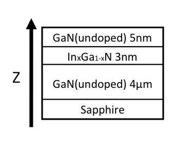
In this study, we employed InGaN SQW grown in (0001) direction with the MOVPE method (fig. 1).
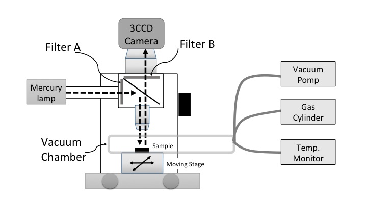
The InGaN SQW layers are composed of an undoped GaN layer (4 ) on a sapphire substrate, an InGaN active layer (3nm), and an undoped GaN layer (5nm). The main peak of the bulk macroscopic photoluminescence was about 540nm. The SQW was optically characterized by the experimental setup shown in Fig. 2.
The sample in placed in a vacuum chamber (RC102-CFM, CIA, Inc.), connected to a turbo-molecular vacuum pump (TSH 071 E, Pfeiffer), to a temperature controller (Model 32, Cryogenic Control Systems, Inc.) and a gas cylinder.
The dynamics of the photoluminescence is detected by using a selective excitation fluorescence microscope (BX51WX, Olympus) coupled with a CCD camera (HDR-SR1, SONY). The time variation of the light emission surface is recorded as video data at 60 frames/second. Ultraviolet Hg lamp was used as excitation light (365nm and 405nm emission lines). The 365nm light excites both of InGaN layer and GaN layers. On the other hand, 405nm light excites only the InGaN layer.
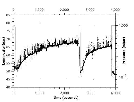
In Fig. 3, we show the effects of air pressure (from 1000 mbar down to mbar) on the photoluminescence. It can be seen that there is a variation of the overall emission intensity when changing the degree of vacuum. The gray curve represent the change of pressure in log scale, whereas the dots are the sample luminosity, averaged on the entire surface. The sample is excited by a 365 nm signal.
We see that whole emission intensity varies dynamically depending on pressure. In high vacuum, the emission improves and grows to a pleteau 40 higher than the baseline at one atmosphere. Also, the luminosity distribution becomes homogeneous. On the contrary, at air pressure, the intensity drops to lower values and the emission spatial distribution is less uniform with many bright points, some of those result to be blinking.
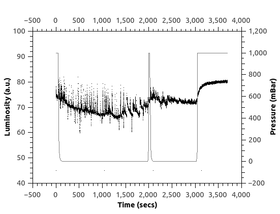
On the other hand, excitating the sample at 405nm we observe small changes of intensity in response to pressure, the PL emission on the surface is homogeneous and we observe no blinking points (figure 4). Since with 405 nm we do not excite the InGaN layer, this suggests that the blinking and those Intense Luminous Centers are associated with the GaN/InGaN interface in proximity of the surface.
To understand the physical mechanism that drives this effect, we have to consider that, in general, adsorption by Van der Waals’ forces on the surface of a material changes with the degree of vacuum. In addition, the presence of blinking points and overall emission intensity depends on pressure, suggesting that the phenomenom is driven by a change in the amount of adsorbed species on the surface.
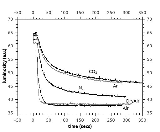
In order to prove this, we proceeded by creating vacuum in a room temperature vacuum chamber (about 300 K and mbar) and then by injecting gas, like air, pure dry air (O2 : N2 = 2 : 8), N2 gas, Ar gas, and CO2 into the chamber, reaching up to a pressure of 1000 mbar (1 atm). Following the injection of each gas, we observed the variation of PL emission. Since there are almost no optical emission variations when InGaN SQW is excited with 405nm wavelength, in the following experiments we will only used 365nm excitation light.
In Fig. 5 it is shown the PL profile when a sample excited by 365nm wavelength is brought back from high vacuum condition to 1000 mbar for each injected gas. It can be seen that air and pure dry air greatly reduce the PL emission. On the other hand, Ar and CO2 gas have a low impact, whereas N2 gas have an intermediate effect. Based on this evidence, we put forward the hypothesis that molecular oxygen is the most effective specie and the main cause of emission variation.
This is in accordance with what reported by both Zywietz et al (Staszszak et al., 2013), who showed that GaN surface is very active towards oxygen incorporation, and by Pearon et al. Pearton et al. (1999), who experimentally demonstrated that oxygen can be found in GaN up to a depth of 180 nm. More recently, density functional theory calculations revealed that oxygen can be easily incorporated into InGaN mono-layer QW (MLQW) Alfieri et al. (2015) in accordance with the experimental results of Kappers et al. Kappers et al. (2015) who reported that growing N-poor InGaN leads to high levels of oxygen incorporation. The detrimental effects of oxygen in InGaN are known: it can compensate dopants, making the growth of p-type InGaN difficultMiao et al. (2013) and it has been held responsible for the degradation of InGaN/GaN LEDMoses et al. (2011); Yang et al. (2011); Okada et al. (2014).
We model the relation between emission intensity and ambient pressure in order to give an explanation for the decreased emission at higher pressure. We base ourselves on a simple molecular coverage dynamics theory. We suppose that the optical emission, generated at the InGan/GaN interface, is decreased by the presence of absorbed molecules on the surface accordingly to this linear relation:
| (1) |
where is an offset, a coefficient and the number of molecules present on the surface at time . The term represents the maximum luminosity the sample can have if there are no molecules on the surface.
To model how varies in time, we consider a space where molecules can be absorbed or desorbed as an uni-dimensional line representing the surface of the sample. For simplicity hereafter we call it ”surface” and the rate of change of can be expressed as follows:
| (2) |
the first term represents the molecules that leave the surface per unity of time. The parameter is the probability that each of the molecules is desorbed and it is a function of time, as we will see below.
The other addendum represents the rate of absorption, that is, in the same fashion, given by the product of a probability and a number of particles. We define as the number of particles that realize a complete coverage on the surface, thus represents how much space is available on the surface for absorption, measured in particle units. The probability to have a random gas particle landing on the surface is proportional to this space.
As mentioned above, these probabilities and may not be constant, but depend on, for example, time variable gas pressure, accordingly to a linear relation:
| (3) | |||||
where and are two offsets that represent the range of pressure and is the coefficient that fit the experimental data. In the differential equation (2), the first term on the right is clearly an exponential decay, whereas the second shows a logistic nature, so the three equations (1), (2) and (The relation between optical instabilities and absorbed material in photoluminescence with [0001] InGaN single quantum well.) altogether result in an exponential growth or exponential decay behavior, depending on the pressure parameter.
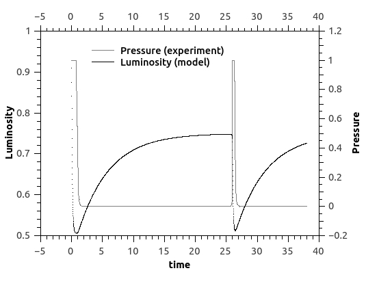
If we integrate numerically the differential equation (2) and run a simulation with the experimental variable pressure data inserted in equation (The relation between optical instabilities and absorbed material in photoluminescence with [0001] InGaN single quantum well.) we obtain the result in figure 6 that is strikingly similar to the behavior found in the experiments suggesting that is a dynamically changing coverage of spurious gas molecules absorbed on the surface that causes the photoluminescence variations observed experimentally.
We found that photoluminescence has lower intensity and shows unevenly distributed intense luminous centersMicheletto et al. (2004) (bright spots) and some blinking points when the level of absorption coverage is high on the sample surface. In contrast, when vacuum is drawn and spurious gas particles are desorbed, sample surface emission has higher intensity and it is homogeneous, with almost no bright spots or blinking points.
We speculate that unstable blinking and the so called optical memory effect are caused by absorbed material on the surface of the sample. In particular, the presence of O2 in the proximity of the surface, induce adsorption that influence the excitation of GaN layers, not not only the InGaN layer.
We developed a working phenomenological model that fits properly the experimental curves that relate the ambient pressure and the sample photoluminescence.
This study wants to contribute to the understanding of fundamental processes involved in the emission phenomena of InGaN materials and to help break ground to improve the efficiency and reliability of next generation nitride semiconductor devices.
Acknowledgements.
This study was partially supported by the Japanese grant KAKEN (project number 24560014) and by the Yokohama City University Sabbatical fund 2015-2016.References
- Strite and Morkoç (1992) S. Strite and H. Morkoç, Journal of Vacuum Science and Technology, B 10, 1237 (1992).
- Shikanai et al. (1997) A. Shikanai, T. Azuhata, T. Sota, S. Chichibu, A. Kuramata, K. Horino, and S. Nakamura, Journal of Applied Physics 81, 417 (1997).
- Kaneta et al. (2006) A. Kaneta, M. Funato, Y. Narukawa, T. Mukai, and Y. Kawakami, physica status solidi (c) 3, 1897 (2006), 74.
- Zheleva et al. (1997) T. S. Zheleva, O. H. Nam, M. D. Bremser, and R. F. Davis, Applied Physics Letters 71, 2472 (1997).
- Micheletto et al. (2004) R. Micheletto, N. Yoshimatsu, A. Kaneta, Y. Kawakami, and S. Fujita, Applied Surface Science 229, 338 (2004).
- Narukawa and Kawakami (1997) Y. Narukawa and Y. Kawakami, Applied Physics Letters 70, 981 (1997).
- Oikawa et al. (2011) K. Oikawa, C. Feldmeier, U. T. Schwarz, Y. Kawakami, and R. Micheletto, Optical Material Express 1, 158 (2011).
- Micheletto et al. (2006) R. Micheletto, M. Abiko, A. Kaneta, Y. Kawakami, Y. Narukawa, and T. Mukai, Applied Physics Letters 88, 061118 (2006).
- Feldmeier et al. (2009) C. Feldmeier, M. Abiko, U. T. Schwarz, Y. Kawakami, and R. Micheletto, Optics Express 17, 22855 (2009).
- Chichibu et al. (1996) S. Chichibu, T. Azuhata, T. Sota, and S. Nakamura, Applied Physics Letters 69, 4188 (1996).
- Nirmal et al. (1996) M. Nirmal, B. Dabbousi, M. Bawendi, J. Macklin, J. Trautman, T. Harris, and L. Brus, Nature 383, 802 (1996).
- Yoshikawa et al. (2007) A. Yoshikawa, S. B. Che, W. Yamaguchi, H. Saito, X. Q. Wang, Y. Ishitani, and E. S. Hwang, Applied Physics Letters 90 (2007).
- Seufert et al. (2001) J. Seufert, M. Obert, R. Weigand, T. Kuemmell, G. Bacher, A. Forchel, K. Leonardi, and D. Hommel, Phys. Status Solidi B 224, 201–205 (2001).
- Kaufmann (2013) N. Kaufmann, Ph.D. thesis, Ecole Polytechnique de Losanne (2013).
- Zhang et al. (1998) B. Zhang, Y. Li, T. Yasuda, W. Wang, Y. Segawa, K. Edamatsu, and T. Itoh, Applied Physics Letters 73, 1266 (1998).
- Soto Rodriguez et al. (2013) P. E. D. Soto Rodriguez, V. J. Gomez, P. Kumar, E. Calleja, and R. Noetzel, Applied Physics Letters 102 (2013), 10.1063/1.4800779.
- Bertram et al. (1999) D. Bertram, M. Hanna, and A. Nozik, Applied Physics Letters 74, 2666 (1999).
- Lyons et al. (2010) J. L. Lyons, A. Janotti, and C. G. Van de Walle, Applied Physics Letters 97 (2010), 10.1063/1.3492841.
- Kuno et al. (2001) M. Kuno, D. Fromm, A. Gallagher, D. Nesbitt, O. Micic, and A. Nozik, Nano Letters 1, 557 (2001).
- Sugisaki et al. (2002) M. Sugisaki, H. Ren, K. Nishi, and Y. Masumoto, Japanese Journal of Applied Physics 41, 958 (2002), 13th International Conference on Indium Phosphide and Related Materials (IPRM), NARA, JAPAN, MAY 14-18, 2001.
- Duan and Stampfl (2009) X. M. Duan and C. Stampfl, Physical Review B 79 (2009), 10.1103/PhysRevB.79.035207.
- Janotti and Van de Walle (2008) A. Janotti and C. G. Van de Walle, Applied Physics Letters 92 (2008), 10.1063/1.2832369.
- Micheletto et al. (2013) R. Micheletto, K. Oikawa, and C. Feldmeier, Applied Physics Letters 103, 17109 (2013).
- Van de Walle and Neugebauer (2004) C. Van de Walle and J. Neugebauer, Journal of Applied Physics 95, 3851 (2004).
- Staszszak et al. (2013) G. Staszszak, I. Gorczyca, T. Suski, X. Wang, N. Christensen, A. Svane, E. Dimakis, and T. Moustakas, Journal of Applied Physics 113, 123101 (2013).
- Pearton et al. (1999) S. Pearton, H. Cho, J. LaRoche, F. Ren, R. Wilson, and J. Lee, Applied Physics Letters 75, 2939 (1999).
- Alfieri et al. (2015) G. Alfieri, T. Tsutsumi, and R. Micheletto, Applied Physics Letters 106 (2015), 10.1063/1.4919787.
- Kappers et al. (2015) M. J. Kappers, T. Zhu, S.-L. Sahonta, C. J. Humphreys, and R. A. Oliver, physica status solidi (c) 12, 403 (2015).
- Miao et al. (2013) M. S. Miao, Q. M. Yan, and C. G. Van de Walle, Applied Physics Letters 102 (2013), 10.1063/1.4794986.
- Moses et al. (2011) P. G. Moses, M. Miao, Q. Yan, and C. G. Van de Walle, Journal of Chemical Physics 134 (2011).
- Yang et al. (2011) C. C. Yang, J. K. Sheu, C. H. Kuo, M. S. Huang, S. J. Tu, F. W. Huang, M. L. Lee, Y.-H. Yeh, X. W. Liang, and W. C. Lai, IEEE Electron Device Letters 32, 536 (2011).
- Okada et al. (2014) N. Okada, K. Tadatomo, K. Yamane, H. Mangyo, Y. Kobayashi, H. Ono, K. Ikenaga, Y. Yano, and K. Matsumoto, Japanese Journal of Applied Physics 53 (2014).
