Single-Mode Optical Waveguides on Native High-Refractive-Index Substrates
High-refractive-index semiconductor optical waveguides form the basis for modern photonic integrated circuits (PICs) , but the conventional methods of achieving optical confinement require a thick lower-refractive-index support layer that impedes large-scale co-integration with electronics. To address this challenge, we present a general architecture for single-mode waveguides that confine light in a high-refractive-index material on a native substrate. Our waveguide consists of a high-aspect-ratio fin of the guiding material surrounded by lower-refractive-index dielectrics and is compatible with standard top-down fabrication techniques. The proposed waveguide geometry removes the need for a buried-oxide-layer in silicon photonics, as well as the InGaAsP layer in InP-based PICs and will allow for photonic integration on emerging material platforms such as diamond and SiC.
PICs are rapidly being developed for high-refractive index materials that allow for tight optical confinement, small on-chip bend radii, and strong light-matter interactions. For example, high-performance PICs in both silicon Reed_08 and InP Coldren_JLT_11 ; Smit_SST_14 platforms are playing an increasingly important role in data applications with the potential to enable exascale computing Rumley_JLT_15 and on-chip core-to-core optical communication Kimerling_MRS_14 . Similarly, wide-band gap semiconductors, such as diamond Aharonovich_NP_11 ; Castelletto_NJP_11 ; Faraon_NP_11 ; Burek_NComm_14 ; Thomas_OpEx_14 ; Mouradian_PRX_15 ; Hausmann_NP_14 ; Latawiec_Optica_15 and SiC Cardenas_OL_15 , have emerged as promising materials for a plethora of new PIC applications. Among these are non-linear optics Hausmann_NP_14 ; Latawiec_Optica_15 ; Cardenas_OL_15 and integrated quantum information processing Faraon_NP_11 ; Burek_NComm_14 ; Thomas_OpEx_14 ; Mouradian_PRX_15 ; Gao_NP_15 , which is enabled by the presence of spin defects with desirable quantum properties Weber_PNAS_10 ; Awschalom_Science_13 .
Common to all of these applications is a need for low-propagation-loss single-mode waveguides that can be fabricated on a high-refractive-index substrate in a scalable fashion. While a high refractive index is beneficial for optical design, it also requires a buried lower-refractive-index layer and the transfer or growth of thin films of high-index material Reed_08 ; Sun_JSSC_15 ; Coldren_JLT_11 ; Smit_SST_14 ; Aharonovich_NP_11 ; Castelletto_NJP_11 ; Faraon_NP_11 ; Hausmann_NP_14 ; Thomas_OpEx_14 ; Latawiec_Optica_15 ; Cardenas_OL_15 , free-standing structures Orcutt_OpEx_11 ; Burek_NComm_14 ; Mouradian_PRX_15 , or pedestals Lin_OL_13 to minimize optical power leakage from the waveguide into the substrate. These approaches limit the device robustness, uniformity, and scalability required for the development of dense PICs on wide-bandgap semiconductors.
Even on mature PIC platforms optical confinement presents significant technological challenges. In silicon photonics, the buried-oxide-layer thickness required for optical confinement is much larger than the optimum for VLSI electronics, making co-integration difficult Orcutt_OpEx_11 ; Kimerling_MRS_14 ; Sun_JSSC_15 . For InP-based PICs, optical confinement is limited by the low index contrast between InP and InGaAsP Coldren_JLT_11 ; Smit_SST_14 .

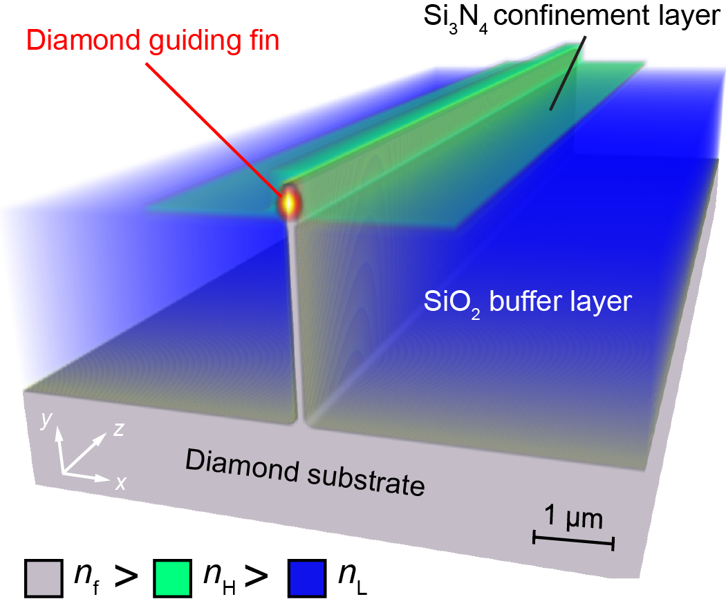
Here, we propose a new type of waveguide optimized for high-index substrates that utilizes stacked dielectric layers to confine light in the top of a fin of high-index material. An example of a SiO2/Si3N4 stack on a diamond fin/substrate at a wavelength of is shown in Fig. 1. Although the refractive index of both the buffer and confinement layers ( and , respectively) are lower than that of the fin and substrate (), the proposed design achieves confinement by engineering the effective index, resulting in an optical mode confined within the high-index material (diamond in the case of Fig. 1). This waveguide mode can propagate without leaking power into the underlying substrate, while the waveguide itself can be fabricated using conventional top-down lithography, etching, dielectric deposition, and planarization techniques. Our proposed architecture obviates the need for a buried low-index layer, providing a pathway towards large-area, scalable PICs on native substrates.

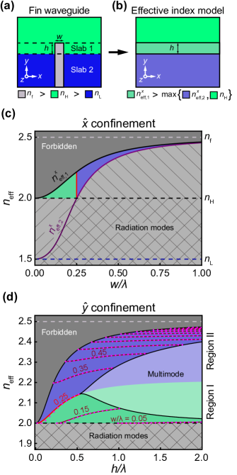
Figures 2a–b illustrate an intuitive physical picture that accounts for optical confinement in the fin waveguide geometry. By treating the two-dimensional cross-section of the -invariant waveguide dielectric topology in Fig. 2a as two stacked slab waveguides with horizontal () confinement, a slab waveguide with vertical () confinement can be formed from the slab-waveguide effective indicies in . In Fig. 2b, the two slab waveguides comprised of (Slab 1) and (Slab 2) from Fig. 2a are replaced by homogeneous layers in with the effective indices of the lowest-order supported modes and , respectively, where the effective index, , is equal to the slab waveguide propagation constant in , , of Slab divided by the free space wavenumber, . The dispersion curves of the two slabs as a function of the normalized waveguide width, , are shown in Fig. 2c with example refractive index values of , , and .
This treatment is key to understanding the nature of confinement in the fin structure: a fin mode exists when the effective index of the two-dimensionally confined structure, , satisfies the condition: , as indicated by the green and blue shaded regions in Fig. 2c. When this condition is not met, the confined modes are degenerate with a continuum of radiation modes and become leaky, as indicated by the gray hatched region in Fig. 2c. As a consequence of the effective index confinement in the fin structure, only a single-mode in is supported for the refractive index values chosen in Fig. 2c. Higher-order modes can be confined for a different choice of material indices, but only if higher-order modes of Slab 1 are contained in the blue or green shaded region of Fig. 2c, i.e., they have an effective index larger than the lowest-order mode of Slab 2.
The supported modes of the two-dimensionally-confined structure are found by solving for the modes of the -confined slab waveguide in Fig. 2b. The resulting fin mode dispersion as a function of normalized waveguide height, , (Fig. 2d) has two distinct regions that depend on the fin width, :
- Region I
-
; (green shading),
- Region II
-
; (blue shading).
The boundary between these two regions occurs when at a width that we label , which is indicated by a vertical red line in Fig. 2c and the red dispersion curve () in Fig. 2d. For an asymmetric slab waveguide, the higher-refractive-index cladding determines both the cut-off condition and the effective mode width. In Region I, the properties of the asymmetric waveguide are determined by , while in Region II, this role is taken by . The change in cut-off condition between the two regions causes the inflection point in the the cut-off height (boundary for the multimode region in Fig. 2d) at . While the fin waveguide can only be single or few mode in width, it can be multimode in height, as indicated in Fig. 2d.

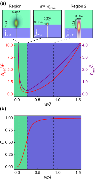
The dispersion curves provide the allowable geometry and wavelength at which confined modes are supported. Within these constraints, the mode area, , and confinement factor, , which quantifies the overlap between the optical mode and the guiding material, provide useful design metrics for maximizing light-matter interactions in fin waveguides (see Supplementary Section 1 for definitions of these parameters). In Fig 3a, we calculate for a series of , and plot the minimum, , along with the corresponding height, . Mode intensity profiles for three values of are also shown in Fig. 3a, and the corresponding at is plotted in Fig. 3b.
In Region I most of the field penetration occurs in the confinement layer, relaxing the requirements on the buffer layer thickness for low leakage at the expense of reduced . Conversely, in Region II increases with , approaches unity, and the mode extends within the fin into the buffer layer. Waveguides designed in this region may be desirable for high-power applications. The tightest confinement (smallest ) occurs at , which also corresponds to the maximum group index, , where is the vacuum speed of light and is the modal group velocity (see Supplementary Section 1), making an ideal design criterion for applications in non-linear or quantum optics. The waveguide properties in Figs. 2 and 3 have been calculated for the lowest-order mode with the dominant electric field component along . Discussion of higher order modes and further details of our semi-analytical and numerical calculations are provided in Supplementary Section 1.
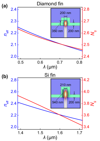
To illustrate the potential of the fin waveguide, we explore geometries in two important material platforms for PICs: diamond and silicon. The diamond waveguide is designed with an SiO2 buffer layer, a conformal -thick Si3N4 confinement layer, and SiO2 overcladding for single-mode operation at . The operating wavelength corresponds to the nitrogen-vacancy center zero phonon line Faraon_NP_11 , which is used to achieve coherent spin-light interactions Buckley_Science_10 and distributed entanglement Bernien_Nature_13 between diamond spins. We design the waveguide for the tightest confinement with as discussed above. The waveguide dispersion curve and group index is shown in Fig. 4a, along with the waveguide dimensions and calculated mode intensity profile at in the inset. We calculate that for a buffer layer thickness exceeding the propagation loss due to substrate leakage is , which is small enough that scattering due to fabrication imperfections in a realistic device would be expected to dominate. The bending loss for a bend radius of is determined to be per bend with a buffer layer thickness of , corresponding to an unloaded exceeding 30,000 for a 20 -diameter ring resonator.
Similarly, the silicon waveguide depicted in the inset to Fig. 4b is designed for minimum mode area at for telecommunications applications. With a buffer layer thickness exceeding , the propagation loss due to substrate leakage is calculated to be . The bending loss for a bend radius of is determined to be per bend with a buffer layer of , corresponding to an unloaded exceeding 10,000 for a ring resonator. Additional details regarding the design and modeling of fin waveguides are provided in Supplementary Section 2.

The design strategy described in this paper provides a straightforward pathway towards the implementation of a full PIC architecture based on monolithic fin waveguides. The required aspect ratios of the fins in Fig. 4 can be achieved through dry etching Wu_JAP_10 ; Hausmann_DRM_10 , and the dielectric stack can be fabricated using standard deposition, planarization, and lithography techniques. Although the examples in Fig. 4 use a SiO2/Si3N4 dielectric stack, the fin waveguide can be designed for any pair of materials with . Potential alternatives for the confinement layer include Al3O2 (), AlN (), SU-8 (), and Hydex ( to 1.9) Moss_NP_13 , and a full stack can also be designed using polymer layers Halldorsson_OpEx_10 , or chalcogenide glasses Eggleton_NP_11 . The compatibility of this design with a number of different materials platforms allows for integration in a diverse range of fabrication processes. For example, active devices for silicon PICs could be achieved through the realization of vertical -- junctions Liu_OpEx_07 aligned with the fin waveguide. One challenge with the proposed architecture is the incorporation of devices that are typically multimode, such as Y-branches and grating couplers, since higher-order modes in are leaky. We envision a solution to this challenge in the form of supermode devices Yariv_07 , where multimode propagation is achieved by coupled arrays of single-mode waveguides.
In summary, we have proposed a new waveguide design for native high-refractive-index substrates. This method is compatible with standard fabrication processes and alleviates the need for a buried low-index layer, providing a potential route for CMOS-compatible co-integration of silicon photonics with VLSI electronics. For InP-based PICs, the fin waveguide design provides an alternative to the InGaAs guiding layer, providing much higher confinement and a smaller mode area. Furthermore, the geometry can be adapted for any high-index substrate material, which will lead to rapid development of PICs on emerging materials platforms for quantum information processing and sensing applications.
Acknowledgments
We thank F. Aflatouni, J. B. Driscoll, S. A. Mann, A. L. Exarhos, and D. A. Hopper for helpful discussions and careful reading of the manuscript. We acknowledge financial support for this research from the University of Pennsylvania.
References
- (1) G. T. Reed, ed., Silicon photonics: The State of the Art (John Wiley & Sons, Chichester, UK, 2008).
- (2) L. Coldren, S. C. Nicholes, L. Johansson, S. Ristic, R. S. Guzzon, E. J. Norberg, U. Krishnamachari et al., “High performance InP-based photonic ICs–a tutorial,” IEEE J. Lightwave Technol. 29, 554–570 (2011).
- (3) M. Smit, X. Leijtens, H. Ambrosius, E. Bente, J. van der Tol, B. Smalbrugge, T. de Vries, E.-J. Geluk, J. Bolk, R. van Veldhoven et al., “An introduction to inp-based generic integration technology,” Semicond. Sci. Technol. 29, 083001 (2014).
- (4) S. Rumley, D. Nikolova, R. Hendry, Q. Li, D. Calhoun, and K. Bergman, “Silicon photonics for exascale systems,” IEEE J. Lightwave Technol. 33, 547–562 (2015).
- (5) L. C. Kimerling, D.-L. Kwong, and K. Wada, “Scaling computation with silicon photonics,” MRS Bulletin 39, 687–695 (2014).
- (6) I. Aharonovich, A. D. Greentree, and S. Prawer, “Diamond photonics,” Nature Photon. 5, 397–405 (2011).
- (7) S. Castelletto, J. Harrison, L. Marseglia, A. Stanley-Clarke, B. Gibson, B. Fairchild, J. Hadden, Y. D. Ho, M. Hiscocks, K. Ganesan et al., “Diamond-based structures to collect and guide light,” New J. Phys. 13, 025020 (2011).
- (8) A. Faraon, P. E. Barclay, C. Santori, K.-M. C. Fu, and R. G. Beausoleil, “Resonant enhancement of the zero-phonon emission from a colour centre in a diamond cavity,” Nature Photon. 5, 301–305 (2011).
- (9) M. J. Burek, Y. Chu, M. S. Liddy, P. Patel, J. Rochman, S. Meesala, W. Hong, Q. Quan, M. D. Lukin, and M. Lončar, “High quality-factor optical nanocavities in bulk single-crystal diamond,” Nat. Comm. 5 (2014).
- (10) N. Thomas, R. J. Barbour, Y. Song, M. L. Lee, and K.-M. C. Fu, “Waveguide-integrated single-crystalline gap resonators on diamond,” Opt. Express 22, 13555–13564 (2014).
- (11) S. L. Mouradian, T. Schröder, C. B. Poitras, L. Li, J. Goldstein, E. H. Chen, J. Cardenas, M. L. Markham, D. J. Twitchen, M. Lipson, and D. Englund, “The scalable integration of long-lived quantum memories into a photonic circuit,” Phys. Rev. X 5, 031009 (2015).
- (12) B. Hausmann, I. Bulu, V. Venkataraman, P. Deotare, and M. Lončar, “Diamond nonlinear photonics,” Nature Photon. 8, 369–374 (2014).
- (13) P. Latawiec, V. Venkataraman, M. J. Burek, B. J. Hausmann, I. Bulu, and M. Lončar, “On-chip diamond raman laser,” Optica 2, 924–928 (2015).
- (14) J. Cardenas, M. Yu, Y. Okawachi, C. B. Poitras, R. K. Lau, A. Dutt, A. L. Gaeta, and M. Lipson, “Optical nonlinearities in high-confinement silicon carbide waveguides,” Opt. lett. 40, 4138–4141 (2015).
- (15) W. Gao, A. Imamoglu, H. Bernien, and R. Hanson, “Coherent manipulation, measurement and entanglement of individual solid-state spins using optical fields,” Nature Photon. 9, 363–373 (2015).
- (16) J. Weber, W. Koehl, J. Varley, A. Janotti, B. Buckley, C. Van de Walle, and D. D. Awschalom, “Quantum computing with defects,” Proc. Natl. Acad. Sci. U. S. A. 107, 8513–8518 (2010).
- (17) D. D. Awschalom, L. C. Bassett, A. S. Dzurak, E. L. Hu, and J. R. Petta, “Quantum spintronics: engineering and manipulating atom-like spins in semiconductors,” Science 339, 1174–1179 (2013).
- (18) C. Sun, M. Georgas, J. Orcutt, B. Moss, Y.-H. Chen, J. Shainline, M. Wade, K. Mehta, K. Nammari, E. Timurdogan et al., “A monolithically-integrated chip-to-chip optical link in bulk CMOS,” IEEE J. Solid-State Circuits 50, 828–844 (2015).
- (19) J. S. Orcutt, A. Khilo, C. W. Holzwarth, M. A. Popović, H. Li, J. Sun, T. Bonifield, R. Hollingsworth, F. X. Kärtner, H. I. Smith et al., “Nanophotonic integration in state-of-the-art CMOS foundries,” Opt. Express 19, 2335–2346 (2011).
- (20) P. T. Lin, V. Singh, Y. Cai, L. C. Kimerling, and A. Agarwal, “Air-clad silicon pedestal structures for broadband mid-infrared microphotonics,” Opt. Lett. 38, 1031–1033 (2013).
- (21) B. B. Buckley, G. D. Fuchs, L. C. Bassett, and D. D. Awschalom, “Spin-light coherence for single-spin measurement and control in diamond,” Science 330, 1212–1215 (2010).
- (22) H. Bernien, B. Hensen, W. Pfaff, G. Koolstra, M. Blok, L. Robledo, T. Taminiau, M. Markham, D. Twitchen, L. Childress et al., “Heralded entanglement between solid-state qubits separated by three metres,” Nature 497, 86–90 (2013).
- (23) B. Wu, A. Kumar, and S. Pamarthy, “High aspect ratio silicon etch: a review,” J. Appl. Phys. 108, 051101 (2010).
- (24) B. J. Hausmann, M. Khan, Y. Zhang, T. M. Babinec, K. Martinick, M. McCutcheon, P. R. Hemmer, and M. Lončar, “Fabrication of diamond nanowires for quantum information processing applications,” Diamond and Related Materials 19, 621–629 (2010).
- (25) D. J. Moss, R. Morandotti, A. L. Gaeta, and M. Lipson, “New cmos-compatible platforms based on silicon nitride and hydex for nonlinear optics,” Nature Photon. 7, 597–607 (2013).
- (26) J. Halldorsson, N. B. Arnfinnsdottir, A. B. Jonsdottir, B. Agnarsson, and K. Leosson, “High index contrast polymer waveguide platform for integrated biophotonics,” Opt. express 18, 16217–16226 (2010).
- (27) B. J. Eggleton, B. Luther-Davies, and K. Richardson, “Chalcogenide photonics,” Nature Photon. 5, 141–148 (2011).
- (28) A. Liu, L. Liao, D. Rubin, H. Nguyen, B. Ciftcioglu, Y. Chetrit, N. Izhaky, and M. Paniccia, “High-speed optical modulation based on carrier depletion in a silicon waveguide,” Opt. Express 15, 660–668 (2007).
- (29) A. Yariv and P. Yeh, Photonics: optical electronics in modern communications (Oxford Univ. Press, New York, 2007), 6th ed.