Fano Resonance in an Electrically Driven Plasmonic Device
Abstract
We present an electrically driven plasmonic device consisting of a gold nanoparticle trapped in a gap between two electrodes. The tunneling current in the device generates plasmons, which decay radiatively. The emitted spectrum extends up to an energy that depends on the applied voltage. Characterization of the electrical conductance at low temperatures allows us to extract the voltage drop on each tunnel barrier and the corresponding emitted spectrum. In several devices we find a pronounced sharp asymmetrical dip in the spectrum, which we identify as a Fano resonance. Finite-difference time-domain (FDTD) calculations reveal that this resonance is due to interference between the nanoparticle and electrodes dipolar fields, and can be conveniently controlled by the structural parameters.
Keywords: Electrically driven plasmon; Plasmonics; Single Electron Transistor; Metallic nanoparticles; Fano Resonance; Photonic devices;
Contributed equally to this work \altaffiliationContributed equally to this work
Electrically driven plasmonic devices may offer unique opportunities as a research tool and for practical applications1, 2, 3, 4, 5. In such devices, current that flows across a metallic tunnel junction excites a plasmon, which gives rise to light emission. The generation of the plasmon at the tunnel junction6 is equivalent to feeding an antenna at its source. In that sense, it is different from regular optical excitation of plasmons, where the far field illumination is coupled to the plasmonic antenna, and then coupled out. This local nature of the excitation allows easy access into evanescent (or ”dark”) modes, which are not easily excited by far field illumination7, 6. From a more practical point of view, such devices may pave the way for easy realization of on-chip optical communication and sensors8, 9, 10, 5, 11, 12.
The possibility to generate light in tunnel junctions was first suggested and demonstrated more than four decades ago. Light emission in metal-oxide-metal planar tunnel junctions was observed and was attributed to plasmon mediated tunneling13, 14, 15, 16. A renewed interest in this phenomenon occurred in the early nineties, when light emission was reported in STM experiments17, 18, 19. The excellent control over the tunneling barrier in this system allowed detailed investigation of the light emission process. Recently, this concept was implemented in planar plasmonic structure, consisting of a metallic nanoparticle between two larger electrodes20.
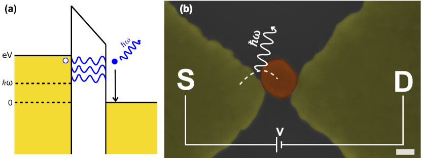
The mechanism of light emission in such structures is well understood. Consider a metallic tunnel junction, biased by a voltage , as depicted in Figure 1(a). During the tunneling process electrons may lose a fraction or all of their initial energy , exciting a plasmon, and consequently emitting photons. One may express the emitted power as
| (1) |
where is the plasmonic spectrum, and is the power spectrum of the generator current, which can be expressed as , where represents the tunneling matrix element operator. It is evident that at the limit of energy independent tunneling and zero temperature one can approximate this expression by15, 16, 21, 22
| (2) |
where is the DC junction resistance, and the applied voltage determines the maximal emitted photon energy. In practice, the tunneling rate does depend on energy, and the linear dependence on voltage is a good approximation only for . Furthermore, it was shown that photon emission at energies larger than can also be obtained. This is attributed to high order processes, in which an electron relaxation is accompanied by an excitation of another electron to an energy above the Fermi level23, 24, 25.

In this paper we use a single electron transistor (SET) as a light emitting device. The general structure of the device is shown in Figure 1(b): electrons tunnel from the source electrode (S) to the nanoparticle (NP) and then into the drain electrode (D). We show that the use of this structure allows us to properly characterize the electrical properties of the two tunnel barriers, and determine their role in the light emission process. In some devices we find a Fano resonance, resulting from interference between the nanoparticle and electrodes dipolar fields. This resonance is seen due to the local nature of the excitation, and is manifested as a sharp asymmetrical spectral dip. We show that the spectral position of this resonance can be conveniently controlled by the design of the structural parameters.
We have previously demonstrated a technique of preparing metallic NP-based SET devices26, 27. A bow-tie electrode structure is patterned by e-beam lithography on n-doped silicon substrate covered by a SiO2 layer. Gold NPs of diameter are chemically synthesized28 and covered by a dense capping layer of mercaptosuccinic acid. The thickness of this layer is , defining a sub-nanometer tunnel barrier between the NP and the electrodes. The NPs are brought into a gap of between the two electrodes by means of electrostatic trapping\bibnotemark[2]. This provides an easy process, by which several devices can be simultaneously prepared. Optical and electrical measurements were conducted in vacuum inside an optical cryostat (Janis Research ST-500HT), both at room temperature and at cryogenic temperatures ().
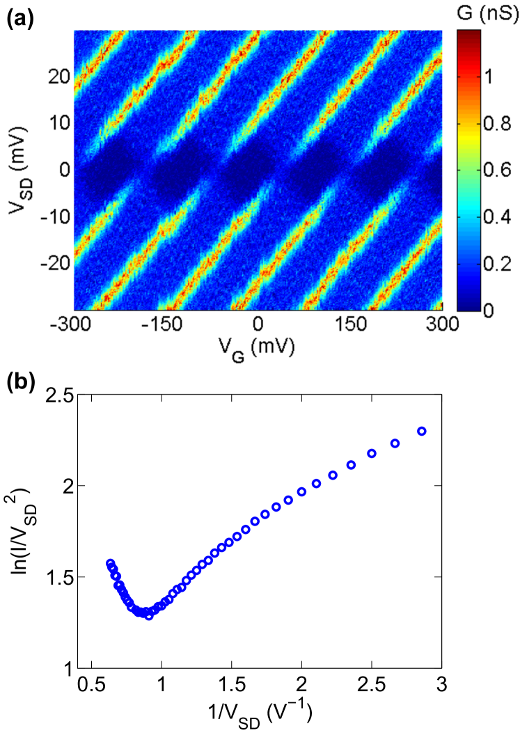
Figure 2(a) shows the measured differential conductance of a typical device at the plane, where and are the source-drain and gate voltages, respectively. The characteristic diamonds structure consisting of low conductance Coulomb blockade regions is clearly seen near . As we move along the axis, each diamond corresponds to charging the NP by an additional electron. It is evident that this structure is highly asymmetric: strong conductance peaks appear at the upper left and lower right boundaries of the diamonds, and they are much weaker at the opposite sides. This asymmetry becomes more visible at higher voltages, where it is seen as parallel conductance lines. The origin of this asymmetry is the difference in tunnel conductance between the two barriers. By fitting the measurement to a conductance model26, 27 we could extract the relevant parameters characterizing each barrier\bibnotemark[2], and in particular the tunnel conductance and of the two barriers. We note that the ratio between these two conductances determines the division of between the two barriers. In this particular device we obtain that and , implying that more than of the voltage falls on barrier . We shall later see the implications of this asymmetry on the emission spectrum in these devices, as compared to symmetric devices.
Light emission in the visible range occurs for , much larger than the charging energy of our devices (). In this regime multiple transmission channels are possible and the device functions as a simple tunnel junction. The current-voltage relation at this regime is shown in Figure 2(b), where we use the Fowler-Nordheim representation. One can see that at the curve follows the Fowler-Nordheim equation, , which describes tunneling through a trapezoidal barrier ( reflects the barrier parameters). While the high voltage limit is far beyond the Coulomb blockade regime, the characteristic conductances values, and , measured at the low voltage still characterize the voltage division between the two barriers.

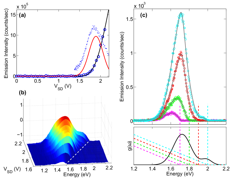
Optical measurements were performed using a Nikon Eclipse Ti-E optical microscope with a X objective (NA=), equipped with an Andor Shamrock i Imaging Spectrograph and a Andor iXon EMCCD camera. We find that as increases above a bright spot appears at the center of the bow-tie structure, and becomes brighter as the voltage is further increased. This behavior is summarized in Figure 3(a), where the total number of counts is plotted as a function of the applied voltage .
The observed rise of at is due to two factors: (i) Enhanced tunneling rate, which is linear in , as given by the current power spectrum in eq. (2). (ii) Plasmonic enhancement - moving the cutoff voltage across the plasmonic spectrum, .
It is interesting to note that this measurement of can directly provide the plasmonic spectrum. It can be easily shown13 that , hence, by simply measuring the total emitted light intensity as a function of voltage one can obtain the plasmonic spectrum of such a structure. Figure 3(a) demonstrates the strength of this technique by comparing the spectrum obtained through this procedure to an independent measurement of the light scattering spectrum (in order to minimize the numerical noise we first performed a fit to the curve and then took its numerical derivative). By performing this procedure on different structures, with different plasmonic resonances, we have verified that this procedure indeed yields the correct spectrum\bibnotemark[2]. Clearly, to obtain fine features in the spectrum one needs to conduct measurements with high signal-to-noise ratio.

Let us now turn to study the evolution of the emitted spectrum with voltage. As the voltage increases, the emitted spectrum evolves due to an increased tunneling rate and a larger overlap of the excitation energies with the plasmonic spectrum. Figure 3(b) shows a compilation of spectra, at intervals between and , measured by dispersing the emitted light into a spectrometer (the intensity is presented on a logarithmic scale). Indeed, one can clearly observe how the high energy part of the plasmonic spectrum builds up with increasing voltage and the overall intensity becomes higher. The cutoff energy exactly at can be clearly seen in the figure. We find that we could use eq. (2) to fit all the spectra, using the same plasmonic spectrum, , and linear excitation power spectrum, . This is demonstrated for four spectra in Figure 3(c).
An implicit assumption that we used in the fits of Figure 3(c) was that , namely - all the voltage that is applied on the device falls on one barrier. As was shown in Figure 2(a) this is indeed the case for very asymmetric devices, where , but is not generally true. Measurements of different, more symmetric devices, where , show a cutoff energy which is significantly lower than , up to a factor of two\bibnotemark[2]. We find that such symmetric devices experience large temporal fluctuations in the spectral lineshape, and in particular in the cutoff energy. In these devices small changes in the tunnel junction conductances may result in a significant different voltage division, and consequently - different cutoff energy. This emphasizes the importance of the low voltage characterization at low temperatures.
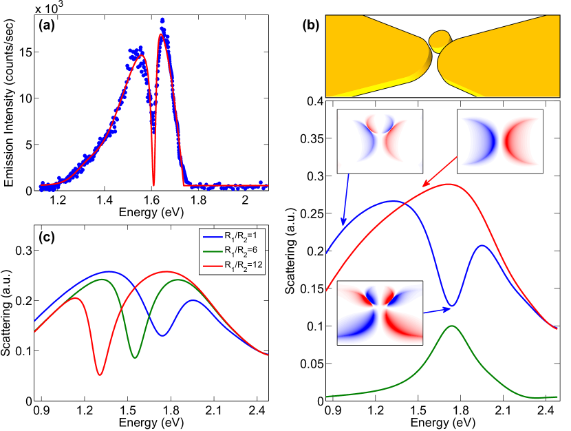
An important feature of electrically driven plasmon is the local nature of the excitation. Contrary to a scattering measurement, in which plasmons are excited over a macroscopic area, here the plasmons are generated at the tunnel barrier over which the voltage drops. In that sense, this method is similar to electron energy loss spectroscopy (EELS), where a focused beam of electron excites a plasmon locally30. The implication is that we are able to probe local features of the plasmonic spectrum . This is well manifested in our bow-tie structure: while the far field scattering spectrum is dominated by contributions of the large size electrodes, the local excitation emphasizes fine features arising from plasmonic interactions in the gap region. Indeed, in several devices ( out of the measured) we find a peculiar spectrum, characterized by two adjacent peaks, with an asymmetric dip between them, as shown in Figure 4(a). We obtain a good fit of this spectrum to a Fano behavior , with a Fano factor , indicating a strong interference between two resonances.

To explain the appearance of a Fano resonance31, 32 in our structure we use a simple toy-model, consisting of infinite electrodes and a metal NP disk between them (top of Figure 4(b)). We calculate the plasmonic spectrum of this structure using Finite-difference time-domain (FDTD) method\bibnotemark[2]. Figure 4(b) shows the calculated scattering spectrum obtained by exciting a small region around the disk. This excitation scheme is a simple way to represent the local nature of the excitation in our experiments. Remarkably, one obtains in this simple toy-model the clear Fano hallmarks: strong asymmetry and a pronounced interference dip between the peaks. As seen, these features appear only when the disk is present. We have verified that similar spectra are obtained when the disk is replaced by a sphere. Our calculations clearly demonstrate the importance of the local nature of the excitation in the observation of the Fano resonance. We find that when we expand the illumination area the Fano feature gradually disappears, and a simple single broad peak remains. It is seen that the experimental spectral features (scattering and emission, Figures 3,4(a)) are narrower than those obtained in the simulation. This difference is explained in detail in the Supporting Information.
To understand how the Fano spectrum is created here it is instructive to examine the spatial charge distribution at the surface (represented by the normal electric field component), as shown in Figure 4(b). It is seen that without the NP we obtain a simple dipolar distribution around the gap. This is manifested as a broad spectral lineshape, which serves as the continuum in the Fano representation33. The introduction of the NP radically changes this charge distribution: the induced dipolar field at the NP forces an overall quadrupole-like distribution in the structure, which suppresses the far field emission7, 34.
In order to demonstrate that the dip is indeed due to destructive interference between the NP and the electrodes resonances, we ”turn off” this interference by exciting the structure with a dipole, localized at the NP center. This way of excitation affects mainly the NP, and the electrodes are only weakly excited. The calculated spectrum under this excitation condition shows a clear peak, which is located at exactly the same spectral position as the Fano dip (Figure 4(b)). This proves that indeed the electrodes play the role of a continuum, and the NP - of the narrow resonance.
The particle in a bow-tie structure allows easy control of the Fano resonance. This is demonstrated in Figure 4(c), where the eccentricity of the NP is gradually changed, from a circular disk to a narrow ellipse, while keeping the other structural parameters fixed. Remarkably, the Fano dip moves to lower energy and becomes narrower, following the corresponding changes in the NP resonance spectral position and width. On the other hand, the Fano resonance is relatively insensitive to the details of the electrodes design: when changing the angle of the bow-tie electrodes we find that the Fano dip remains at approximately the same spectral position\bibnotemark[2]. It is important to note, however, that as the NP is moved down towards the bow-tie center, the Fano resonance disappears7. This could explain the fact that the resonance is observed only in some of the devices: we believe that in these devices the NP was trapped off the bow-tie center.
Fano resonances in plasmonic structures are of great recent interest7, 35, 36, 37, 38, 39, 32, 40, 33, 34. It is suggested that their sharp characteristic spectral features and sensitivity to the sample parameters may turn them into efficient sensors. In that sense, the ability to generate such resonances in electrically driven devices may amplify their potential. Furthermore, the separate control of the interfering broad and narrow modes in these devices offers an easy way of engineering the Fano resonance. Such devices may be a step toward the realization of an on-chip, controllable nano-optical emitters and sensors, and be of a great interest to the near-field microscopy community.
Nanoparticle synthesis and device fabrication methods; Single dot simulation; Symmetrical and asymmetrical conductance devices; FDTD simulation details; Fano resonance measurements;
The authors declare no competing financial interest.
We would like to thank D. Mahalu and O. Raslin for their help in the electron beam lithography.
[2]See Supporting Information
References
- García de Abajo 2010 García de Abajo, F. J. Rev. Mod. Phys. 2010, 82, 209–275
- Fan et al. 2012 Fan, P.; Colombo, C.; Huang, K. C. Y.; Krogstrup, P.; Nygård, J.; Fontcuberta i Morral, A.; Brongersma, M. L. Nano Lett. 2012, 12, 4943–4947
- Li and Stockman 2013 Li, D.; Stockman, M. I. Phys. Rev. Lett. 2013, 110, 106803
- Rai et al. 2013 Rai, P.; Hartmann, N.; Berthelot, J.; Arocas, J.; Colas des Francs, G.; Hartschuh, A.; Bouhelier, A. Phys. Rev. Lett. 2013, 111, 026804
- Sheldon et al. 2014 Sheldon, M. T.; van de Groep, J.; Brown, A. M.; Polman, A.; Atwater, H. A. Science 2014, 346, 828–831
- Savage et al. 2012 Savage, K. J.; Hawkeye, M. M.; Esteban, R.; Borisov, A. G.; Aizpurua, J.; Baumberg, J. J. Nature 2012, 491, 574–577
- Hao et al. 2008 Hao, F.; Sonnefraud, Y.; Van Dorpe, P.; Maier, S. a.; Halas, N. J.; Nordlander, P. Nano Lett. 2008, 8, 3983–3988
- Bendaña et al. 2011 Bendaña, X.; Polman, A.; García de Abajo, F. J. Nano Lett. 2011, 11, 5099–5103
- Jeong et al. 2013 Jeong, K.-Y.; No, Y.-S.; Hwang, Y.; Kim, K. S.; Seo, M.-K.; Park, H.-G.; Lee, Y.-H. Nat. Commun. 2013, 4, 1–6
- Huang et al. 2014 Huang, K. C. Y.; Seo, M.-K.; Sarmiento, T.; Huo, Y.; Harris, J. S.; Brongersma, M. L. Nat. Photonics 2014, 8, 244–249
- Cox and Javier García de Abajo 2014 Cox, J. D.; Javier García de Abajo, F. Nat. Commun. 2014, 5, 5725
- Tielrooij et al. 2015 Tielrooij, K. J.; Orona, L.; Ferrier, A.; Badioli, M.; Navickaite, G.; Coop, S.; Nanot, S.; Kalinic, B.; Cesca, T.; Gaudreau, L. et al. Nat. Phys. 2015, 11, 281–287
- Lambe and McCarthy 1976 Lambe, J.; McCarthy, S. L. Phys. Rev. Lett. 1976, 37, 923–925
- Hansma and Broida 1978 Hansma, P. K.; Broida, H. P. Appl. Phys. Lett. 1978, 32, 545
- Hone et al. 1978 Hone, D.; Muhlschlegel, B.; Scalapino, D. J. Appl. Phys. Lett. 1978, 33, 203
- Rendell and Scalapino 1981 Rendell, R. W.; Scalapino, D. J. Phys. Rev. B 1981, 24, 3276–3294
- Coombs et al. 1988 Coombs, J. H.; Gimzewski, J. K.; Reihl, B.; Sass, J. K.; Schlittler, R. R. J. Microsc. (Oxford, U. K.) 1988, 152, 325–336
- Gimzewski et al. 1989 Gimzewski, J. K.; Sass, J. K.; Schlitter, R. R.; Schott, J. Europhys. Lett. 1989, 8, 435–440
- Berndt et al. 1991 Berndt, R.; Gimzewski, J. K.; Johansson, P. Phys. Rev. Lett. 1991, 67, 3796–3799
- Kern et al. 2015 Kern, J.; Kullock, R.; Prangsma, J.; Emmerling, M.; Kamp, M.; Hecht, B. Nat. Photonics 2015, 9, 582–586
- Persson and Baratoff 1992 Persson, B. N. J.; Baratoff, A. Phys. Rev. Lett. 1992, 68, 3224–3227
- Uehara et al. 1992 Uehara, Y.; Kimura, Y.; Ushioda, S.; Takeuchi, K. Jpn. J. Appl. Phys. 1992, 31, 2465–2469
- Schneider et al. 2013 Schneider, N. L.; Johansson, P.; Berndt, R. Phys. Rev. B 2013, 87, 045409
- Kaasbjerg and Nitzan 2015 Kaasbjerg, K.; Nitzan, A. Phys. Rev. Lett. 2015, 114, 1–6
- Buret et al. 2015 Buret, M.; Uskov, A. V.; Dellinger, J.; Cazier, N.; Mennemanteuil, M.-M.; Berthelot, J.; Smetanin, I. V.; Protsenko, I. E.; Colas-des Francs, G.; Bouhelier, A. Nano Lett. 2015, 15, 5811–5818
- Guttman et al. 2011 Guttman, A.; Mahalu, D.; Sperling, J.; Cohen-Hoshen, E.; Bar-Joseph, I. Appl. Phys. Lett. 2011, 99, 063113
- Vardi et al. 2014 Vardi, Y.; Guttman, A.; Bar-Joseph, I. Nano Lett. 2014, 14, 2794–2799
- Cohen-Hoshen et al. 2012 Cohen-Hoshen, E.; Bryant, G. W.; Pinkas, I.; Sperling, J.; Bar-Joseph, I. Nano Lett. 2012, 12, 4260–4
- 29 See Supporting Information
- Coenen et al. 2015 Coenen, T.; Schoen, D. T.; Mann, S. A.; Rodriguez, S. R. K.; Brenny, B. J. M.; Polman, A.; Brongersma, M. L. Nano Lett. 2015, 151016141704002
- Fano 1961 Fano, U. Phys. Rev. 1961, 124, 1866–1878
- Miroshnichenko et al. 2010 Miroshnichenko, A. E.; Flach, S.; Kivshar, Y. S. Rev. Mod. Phys. 2010, 82, 2257–2298
- Giannini et al. 2011 Giannini, V.; Francescato, Y.; Amrania, H.; Phillips, C. C.; Maier, S. A. Nano Lett. 2011, 11, 2835–2840
- Wu et al. 2011 Wu, C.; Khanikaev, A. B.; Adato, R.; Arju, N.; Yanik, A. A.; Altug, H.; Shvets, G. Nat. Mater. 2011, 11, 69–75
- Neubrech et al. 2008 Neubrech, F.; Pucci, A.; Cornelius, T. W.; Karim, S.; García-Etxarri, A.; Aizpurua, J. Phys. Rev. Lett. 2008, 101, 157403
- Aizpurua et al. 2008 Aizpurua, J.; Taubner, T.; García de Abajo, F. J.; Brehm, M.; Hillenbrand, R. Opt. Express 2008, 16, 1529
- Verellen et al. 2009 Verellen, N.; Sonnefraud, Y.; Sobhani, H.; Hao, F.; Moshchalkov, V. V.; Dorpe, P. V.; Nordlander, P.; Maier, S. A. Nano Lett. 2009, 9, 1663–1667
- Fan et al. 2010 Fan, J. a.; Wu, C.; Bao, K.; Bao, J.; Bardhan, R.; Halas, N. J.; Manoharan, V. N.; Nordlander, P.; Shvets, G.; Capasso, F. Science 2010, 328, 1135–1138
- Luk’yanchuk et al. 2010 Luk’yanchuk, B.; Zheludev, N. I.; Maier, S. A.; Halas, N. J.; Nordlander, P.; Giessen, H.; Chong, C. T. Nat. Mater. 2010, 9, 707–715
- Pryce et al. 2010 Pryce, I. M.; Aydin, K.; Kelaita, Y. A.; Briggs, R. M.; Atwater, H. A. Nano Lett. 2010, 10, 4222–4227